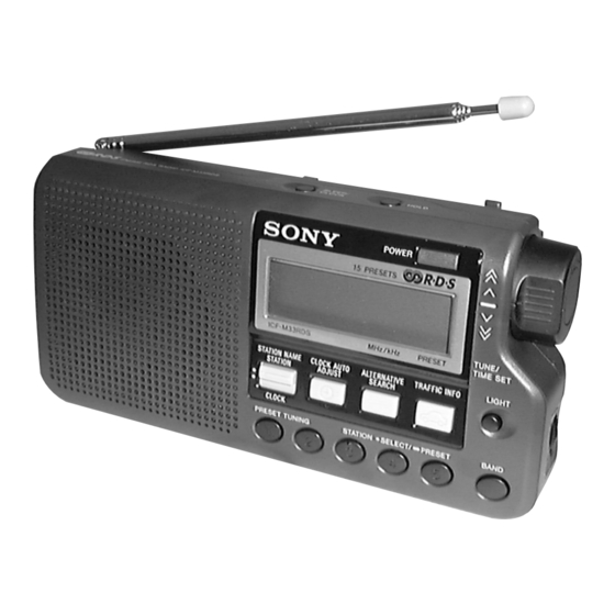
Sony ICF-M33RDS Service Manual
Fm/am (lw) rds radio
Hide thumbs
Also See for ICF-M33RDS:
- Operating instructions (2 pages) ,
- Operating instructions (2 pages) ,
- Operating instructions (2 pages)

Subscribe to Our Youtube Channel
Related Manuals for Sony ICF-M33RDS


Summary of Contents for Sony ICF-M33RDS
- Page 1 ICF-M33RDS SERVICE MANUAL AEP Model UK Model Ver 1.2 2001.02 With SUPPLEMENT-1 (9-926-922-81) SPECIFICATIONS FM/AM (LW) RDS RADIO MICROFILM...
-
Page 2: Table Of Contents
TABLE OF CONTENTS SERVICING NOTES GENERAL HOW TO CHANGED THE CERAMIC FILTERS Features ................3 This model is used two ceramic filters of CF2 and CF3. Choosing the Power Source ..........4 You must used same type of color marked ceramic filters in order Setting the Clock ............. - Page 3 SECTION 1 This section is extracted from instruction manual. GENERAL – 3 –...
- Page 4 – 4 –...
- Page 5 – 5 –...
- Page 6 – 6 –...
-
Page 7: Disassembly
SECTION 2 DISASSEMBLY • This set can be disassembled in the order shown below. Cabinet (Rear) Chassis Key Board Main Board Note: Follow the disassembly procedure in the numerical order given. CABINET (REAR) 2 telescopic (FM) antenna 7 hand strap 1 screw 6 ANT contact plate (nylock B3 ×... - Page 8 KEY BOARD 2 Remove the lock of 2 two flat wires two connectors (CN1, CN2). 1 three claws 3 KEY board MAIN BOARD 2 MAIN board 1 three claws – 8 –...
-
Page 9: Electrical Adjustments
SECTION 3 ELECTRICAL ADJUSTMENTS FM VCO VOLTAGE ADJUSTMENT 0 dB = 1µV [FM] Adjustment Part Frequency Display Reading On Digital voltmeter Setting: 87.5 MHz 2.5 V ± 0.1 V Band switch: FM confirmation 108.0 MHz Less than 10.7 V FM RF signal generator FM antenna in level meter... - Page 10 Adjustment Location: L2 AM (LW) Tracking Adjustment * Mounted on chassis L4 FM VCO Voltage Adjustment FM Tracking Adjustment – MAIN BOARD (Component Side) – ANTENNA IN T1 AM IF Adjustment L5 AM (LW) VCO Voltage Adjustment CT1 AM (LW) Tracking Adjustment –...
-
Page 11: Diagrams
ICF-M33RDS SECTION 4 DIAGRAMS 4-1. BLOCK DIAGRAM 4-2. NOTE FOR PRINTED WIRING BOARDS AND SCHEMATIC DIAGRAMS CT2, L3 Note on Printed Wiring Board: Note on Schematic Diagram: FM TRACKING • X : parts extracted from the component side. • All capacitors are in µF unless otherwise noted. pF: µµF FM RF •... -
Page 14: Schematic Diagrams
Ver 1.1 2000. 01 ICF-M33RDS 4-5. SCHEMATIC DIAGRAM • See page 25 for Waveforms. • See page 26 for IC Block Diagrams. (French) (French) – 21 – – 22 – – 23 – – 24 –... - Page 15 • Waveforms – KEY Board – – MAIN Board – 5 IC101 %∞ (XT1) 1 IC2 1 (X IN) 400 mV/DIV, 5 µs/DIV 500 mV/DIV, 20 µs/DIV 1 Vp-p 1.7 Vp-p 30.5 µ s 13.3 µ s 2 Q4 (COLLECTOR) 6 IC101 %ª...
- Page 16 • IC Block Diagrams – MAIN Board – IC1 CXA1019M-T6 FM FE DISCRIMINATOR FM IF AM FE AF POWER AMP TUNING METER AM IF DET AGC IC2 TC9418FN-EL 15 14 13 4 BIT 1/15, SWALLOW 1/16 COUNTER STATE STATE BUFFER BUFFER 13 BIT PHASE...
- Page 17 IC3 BU1924F 12 11 10 CLOCK TEST PLL 57kHz RDS/ARI 1187.5Hz COMPARATOR 8th SWITCHED BIPHASE CAPACITOR DECODER FILTER DEFFERENTIAL ANTI-ALIASING DECODER FILTER – 27 –...
-
Page 18: 4-6. Ic Pin Function Description
Ver 1.1 2000. 01 4-6. IC PIN FUNCTION DESCRIPTION • KEY BOARD IC101 µPD753012AGC-F05-3B9 (SYSTEM CONTROLLER, LCD DRIVER, KEY CONTROL) Pin No. Pin Name Description 1 to 20 LCD12 to LCD31 Segment drive signal output to the liquid crystal display (LCD101) 21 to 24 COM0 to COM3 Common drive signal output to the liquid crystal display (LCD101) BIAS... -
Page 19: Exploded View
SECTION 5 EXPLODED VIEW NOTE: • -XX and -X mean standardized parts, so they • Items marked “*” are not stocked since they may have some difference from the original are seldom required for routine service. Some one. delay should be anticipated when ordering •... -
Page 20: Electrical Parts List
SECTION 6 MAIN ELECTRICAL PARTS LIST NOTE: When indicating parts by reference • Due to standardization, replacements in the • Items marked “*” are not stocked since they number, please include the board. parts list may be different from the parts speci- are seldom required for routine service. - Page 21 MAIN Ref. No. Part No. Description Remark Ref. No. Part No. Description Remark < TRIMMER > 1-415-930-11 COIL(OSC) (French) 1-141-444-11 CAP, CERAMIC TRIMMER 50PF (French) 1-406-485-11 COIL(OSC) (AEP, UK) 1-141-304-21 CAP, TRIMMER 10PF (AEP, UK) 1-414-405-11 INDUCTOR 150uH 1-141-304-21 CAP, TRIMMER 10PF 1-412-006-31 INDUCTOR CHIP 10uH <...
- Page 22 Ver 1.1 2000. 01 MAIN Ref. No. Part No. Description Remark Ref. No. Part No. Description Remark < VARIABLE RESISTOR > < COIL > 1-225-441-41 RES, VAR, CARBON 50K L101 1-414-406-11 INDUCTOR 220uH L102 1-414-406-11 INDUCTOR 220uH < TRANSFORMER > <...
- Page 23 Ref. No. Part No. Description Remark Ref. No. Part No. Description Remark X102 1-781-363-21 VIBRATOR, CERAMIC (4.33MHz) ************************************************************** ACCESSORIES & PACKING MATERIALS ******************************* 3-864-831-11 MANUAL,INSTRUCTION (ENGLISH,FRENCH,GERMAN,DUTCH) 3-864-831-21 MANUAL,INSTRUCTION (ITALIAN,SPANISH,PORTGUESE,SWEDISH) 3-864-831-31 MANUAL,INSTRUCTION (FINNISH,DANISH) – 33 –...
- Page 24 ICF-M33RDS Sony Corporation 99A0542-1 Printed in Japan © 1999. 1 9-926-922-11 Parsonal A&V Products Company Published by Quality Engineering Dept. – 34 – (Shibaura)
- Page 25 ICF-M33RDS AEP Model UK Model SERVICE MANUAL 2001.02 SUPPLEMENT-1 File this supplement with the service manual. Subject: Silver model addition (ENG-01001) • Difference parts list Page Former Ref. No. Part No. Description Remark Ref. No. Part No. Description Remark 3-027-770-01 CABINET (FRONT) (AEP, UK)
-
Page 26: Revision History
ICF-M33RDS REVISION HISTORY Clicking the version allows you to jump to the revised page. Also, clicking the version at the upper right on the revised page allows you to jump to the next revised page. Ver. Date Description of Revision 2001.02...
Need help?
Do you have a question about the ICF-M33RDS and is the answer not in the manual?
Questions and answers