Advertisement
Quick Links
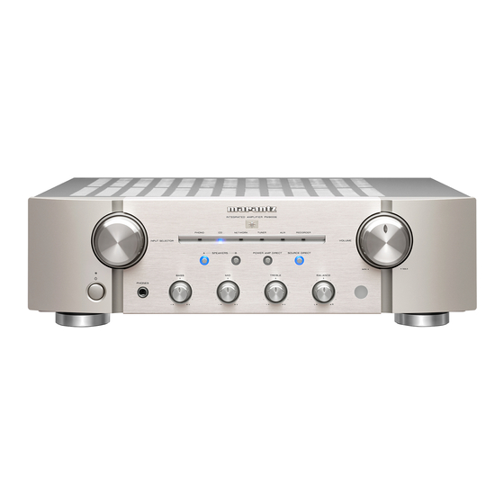
Integrated Amplifier
PM8006
• For purposes of improvement, specifications and design are subject to change without notice.
• Please use this service manual with referring to the operating instructions without fail.
• Some illustrations using in this service manual are slightly different from the actual set.
Service Manual
Click here!
On-line service parts list
http://dmedia.dmglobal.com/Document/DocumentDetails/23855
Online Parts List
(P5 to P7)
WEB owner's manual
NA:
http://manuals.marantz.com/PM8006/NA/EN/index.php (October 2017)
EU:
http://manuals.marantz.com/PM8006/EU/EN/index.php (October 2017)
AP:
http://manuals.marantz.com/PM8006/AP/ZH/index.php (November 2017)
CAUTION IN SERVICING
ELECTRICAL
MECHANICAL
REPAIR INFORMATION
UPDATING
Confidential
Ver. 1
(Release schedule)
Advertisement

Related Manuals for Marantz PM8006


Summary of Contents for Marantz PM8006
- Page 1 Integrated Amplifier Click here! PM8006 On-line service parts list http://dmedia.dmglobal.com/Document/DocumentDetails/23855 Online Parts List (P5 to P7) WEB owner’s manual (Release schedule) http://manuals.marantz.com/PM8006/NA/EN/index.php (October 2017) http://manuals.marantz.com/PM8006/EU/EN/index.php (October 2017) http://manuals.marantz.com/PM8006/AP/ZH/index.php (November 2017) CAUTION IN SERVICING ELECTRICAL MECHANICAL REPAIR INFORMATION UPDATING • For purposes of improvement, specifications and design are subject to change without notice. • Please use this service manual with referring to the operating instructions without fail.
- Page 2 CAUTION IN SERVICING SAFETY PRECAUTIONS NOTE FOR SCHEMATIC DIAGRAM NOTE FOR PARTS LIST INSTRUCTIONS FOR HANDLING SEMICONDUCTORS AND OPTICAL UNIT Online Parts List Accessing the Parts List Logging in to New SDI and Accessing the Parts List Accessing the Part List from the Model Asset Screen PRINTED CIRCUIT BOARDS Parts Table Downloading the Parts List as an Excel File Revision History...
- Page 3 SAFETY PRECAUTIONS ◎ Make a safety check after servicing! The following items should be checked for continued protection of the customer and the service Check that all screws, parts and wires removed or disconnected when servicing have been put back technician.
- Page 4 NOTE FOR SCHEMATIC DIAGRAM WARNING: Parts indicated by the z mark have critical characteristics. Use ONLY replacement parts recommended by the manufacturer. CAUTION: Before returning the set to the customer, be sure to carry out either (1) a leakage current check or (2) a line to chassis resistance check.
- Page 5 Online Parts List Accessing the Parts List Logging in to New SDI and Accessing the Parts List (1) Click the URL link on the cover of the service manual. (1) Access New SDI from the URL below. Examples of display <http://dmedia.dmglobal.com>...
- Page 6 Accessing the Part List from the Model Asset Screen Downloading the Parts List as an Excel File (1) Display Model Asset from New SDI. (1) Displays the Parts List. Click the Download icon. (2) Click the section displayed as ▼ Link to Part Lists under the model name. NOTE : If the ▼...
- Page 7 Searching Part Numbers or Ref. Numbers You can search a Parts List for part numbers or Ref. numbers. (1) Enter the part number or Ref. number in the search window of the Parts List, and press the search button. (2) The search results are displayed. The name of the sheet in which the search part is used and the part’s line are displayed.
- Page 8 CAUTION IN SERVICING. Initializing This Unit Make sure to initialize this unit after replacing the microcomputer or any peripheral equipment, or the digital PCB. 1. Press the power button to turn off the power. 2. While holding down the "SOURCE DIRECT" button, press the power button to turn on the power. 3.
- Page 9 ELECTRICAL SCHEMATIC DIAGRAMS SCH01_MAIN1 SCH02_MAIN2 and POWER STAGE SCH03_SPK TERMINAL SCH04_U-COM and SELECTOR SCH05_TONE SCH06_HEADPHONE and POWER SW and STANDBY SCH07_PHONO and VOLUME SCH08_HDAM-SA3 PRINTED CIRCUIT BOARDS MAIN, HDAM SA3, R WIRE PROTECTION, L WIRE PROTECTION, POWER STAGE SPK TERMINAL, STANDBY, POWER SW, VOLUME TONE, u-COM, PHONO AMP, HEADPHONE, STANDBY LED, INPUT SEL, CLAMP LEVEL DIAGRAM, BLOCK DIAGRAM, POWER DIAGRAM WIRING DIAGRAM...
- Page 10 SCHEMATIC DIAGRAMS SCH01_MAIN1 N3301 N2801 N2802 N2803 TO B2004 TO B2003 TO B2901 +24VL N3301 5P-EH(IM) N2801 +17V 5P-EH(IM) TO TONE PWB TO TONE PWB N2803 -17V Q3046 TO PHONO AMP PWB B2004 B2003 6P-EH(IM) B2901 KRC102S N2802 3P-EH(IM) R3031 To PHONO AMP PWB A-GND A-GND...
- Page 11 SCH02_MAIN2 and POWER STAGE Measurement condition Point A Point B Point C Point D Point E Point F Point G ・ Voltage measurement No signal ・ Waveform measurement INPUT: 500mVrms/1KHz(CD) OUTPUT: 1W at 8ohmes(2.83Vrms) +46.6 V (DC) R6065 J7007 Point D SHORT CFPS R6039...
- Page 12 SCH03_SPK TERMINAL WIRE_CLIP(01562-21) WIRE_CLIP(01562-21) 8U-110218-8 Z7513 Z7514 SPK TERMINAL PWB 65101001140AS 65101001140AS 00D2050452017 Z7501 SPK-CONTACTOR R7501 SPK_A(L) CFPS Z7502 SPK-CONTACTOR N/K VERSION ONLY Z7503 SPK-CONTACTOR SPK_B(L) Z7504 N7501 SPK-CONTACTOR N7501 4P-VH SPK_L+. Z7505 SPK_L-. SPK-CONTACTOR SPK_R-. SPK_A(R) TO POWER STAGE PWB CFPS N7009 Z7506...
- Page 13 SCH04_U-COM and SELECTOR STANDBY LED PWB R1901 N1004 12P-PH R1902 D1901 N1004 Q1252 PA_DI SLR342VC 1 PA_DI KRA102S SO_DI N1002 2 SO_DI REC_OFF TO B1201 3 RECODER N1007 3 pin WAVE FORM at STAND BY mode 8U-110219-2 B1901 4 CD_RY TO INPUT SELECTOR PWB EHR-SCN_2.5MMPICH EXP_ST...
- Page 14 SCH05_TONE D2502 D2501 D2503 D2504 D2505 D2506 5VD2 PVD09-3A2W-ELEDISHB_S2 PVD09-3A2W-ELEDISHB_S2 PVD09-3A2W-ELEDISHB_S2 PVD09-3A2W-ELEDISHB_S2 PVD09-3A2W-ELEDISHB_S2 PVD09-3A2W-ELEDISHB_S2 TUNER PHONO RECORDER PA_DI SO_DI SPK-A SPK-B N2501 12P-PH N2501 A-DI. PA_DI SO-DI. SO_DI REC_OFF. REC_OFF CD_RY EXP_ST. EXP_STROBE POWER DIRECT SOURCE DIRECT SPK-A:0V SPK-B:0V EXP_DI. PHONO:0V PHONO:0V PHONO:0V...
- Page 15 SCH06_HEADPHONE and POWER SW and STANDBY 8U-110219-6 CLAMP PWB N8503 +28V -28V TO N8101 8U-110219-7 POWER SW PWB TO MAIN PWB S8901 N8101 C8901 3P-VH D8511 R8506 N8504 470P/250V R8505 1(1W) 11EQS10 D8512 R8507 0.68UF/4.7ohm J0001 1(1W) 11EQS10 D8509 A-GND D8513 D8515 D8518...
- Page 16 SCH07_PHONO and VOLUME V4101 PHONO PWB R4073 OPEN 8U-110219-9 OPEN Q4023 2SC3324 R4075 SHORT D4009 Q4005 Q4007 OPEN D4011 R4105 OPEN 2SA1312(B) 2.2K 3 D2 2.2/100 2.2/100 A-GND. Comp C4023 C4025 R4053 C4027 C4039 Q4001 OUT1 R4055 R4081 Q4009 2SK2145GR/BL 2.2K 2SA1312(B) 34.1k...
- Page 17 SCH08_HDAM-SA3 HDAM-SA3 PWB KIT 00MKH22AJ1030 --> 63201023500AM 8U-210235 HDAM-SA3 UNIT DN01 DN03 DN04 DN02 00MWG22AJ5000 GND LINE POWER+ LINE POWER- LINE ANALOG AUDIO R ANALOG AUDIO L...
- Page 18 PRINTED CIRCUIT BOARDS MAIN, HDAM SA3, R WIRE PROTECTION, L WIRE PROTECTION, POWER STAGE Lead-free Solder When soldering, use the Lead-free Solder (Sn-Ag-Cu). MAIN (A SIDE) MAIN (B SIDE) HDAM SA3 (A SIDE) HDAM SA3 (B SIDE) 8U-210235 C3000 C3006 C3008 C3005 C3007...
- Page 19 SPK TERMINAL, STANDBY, POWER SW, VOLUME SPK TERMINAL (ASIDE) SPK TERMINAL (B SIDE) STANDBY (A SIDE) STANDBY (B SIDE) Z7513 N8506 JV199 Z8507 JV200 K8502 JV201 C8517 H8511 H8512 JV60 F8510 JV59 Z7501 JV136 JV126 Z7503 Z7504 N8501 D8512 20.0 D8510 AC INLET JV203...
- Page 20 TONE, u-COM, PHONO AMP, HEADPHONE, STANDBY LED, INPUT SEL, CLAMP TONEN (A SIDE) TONEN (B SIDE) u-COM (A SIDE) u-COM (B SIDE) PHONO AMP (A SIDE) PHONO AMP (B SIDE) 8U-110219-1 C2601 u-COM UNIT C1031 C1030 Q1030 R2602 JV140 JV105 JV22 R1035 15.0...
- Page 21 LEVEL DIAGRAM, BLOCK DIAGRAM, POWER DIAGRAM 70W 8Ω 23.6V (27.5dB) Power Amp Direct in 1.6V (4.0dB) PRE OUT 1.6V (4.0dB) CD etc. 200mV (-14.0dB) MM 2mV (-54.0dB) PHONO BLOCK FUNCTION BLOCK TONE BLOCK MAIN AMP BLOCK VOLUME REGULATOR BLOCK U-COM BLOCK...
- Page 22 WIRING DIAGRAM N1005 8U-110219-10 T0 B1008 B5901 VOLUME PCB T0 N1006 Z5902 8U-110218-8 SPEAKER TERMINAL W0008 B4000 N3301 B6001 N7001 N7009 N7501 8U110219-9 PHONO AMP PCB 8U-110218-1 MAIN PCB N7503 B2901 N2803 B6002 N7002 8U-110218-2 POWER STAGE PCB WA01 B8001 Z8201 WIRE ASSY (B3902)
- Page 23 SEMICONDUCTORS TMP86FH47AUG Only major semiconductors are shown, general semiconductors etc. are omitted to list. The semiconductor which described a detailed drawing in a schematic diagram are omitted to list. 1.2 Pin Assignment 1. IC's TMP86FH47BUG (U1001) TMP86FH47BUG Terminal Functions Port Setting Port Name I/O Use Name...
- Page 24 NJU72322V (U3201) NJU72750A (U3904) Symbol Function Symbol Function + Power Pin DATA IC Control data input InA1 Ach Input 1 CLOCK IC control clock input InB1 Bch Input 1 InA2 Ach Input 2 InB2 Bch Input 2 OutB3 Bch Output 3 InA3 Ach Input 3 OutA3...
- Page 25 <= PROGRAM <= RANDOM <= REPEAT <= INFO <= Extended Code: AMP PM8006 must receive following codes. These codes are not included in the RC001PMND RC-5/RC-5 Ext. Name System Command Extension Power On Power Off MUTE On MUTE Off PHONO...
- Page 26 MECHANICAL DISASSEMBLY Flowchart 1. FRONT ASSY 2. HEAT SINK ASSY 3. PHONO AMP PCB 4. STANDBY PCB 5. REAR PANEL ASSY 6. MAIN PCB EXPLODED VIEW PACKING VIEW...
- Page 27 DISASSEMBLY Flowchart • Remove each part following the flow below. • Reassemble the removed parts in the reverse order. • Read "SAFETY PRECAUTIONS" before reassembling the removed parts. • If wire bundles are removed or moved during adjustment or part replacement, reshape the wires after completing the work. Failure to shape the wires correctly may cause problems such as noise. •...
- Page 28 • The photographs with no shooting direction indicated were taken from the top of the unit. (1) Remove the screws. • Photos of PM8006 N1SG are used in this manual. The viewpoint of each photograph (Shooting direction : X) [View from the top] ↓Shooting direction: B↓...
- Page 29 3. PHONO AMP PCB 5. REAR PANEL ASSY Proceeding : TOP COVER → PHONO AMP PCB Proceeding : TOP COVER → REAR PANEL ASSY (1) Remove the screws. Remove the connector. (1) Remove the screws. Cut the wire clamp, then remove the connector. N3301 N8501 N7501...
- Page 30 EXPLODED VIEW http://dmedia.dmglobal.com/Document/DocumentDetails/23855 Parts List : 0040T S6 x1 J0001 0040H x6 0015R J0003-J0006 S10 x2 S6 x2 J0007-J0010 0010H S3 x4 S1 x2 S10 x2 0035T 0110R x2 Q7014 S14 x6 K7004 Q7012 0100R x8 S5 x3 S4 x2 Q7011 S4 x2 Q7013...
- Page 31 PACKING VIEW http://dmedia.dmglobal.com/Document/DocumentDetails/23855 Parts List : 0020P UK plug 0010U (UK Only) 0060U 0050U 0020U 0050P 0080P 0030U W0001 0010A 0020A 0070U 0022P 0020P 0030A 0060P 0070P 0040P 0010P 0060P 0040P...
- Page 32 REPAIR INFORMATION TROUBLE SHOOTING 1. The power cannot be turned on (STANDBY LED is not lit(STANDBY MODE)) 2. The power cannot be turned on (STANDBY LED is lit→light flashes) 3. STANDBY LED flashes while using the unit (Protection circuit becomes activated) 4.
- Page 33 TROUBLE SHOOTING 1. The power cannot be turned on 2. The power cannot be turned on (STANDBY LED is not lit(STANDBY MODE)) (STANDBY LED is lit → light flashes) Check insertion of the connector of the Check insertion of each connector. STANDBY PCB.
- Page 34 3. STANDBY LED flashes while using the unit (Protection circuit be- 4. The power turns on but no sound is output comes activated) The protection circuit is malfunctioning. The protection circuit is activating even Defective CD INPUT BUFFER circuit [Q3009- No audio output from the CD input only "3.
- Page 35 SPECIAL MODE Special mode setting button b No. 1, 2 : While holding down the "A" button, press the power button to turn on the power. Mode Button A Descriptions The firmware version is shown on the display. SOURCE Service mode DIRECT (See 1.
- Page 36 3. PROTECTION MODE Explanations pertaining to [PROT_1 : 6pin] and [PROT_2 : 7pin] of microprocessor [U1001] [A] The [PROT_1 : 6pin] is the port to detect the following abnormalities of the Power Amplifiers [B] The [PROT_2 : 7pin] is the port to detect abnormalities of the power supply circuit 1.
- Page 37 ADJUSTMENT 1. DC Offset Voltage Adjustment 2. Idling Current Adjustment 1. Preparation Adjusting Procedure (1) Prepare a DC voltmeter. Digital Voltmeter Digital Voltmeter (2) P lace the unit under normal usage conditions, away from highly ventilated areas such as next to an air conditioning machine or electric fan. The set requires an ambient temperature of 15℃ to 30℃ and standard humidity. (3) Settings of This Unit POWER STAGE PCB • POWER (Power source switch) V7002 V7001 N7008 N7007 8U-110218-2 • SPEAKER (Speaker terminal) No load (Do not connect equipment such as speakers or dummy resistors.) N7007 V7001 V7002 N7008 2. Adjustment Procedure Set the power voltage to the rated voltage for this adjustment.
- Page 38 UPDATING PROCEDURE AFTER REPLACING THE U-COM, ETC.
- Page 39 PROCEDURE AFTER REPLACING THE U-COM, ETC. The procedure after replacing the u-COM (microprocessor), flash ROM, etc. is as follows. Procedure PCB Name Ref. No. Description Remark after Re- placement u-COM U1001 TMP86FH47BUG SOFTWARE : Main Procedure after Replacement A : The software has been written. The software is not written at the time of replacement.
- Page 40 Copyright © 2017 D&M Holdings Inc. All Rights Reserved.
Need help?
Do you have a question about the PM8006 and is the answer not in the manual?
Questions and answers