Marantz PM8004 Service Manual
Hide thumbs
Also See for PM8004:
- User manual (17 pages) ,
- Specifications (2 pages) ,
- Service manual (66 pages)
Table of Contents
Advertisement
Service
Manual
• For purposes of improvement, specifications and design are subject to change without notice.
• Please use this service manual with referring to the operating instructions without fail.
• Some illustrations using in this service manual are slightly different from the actual set.
S0177-0V02DM/DG1011
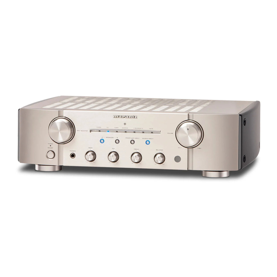
PM8004
PM-KI-PEARL-LITE
Copyright 2010 D&M Holdings Inc. All rights reserved.
WARNING: Violators will be prosecuted to the maximum extent possible.
PM8004 /
PM-KI-PEARL-LITE /
Integrated Amplifier
K1SG/U1B
N1SG/N1B
N2SG/N2B
s
Ver. 2
Please refer to the
MODIFICATION NOTICE.
Advertisement
Table of Contents


Need help?
Do you have a question about the PM8004 and is the answer not in the manual?
Questions and answers