Advertisement
Quick Links
Four-channel, differential input, DAQ front-end circuit with
Victor Salomon
Feature
Number of channels
Data rate
Voltage input range
Current input range
Voltage accuracy
Current accuracy
Design Description
This circuit design describes how to use an
amplifier (PGA) to make voltage and current measurements on various ranges.
This circuit can be used in applications such as
concentrators,
lab and field
applications. Thermocouples and RTD are also common temperature sensors used in similar applications.
For more information about making precision ADC measurements with a variety of RTD wiring
configurations, see the
+
V
= ± 10V
IN
-
+
V
= ± 10V
IN
-
+
= 0 to 20 mA
I
IN
(V = 0 to 5V)
-
+
I
= 0 to 20 mA
IN
(V = 0 to 5V)
-
SBAA386 – December 2019
Submit Documentation Feedback
configurable voltage and current inputs
Power Supplies
AVDD
5.0V
instrumentation, and other
A Basic Guide to Thermocouple Measurements Application
15 V
-15 V
0.1 F
Optional
TVS3300
Input Filter
TVS Protection
VDD
VSS
210
1 k
S1A
MUX509
1 nF
10 nF
1 nF
S1B
210
1 k
210
1 k
S2A
1 nF
10 nF
1 nF
S2B
210
1 k
210
1 k
S3A
1 nF
10 nF
1 nF
S3B
210
1 k
210
1 k
S4A
1 nF
10 nF
1-of-4
Decoder
1 nF
S4B
210
1 k
GND
Four-channel, differential input, DAQ front-end circuit with configurable
Copyright © 2019, Texas Instruments Incorporated
Analog Engineer's Circuit: Data
Value
4
≤ 10
±10.0
0 to 20
0.05 typical | 0.10 maximum
0.10 typical | 0.20 maximum
HV-AVDD
15.0V
ADS125H02
with integrated reference and programmable gain
analog input modules
factory automation
15 V
-15 V
0.1 F
0.1 F
0.1 F
1 F
TVS3300
HV_AVDD
HV_AVSS
AVDD
ADS125H02
Supply
Read
Temp
Sensor
DA
AIN0
DB
AIN1
AINCOM
MUX
A0
GPIO0
A1
GPIO1
GPIO
EN
GPIO2
AGND
DGND
Converters
SBAA386 – December 2019
Units
Differential channels
kSPS
Volts
mA
%FS
%FS
HV-AVSS
–15.0V
for PLCs, avionics
remote data
and
test and measurement
Report.
5 V
5 V
1 F
1 F
10 F
DVDD
REFOUT
REFP0
REFP1
2.5-V
REF
PGA Gain Options
Reg. MODE4 - GAIN[3:0]
0000: 0.125
0110: 4
REF MUX
0001: 0.1875
0111: 8
0010: 0.25
1000: 16
0011: 0.5
1001: 32
BUF
0100: 1
1010: 64
0101: 2
1011: 128
24-Bit
PGA
û ADC
CAPP
CAPN
BYPASS
1 F
1 nF C0G
voltage and current inputs
1
Advertisement

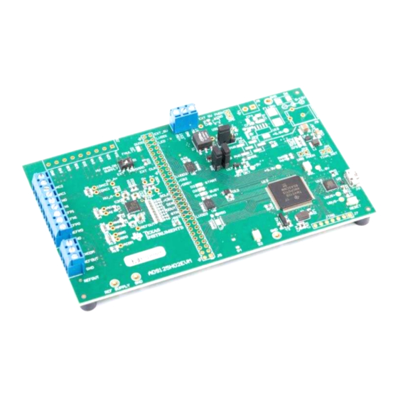
Related Manuals for Texas Instruments ADS125H02


Summary of Contents for Texas Instruments ADS125H02
- Page 1 (V = 0 to 5V) Decoder 1 nF GPIO2 AGND DGND CAPP CAPN BYPASS 1 nF C0G SBAA386 – December 2019 Four-channel, differential input, DAQ front-end circuit with configurable voltage and current inputs Submit Documentation Feedback Copyright © 2019, Texas Instruments Incorporated...
- Page 2 AVDD to the ground plane. Connect a 1.0-µF capacitor from DVDD to the ground plane. Connect a 1.0-µF capacitor from BYPASS to the ground plane. For details on power supply recommendations, see the ADS125H02 ±20-V Input, 2-Channel, 40- kSPS, 24-Bit, Delta-Sigma ADC With PGA and Voltage Reference Data Sheet.
- Page 3 0.25V / V Voltage 2.5V ± 5.0V IN _ FSR Gain 0.50V / V Current 2.5V SBAA386 – December 2019 Four-channel, differential input, DAQ front-end circuit with configurable voltage and current inputs Submit Documentation Feedback Copyright © 2019, Texas Instruments Incorporated...
- Page 4 HV_AVSS 6. GPIO configuration: The ADS125H02 device provides four GPIO pins (GPIO0–GPIO4), two GPIOs are available on dedicated pins and two GPIOs are multiplexed functions with an external reference (REFP1 and REFN1). The GPIO input and output levels are referred to AVDD and AGND, so in this case the logic output levels are set to 5.0V.
-
Page 5: Register Settings
Digital low-pass filters are essential to the functionality of a delta-sigma ADC, which relies on oversampling and noise shaping to push quantization noise out of band. There are a variety of options for digital filters available in the ADS125H02 device. When choosing a digital filter, consider the following tradeoffs: •... -
Page 6: Pseudocode Example
The dedicated DRDY pin indicates the availability of new conversion data. Pseudocode is shown without the use of the STATUS byte and CRC data verification. Download the ADS125H02 Example C Code from the ADS125H02 product folder or access it directly with the following... - Page 7 // Using gain of 0.50 V/V for channels 3 & 4 VoltageReading = (LSBsize * signedValue); If (channelNumber > 2) CurrentReading = (VoltageReading / BurdenResistance); SBAA386 – December 2019 Four-channel, differential input, DAQ front-end circuit with configurable voltage and current inputs Submit Documentation Feedback Copyright © 2019, Texas Instruments Incorporated...
- Page 8 TI's comprehensive circuit library. Power Supply Reference Designs The ADS125H02 device requires three analog power supplies (high-voltage supplies HV_AVDD and HV_AVSS, and low-voltage analog supply AVDD) and a digital power supply (DVDD). This circuit assumes a bipolar supply (±15.0 V) for HV_AVDD and HV_AVSS, and a 5.0-V supply. The following table shows there are specifications for three reference designs that could be used to provide the power supplies from a 24.0 V nominal input voltage.
-
Page 9: Important Notice
TI products. TI’s provision of these resources does not expand or otherwise alter TI’s applicable warranties or warranty disclaimers for TI products. TI objects to and rejects any additional or different terms you may have proposed. IMPORTANT NOTICE Mailing Address: Texas Instruments, Post Office Box 655303, Dallas, Texas 75265 Copyright © 2022, Texas Instruments Incorporated...
Need help?
Do you have a question about the ADS125H02 and is the answer not in the manual?
Questions and answers