Table of Contents
Advertisement
Quick Links
UM_2111_PL12_2111_034836
User manual for TDM3883 evaluation board
3 A synchronous buck voltage regulator with integrated inductor
About this document
Scope and purpose
The TDM3883 3 A point-of-load (POL) module is an easy-to-use, fully integrated and highly efficient DC-DC
module. The module's pulse width modulation (PWM) controller, MOSFETs and inductor make TDM3883 a
space-efficient solution, providing accurate power delivery. The TDM3883 employs an enhanced stability
engine that makes it stable with ceramic capacitors without compensation.
This user manual contains the schematic and bill of materials (BOM) for the EVAL_TDM3883_3.3Vout
engineering evaluation board. The manual describes operation and use of the evaluation board itself. Detailed
application information for TDM3883 is available in the TDM3883 datasheet.
Intended audience
This document is intended as a guide for design engineers evaluating the performance of TDM3883 with the
engineering EVAL_TDM3883_3.3Vout demo board.
Table of contents
About this document ....................................................................................................................... 1
Scope and purpose ......................................................................................................................... 1
Intended audience .......................................................................................................................... 1
Table of contents ............................................................................................................................ 1
1
Board information .................................................................................................................. 2
1.1
Board picture and overview .................................................................................................................... 2
1.2
Board features ......................................................................................................................................... 2
1.3
Connections and operating instructions ................................................................................................ 3
1.4
Power-on procedure ............................................................................................................................... 3
1.5
PCB layout ............................................................................................................................................... 4
1.6
Schematic ................................................................................................................................................ 7
1.7
Bill of materials ........................................................................................................................................ 8
2
Typical operating waveforms .................................................................................................. 9
2.1
P
= 5 V .................................................................................................................................................... 9
2.2
P
= 12 V ................................................................................................................................................ 11
Revision history............................................................................................................................. 17
User Manual
www.infineon.com/optimos-ipol
Please read the Important Notice and Warnings at the end of this document
page 1 of 18
V 1.0
2022-04-28
Advertisement
Table of Contents

Related Manuals for Infineon TDM3883


Summary of Contents for Infineon TDM3883
-
Page 1: Table Of Contents
The manual describes operation and use of the evaluation board itself. Detailed application information for TDM3883 is available in the TDM3883 datasheet. Intended audience This document is intended as a guide for design engineers evaluating the performance of TDM3883 with the engineering EVAL_TDM3883_3.3Vout demo board. Table of contents About this document ........................ -
Page 2: Board Information
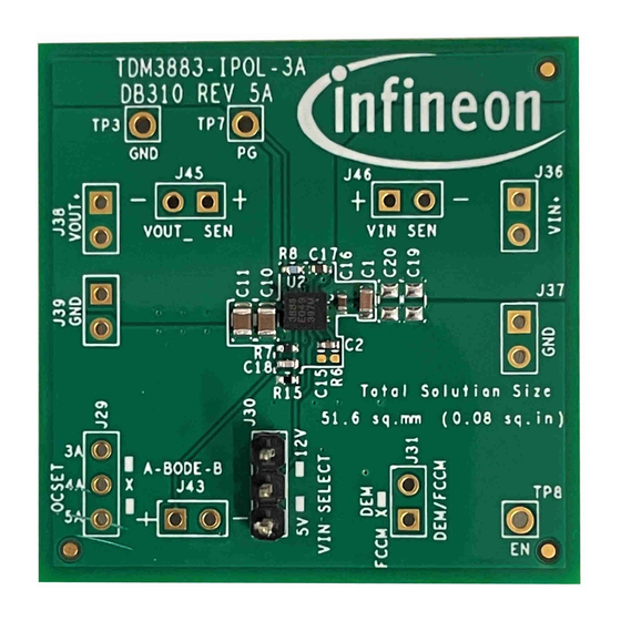
UPUT APACITORS IN [+] OUT [+] MEASUREMENT Figure 1 TDM3883 evaluation board, dimensions (width x length x thickness) = 40 mm x 40 mm x 1.5 mm Board features • = 12 V, V = 3.3 V, I = 0 A to 3 A •... -
Page 3: Connections And Operating Instructions
Connections and operating instructions The TDM3883 demo board allows dual configuration +12 V or +5 V for the input power and can deliver up to 3 A load current. The operation modes and overcurrent protection (OCP) limits can be selected through jumpers. -
Page 4: Pcb Layout
1.5 oz. plating. Inner layers use 2 oz. copper. The PCB thickness is 0.062 in. Layer stack-up is top – GND1 – GND2 – signal – GND3 – bottom. TDM3883 and other major power components are mounted on the top side of the board. Figure 2 Layer stack-up –... - Page 5 User manual for TDM3883 evaluation board 3 A synchronous buck voltage regulator with integrated inductor Board information Figure 3 Layer stack-up – signal (top) and GND 1 (bottom) User Manual 5 of 18 V 1.0 2022-04-28...
- Page 6 User manual for TDM3883 evaluation board 3 A synchronous buck voltage regulator with integrated inductor Board information Figure 4 GND 2 (top) and GND 3 (bottom) User Manual 6 of 18 V 1.0 2022-04-28...
-
Page 7: Schematic
User manual for TDM3883 evaluation board 3 A synchronous buck voltage regulator with integrated inductor Board information Schematic Figure 5 Schematic of the TDM3883 evaluation board User Manual 7 of 18 V 1.0 2022-04-28... -
Page 8: Bill Of Materials
User manual for TDM3883 evaluation board 3 A synchronous buck voltage regulator with integrated inductor Board information Bill of materials Table 3 Bill of materials Part Qty. reference Value Manufacturer Part number Description Ceramic capacitor, 10 µF, 0603, 25 V, 10 µF... -
Page 9: Typical Operating Waveforms
User manual for TDM3883 evaluation board 3 A synchronous buck voltage regulator with integrated inductor Typical operating waveforms Typical operating waveforms = 5 V Figure 6 Start-up, P = 5 V, V = 2.5 V, I = 0 A, FCCM. Ch1 = V... - Page 10 User manual for TDM3883 evaluation board 3 A synchronous buck voltage regulator with integrated inductor Typical operating waveforms Figure 8 Load regulation, P = 5 V, V = 2.5 V Note: Section 2.1, P = 5 V. R is changed from 6.98 kΩ to 9.76 kΩ to configure V = 2.5 V.
-
Page 11: Vin
User manual for TDM3883 evaluation board 3 A synchronous buck voltage regulator with integrated inductor Typical operating waveforms = 12 V Figure 9 Start-up, P = 12 V, V = 3.3 V, I = 0 A, FCCM. Ch1 = V... - Page 12 User manual for TDM3883 evaluation board 3 A synchronous buck voltage regulator with integrated inductor Typical operating waveforms Figure 11 Start-up pre-bias (1 V), P = 12 V, V = 3.3 V, I = 0 A, FCCM. Ch1 = V...
- Page 13 User manual for TDM3883 evaluation board 3 A synchronous buck voltage regulator with integrated inductor Typical operating waveforms Figure 13 Recover from a shorted V = 12 V, V = 3.3 V, I = 3 A, FCCM. Ch1 = V...
- Page 14 User manual for TDM3883 evaluation board 3 A synchronous buck voltage regulator with integrated inductor Typical operating waveforms Figure 15 Transient response, P = 12 V, V = 3.3 V, I = 0 A to 3 A, FCCM. Ch1 = V , Ch2 = I Slew rate = 5 A/µS...
- Page 15 User manual for TDM3883 evaluation board 3 A synchronous buck voltage regulator with integrated inductor Typical operating waveforms Figure 16 Load regulation, P = 12 V, V = 3.3 V Figure 17 Efficiency, P = 12 V, V = 3.3 V...
- Page 16 User manual for TDM3883 evaluation board 3 A synchronous buck voltage regulator with integrated inductor Typical operating waveforms Room temperature, no airflow. Board data: TDM3883 EVB DB310 REV 5A Dimensions (width x length x thickness) = 40 mm x 40 mm x 1.5 mm...
-
Page 17: Revision History
User manual for TDM3883 evaluation board 3 A synchronous buck voltage regulator with integrated inductor Revision history Revision history Document version Date of release Description of changes V 1.0 2022-04-28 Initial release User Manual 17 of 18 V 1.0 2022-04-28... - Page 18 Do you have a question about this Except as otherwise explicitly approved by Infineon information given in this application note. Technologies in a written document signed by...
Need help?
Do you have a question about the TDM3883 and is the answer not in the manual?
Questions and answers