Table of Contents
Advertisement
Quick Links
UM11768 BYLink multiprocessor
demo board user manual
Rev. 1 — 7 April 2022
Document information
Information
Content
Keywords
FS8500, PF5024, PF5020, PMIC, BYLINK, power sequencing, safety, fault
management, multiprocessor, camera application, ADAS
Abstract
The BYLink multiprocessor demo board user guide is intended for engineers
involved in the evaluation or development of a BYLink system involving an
NXP PMIC, such as one from the FS8500 device family or the PF502x device
family.
Revision history
Rev
Date
1
20220407
Description
Initial version.
User manual
Advertisement
Table of Contents

Related Manuals for NXP Semiconductors UM11768


Summary of Contents for NXP Semiconductors UM11768
- Page 1 UM11768 BYLink multiprocessor demo board user manual Rev. 1 — 7 April 2022 User manual Document information Information Content Keywords FS8500, PF5024, PF5020, PMIC, BYLINK, power sequencing, safety, fault management, multiprocessor, camera application, ADAS Abstract The BYLink multiprocessor demo board user guide is intended for engineers...
-
Page 2: Introduction
Finding kit resources and information on the NXP website NXP Semiconductors provides online resources for this evaluation board and its supported device(s) on http://www.nxp.com The information page for the BYLink Multiprocessor demo board is at https://www.nxp.com/products/product-information/... -
Page 3: Software
NXP Semiconductors UM11768 BYLink multiprocessor demo board user manual 3.4 Software The following software must be installed on the PC workstation prior to using the BYLink Multiprocessor demo board. • BYLink NXP GUI installation package Getting to know the hardware 4.1 Kit overview... - Page 4 NXP Semiconductors UM11768 BYLink multiprocessor demo board user manual Figure 1. Jumper and switch details Table 1. Jumper and switch details Name Function Pin number Jumper/pin function Default Debug Mode "1-2" DBG voltage 5V "2-3" "2-3" DBG voltage to GND (default) AMUX "1-2"...
-
Page 5: Schematic, Board Layout And Bill Of Materials
NXP Semiconductors UM11768 BYLink multiprocessor demo board user manual Table 1. Jumper and switch details ...continued "2-3" WDI short to high Position Function Description Default "1-2" Wake1 closed Wake1 pin connected to VSUP "2-3" "2-3" Wake1 open Wake1 pin not connected to VSUP (default) -
Page 6: References
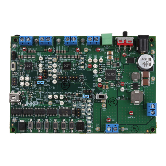
NXP Semiconductors UM11768 BYLink multiprocessor demo board user manual Figure 2. BYLink demo board picture References [1] Detailed information on https://www.nxp.com/products/product-information/product-programs/bylink-system- BYlink power-platform:BYLINKl UM11768 All information provided in this document is subject to legal disclaimers. © NXP B.V. 2022. All rights reserved. -
Page 7: Legal Information
NXP Semiconductors. In the event that customer uses the product for design-in and use in In no event shall NXP Semiconductors be liable for any indirect, incidental, automotive applications to automotive specifications and standards, punitive, special or consequential damages (including - without limitation - customer (a) shall use the product without NXP Semiconductors’... - Page 8 NXP Semiconductors UM11768 BYLink multiprocessor demo board user manual Tables Tab. 1. Jumper and switch details .........4 Figures Fig. 1. Jumper and switch details .........4 Fig. 2. BYLink demo board picture .......6 UM11768 All information provided in this document is subject to legal disclaimers.
-
Page 9: Table Of Contents
NXP Semiconductors UM11768 BYLink multiprocessor demo board user manual Contents Introduction ............2 Finding kit resources and information on the NXP website ..........2 Collaborate in the NXP community ....2 Getting ready ............2 Kit contents ............2 Additional hardware ........... 2 Windows PC workstation ........2 Software .............3...
Need help?
Do you have a question about the UM11768 and is the answer not in the manual?
Questions and answers