
Related Manuals for Panasonic RS-DV290EG


Summary of Contents for Panasonic RS-DV290EG
- Page 1 AD0303010C8 Cassette Deck RS-DV290EG Colour (S)..Silver Type SPECIFICATIONS...
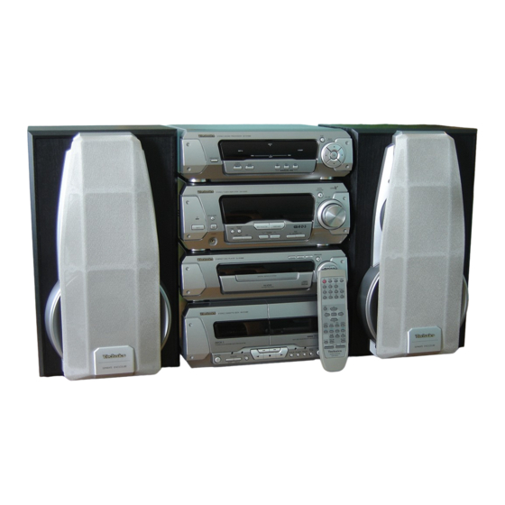
- Page 2 1. Note Refer to the service manual for Model No. SA-EH590EG, SA-EH590EP (Order No. AD0302008C8) for information on Accessories and Packaging. 2. Location of Controls 3. Operation Checks and Component Replacement / Procedures - This section describes procedures for checking the operation of the major printed circuit boards and replacing the main components.
- Page 4 - Check the operation P.C.B. as shown below. 3.3. Replacement for the motor ass’y, capstan belt and winding belt - Follow the (Step 1) - (Step 3) of item 3.1.
- Page 5 - Follow the (Step 1) - (Step 7) of item 3.2.
- Page 8 3.4. Replacement for the components parts on the mechanism P.C.B. - Follow the (Step 1) - (Step 3) of item 3.1. - Follow the (Step 1) - (Step 7) of item 3.2. - Follow the (Step 1) - (Step 4) of item 3.3.
-
Page 9: Replacement For The Pinch Roller Ass'y And Head Block
3.5. Replacement for the pinch roller ass’y and head block - Follow the (Step 1) - (Step 3) of item 3.1. - Follow the (Step 1) - (Step 7) of item 3.2. - Follow the (Step 1) - (Step 5) of item 3.3. 3.6. - Page 10 3.7. Replacement for the cassette holder - Follow the (Step 1) - (Step 3) of item 3.1. - Follow the (Step 1) - (Step 11) of item 3.2.
-
Page 11: To Supply Power Source
4. To Supply Power Source This unit is designed to operate on power supplied from system connected. / When a component requires service, use the system connections to supply power source. / For system connections, refer to Fig.4-1. Fig. 4-1. 5. -
Page 12: Selecting Service Mode
5.2. Selecting service mode 1. Turn on the power to the unit. 2. Make sure that no tape is inserted in the cassette deck. (Service mode cannot be selected with a tape inserted in the cassette deck.) 3. Press the DOLBY NR button for about 2 seconds, and keep pressing it, also press the STOP button for about 2 seconds. - Page 13 pressed, the fault items are displayed in sequence. Fig. 5-2. Table 5-1. FL display Symptom Cause Cassette deck does not operate correctly. Faulty cassette deck mechanism mode switch (Deck 1: S951, Deck 2: S971), plunger and capstan motor. / (Check and replace) Unit does not record or the unit goes into Faulty erasure prevention tabs detect switch recording mode even when the erasure...
- Page 14 cassette holder. Refer to Fig. 5-3. 3. Insert a metal tape into the Deck 2 with an intact erasure prevention tab on the right side. 4. Close the Deck 2 cassette holder. 5. Press the Fast forward button. Refer to Fig.
-
Page 15: Schematic Diagram Notes
5.5. Exiting service mode 1. Press the STOP button for more than 5 seconds. (Diagnostic contents stored in memory for both Deck 1 and 2 are erased.) 2. Remove the cassette tape from the cassette holder. 3. Turn off the unit. 6. - Page 16 Fast forward, TPS switch ( S907: Forward side playback switch ( S909: Reverse side playback switch ( S910: Rewind, TPS switch ( S911: Reverse mode switch / (REV MODE) S912: Deck 1/deck 2 select switch / (DECK 1/2) S913: Counter display switch / (COUNTER DISPLAY) S914: Counter reset switch / (COUNTER RESET) S915:...
- Page 17 S974: Deck 2 reverse side record prevention tab detect switch S975: Deck 2 forward side record prevention tab detect switch S976: Deck 2 METAL tape detect switch VR101: Deck 1 playback gain adjustment VR / (R ch) VR102: Deck 2 playback gain adjustment VR / (L ch) VR103: Deck 2 playback gain adjustment VR / (R ch) VR104:...
- Page 18 When replacing any of components, be sure to use only manufacturer’s specified parts shown in the parts list. - The supply part number is described alone in the replacement parts list. - Caution! IC and LSI are sensitive to static electricity. Secondary trouble can be prevented by taking care during repair.
- Page 19 Terminal Function Name Power supply terminal VREF Reference voltage input GND terminal O Muting control signal output O Deck 1 solenoid control signal output O Deck 1 motor drive control signal output HALT Power failure detect signal input Serial communication request signal input Serial communication complete signal input...
-
Page 20: Measurements And Adjustments
Terminal Function Name O Deck 2 solenoid control signal output O Deck 2 motor drive control signal output 31 ENC/DEC O Dolby NR record/playback mode select signal output 32 DOLBY O Dolby NR ON/OFF control signal ON/OFF output E CS EEPROM chip select signal output (Not used, open) - Page 21 - AF Oscillator - Test tape - Head azimuth adjustment (8 kHz, -20 dB): QZZCFM - Tape speed adjustment (3 kHz, -10 dB): QZZCWAT - Playback gain adjustment (315 Hz, 0 dB): QZZCFM - Recording/playback frequency response check: QZZCFM / (315 Hz, -20 dB, 12.5 kHz~63 Hz, -20 dB) QZZCRA4 (Normal blank tape) QZZCRX2 (CrO2 blank tape) QZZCRZ6 (Metal blank tape)
- Page 22 13.4. Tape speed adjustment / (Deck 1/2) Note: When connecting the unit to other system components for test, short the section between the test point TP604 and TP609 and turn on the entire system. (The unit is set to the TEST mode, and either Deck 1 or Deck 2 indicatorwill blink.) Normal speed (Standard value: 3000 ±...
- Page 23 [Standard value:265 mV ~ 300 Fig. 13-4. 13.6. Erase current confirmation (Deck 2) 1. Connect the measuring instrument as shown in Fig. 13-5. 2. Insert the blank tape into Deck 2, and press the Record pause button. 3. Check if the output at this time between the erase current confirmation point TP301 and TP302 (the output on both edged of R313) is within the standard value shown below.
- Page 24 output as a reference (0 dB). 3. Confirm the playback frequency response is within the range shown in Fig. 13-7. Fig. 13-6. Fig. 13-7. 13.8. Recording/playback / frequency response and gain check (Deck 2) 13.8.1. Normal tape check 1. Connect the measuring instrument as shown in Fig.
- Page 25 13.8.2. CrO2/Metal tape check 1. Connect the measuring instrument as shown in Fig. 13-8. 2. Insert a CrO2/Metal tape into Deck 2. 3. Record signals at 50 Hz, 100 Hz, 200 Hz, 500 Hz, 1 kHz, 2 kHz, 10 kHz and 12.5 kHz (28 mV). 4.
- Page 26 Fig. 13-11. 14. Checking Procedure for Self-operation of Cassette Mechanism Ass’y - This procedure describes simple methods independent of mechanism controller or governor circuit. 14.1. Operation Check Providing with Cassette Tape 1. Push up the EJECT lever with rubber band. (Refer to Fig.
- Page 27 Repeat the above operation to FWD PLAY mode. Note: Incorrect duration for power supply may be operated to other mode. 14.1.1. Connection Diagram Between the Mechanism Ass’y and Power Supply / (MOTOR and Plunger) Fig. 14-1. 14.1.2. Detail View of EJECT Lever / (EJECT lever fixed by rubber band, Plunger rib operation) Fig.
-
Page 28: Replacement Parts List
15. Replacement Parts List Notes: - Important safety notice: Components identified by mark have special characteristics important for safety. Furthermore, special parts which have purposes of fire-retardant (resistors), high-quality sound (capacitors), low-noise (resistors), etc. are used. When replacing any of components, be sure to use only manufacture’s specified parts shown in the parts list. - Page 29 Ref. No. Part No. Part Name & Description Remarks RKM0392-S1 CABINET RHD30007-1S SCREW XTBS3+10JFZ1 SCREW RGR0287A-P REAR PANEL RKA0105-K RUBBER RKA0106-N FOOT RING RMN0539 CABLE HOLDER RDG0129-1 DAMPER GEAR REX0966-1 WIRE ASS'Y RGB0025-A TECHNICS BADGE RGK1131-2S ORNAMENT(L) RGK1132-2S ORNAMENT(R) RGL0441-Q PANEL LIGHT REZ1194 WIRE ASS'Y...
- Page 30 Ref. No. Part No. Part Name & Description Remarks RMR0909-X PCB HOLDER RED0037 HEAD BLOCK ASS'Y / (R/P) L1AA00000008 101-1 RHD17015 SCREW RED0038 HEAD BLOCK ASS'Y / (P.B) 102-1 RHD17015 SCREW RDG0300 REEL TABLE BASE RDG0301 GEAR RDK0026 GEAR RDV0033-4 BELT1 RDV0034-1 BELT2...
- Page 31 Ref. No. Part No. Part Name & Description Remarks C129 ECEA1AKS220 10V 22U C130 F2A1C101A133 16V 100U C131-34 ECJ2VB1H471K 50V 470P C135,36 ECA1HAK010XI 50V 1U C137 ECEA1HKS0R1 50V 0.1U C138 F1J1E4730004 25V 0.047U C139 ECEA0JKS470 6.3V 47U C140 ECEA1CKS100 16V 10U C141 ECA1HAK010XI 50V 1U...
- Page 32 Ref. No. Part No. Part Name & Description Remarks CS971 RJU071H09M CONNECTOR(9P) K1KB09C00001 D101,02 MA2J11100L DIODE D301 MA2J11100L DIODE D606 MAZ40560MF DIODE D651,52 MA165TA5 DIODE MA2C16500E D701 MA2J11100L DIODE D705,06 MA2J11100L DIODE D707 MA4051M DIODE MAZ40510M D708-10 MA2J11100L DIODE D904 MA2J11100L DIODE D905...
- Page 33 Ref. No. Part No. Part Name & Description Remarks Q902-04 DTC143EUT106 TRANSISTOR B1GBCFGG0006 R101,02 ERJ6GEYJ562V 1/10W 5.6K R103,04 ERJ6GEYJ104V 1/10W 100K R105,06 ERJ6GEYJ334V 1/10W 330K R107,08 ERJ6GEYJ103V 1/10W 10K R109,10 ERJ6GEYJ102V 1/10W 1K R111 ERJ6GEYJ820V 1/10W 82 D0GD820JA012 R112 ERJ8GEYJ820V 1/8W 82 R113 ERJ6GEYJ123V...
- Page 34 Ref. No. Part No. Part Name & Description Remarks R305 ERJ6GEYJ183V 1/10W 18K R306 ERJ6GEYJ333V 1/10W 33K R307 ERDS1FJ2R2 1/2W 2.2 R308 ERJ6GEYJ102V 1/10W 1K R309-11 ERJ6GEYJ472V 1/10W 4.7K R313 ERDS2TJ1R0 1/4W 1.0 R602 ERQ16NKWR33E 1/6W 0.33 R603 ERD2FCG100 1/4W 10 R604 ERJ6GEYJ331V 1/10W 330...
-
Page 35: Cabinet Parts Location
Ref. No. Part No. Part Name & Description Remarks R903 ERJ6GEYJ152V 1/10W 1.5K R904 ERJ6GEYJ182V 1/10W 1.8K R905 ERJ6GEYJ222V 1/10W 2.2K R906 ERJ6GEYJ332V 1/10W 3.3K D0GD332JA003 R908 ERJ6GEYJ122V 1/10W 1.2K D0GD122JA003 R909 ERJ6GEYJ152V 1/10W 1.5K R910 ERJ6GEYJ182V 1/10W 1.8K R911 ERJ6GEYJ222V 1/10W 2.2K R914... -
Page 36: Mechanism Parts Location
17. Mechanism Parts Location... -
Page 38: Schematic Diagram For Printing With Letter Size
18. Schematic Diagram for printing with letter size F0302KH... - Page 39 OPERATION CIRCUIT :POSITIVE VOLTAGE LINE :PLAYBACK SIGNAL LINE Q901 S907 DTA143EUT106 D907 SML79455C LED DRIVE Q903 R916 DTC143EUT106 S912 S906 LED DRIVE(FWD) (DECK 1/2) 4.2V S911 S905 (REV MODE) (DOLBY NR) D905 SML79455C R914 Q904 S910 S904 ( REC PAUSE) DTC143EUT106 R915 LED DRIVE(REV)
-
Page 40: Main Circuit
MAIN CIRCUIT :POSITIVE VOLTAGE LINE : RECORDING SIGNAL LINE : PLAYBACK SIGNAL LINE R101 C123 5.6K 25V4.7 R157 9.6V C150 (0.2V) Q101 C143 C115 10V100 DECK1 CP101 470P 470P 2SJ164RTA HEAD SELECT (REC:ON) C117 330P PLAYBACK HEAD C129 R117 R725 10V22 2.2K IC101... - Page 41 : PLAYBACK SIGNAL LINE DOLBY R725 2.2K C207 270P C203 R209 R211 R221 C225 25V4.7 L201 25V4.7 C205 50V1 C218 R237 R220 50V0.1 (9.6V) 0.1V DOLBY ON : 0V (0.1V) 4.8V 9.6V 4.7V 4.7V 4.6V 4.7V 0.4V 4.8V 9.6V ON/OFF IC201 CXA1552M-T4 DOLBY B NR...
-
Page 42: Mechanism Circuit (Deck1)
MAIN CIRCUIT :POSITIVE VOLTAGE LINE : RECORDING SIGNAL LINE : PLAYBACK SIGNAL LINE Q807 Q809 Q810 Q808 2SB621ARSTA DTC143EUT106 DTC143EUT106 2SB621ARSTA SOLENOID DRIVE SOLENOID DRIVE SOLENOID DRIVE SOLENOID DRIVE 10.3V R802 R823 R824 R812 10.3V 10.3V 10.3V 10.2V 10.2V 10.3V Q803 Q805 2SD592ARSTA... - Page 43 LAYBACK SIGNAL LINE 4.8V Q701,703 2SD1819ARTX R738 R747 5ms. 2V/DIV. INTERFACE 4.8V R704 16 ms. 1.9V 4.7K 0.1V 3.6V Q701 R708 16ms. 1.8V 4.7K 1.2V R737 R736 Q703 F=8MHz R705 L701 R711 10 H 100K R722 0.2V C706 0.6V 50V3.3 1 2 3 4 5 6 7 8 9 10 11 12 13 14 15 16 17 18 19 20 21 CN901 X701...
-
Page 44: Operation Circuit
OPERATION CIRCUIT :POSITIVE VOLTAGE LINE :PLAYBACK SIGNAL LINE Q901 S907 D907 DTA143EUT106 SML79455C LED DRIVE Q903 R916 DTC143EUT106 S912 S906 LED DRIVE(FWD) ( DECK 1/2 ) 4.2V S911 S905 ( REV MODE ) ( DOLBY NR ) D905 SML79455C R914 Q904 S910 S904... - Page 46 BA7755AF CXA1998BQT6 0N2180RLC1 2SD1450RSTA CXA1552M-T4 16PIN MC14066BFEL 14PIN M38503M2406F 42PIN No.1 2SB621ARSTA 2SD1819ARTX 2SC3940AQSTA 2SD2144STA 2SJ164QTA 2SJ164RTA 2SD592ARSTA 2SD1328STXRA DTA143EUT106 DTC114EUT106 DTC143EUT106 DTC144EUT106 MA165TA MA4051MTA SML79455C MA111TX MA4056MTA Cathode Cathode Anode Cathode Anode Cathode Anode Anode Anode...
-
Page 47: Earth Terminal P.c.b
[DECK 2] [DECK 1] EARTH TERMINAL P.C.B. R/P HEAD, PLAYBACK ERASE HEAD HEAD W601 1 . . . 5 1 . . . 5 1 . 5 1 . 5 W601 CP101 CP102 MAIN P.C.B. To DVD CHANGER, CD CHANGER, CD PLAYER &... - Page 49 MC14066BFEL NOTES : PLAYBACK SIGNAL LINE IC202 : RECORDING SIGNAL LINE SIGNAL CONT. ) indicates pin No. Right channel. To DVD CHANGER, CD CHANGER, CD PLAYER CXA1552M-T4 BLOCK DIAGRAM & IC201 SOUND PROCESSOR DOLBY B NR BLOCK DIAGRAM Q108 MC14066BFEL (11) CN601 SWITCH-...
- Page 50 Note: This printed circuit board diagram may be modified at any time with the development of new technology. EARTH TERMINAL P.C.B. OPERATION P.C.B. MAIN P.C.B. W601 Q303 Q306 L301 E C B S901 Q305 C302 OPEN) Q301 C303 E C B (REP2827E-M) Q304 S904...
- Page 51 MAIN CIRCUIT :POSITIVE VOLTAGE LINE : RECORDING SIGNAL LINE : PLAYBACK SIGNAL LINE R101 C123 5.6K 25V4.7 R157 9.6V C150 Q101 (0.2V) C143 C115 10V100 DECK1 CP101 470P 470P 2SJ164RTA HEAD SELECT (REC:ON) C117 330P DOLBY PLAYBACK HEAD C129 R117 R725 10V22 2.2K...
- Page 52 MAIN CIRCUIT :POSITIVE VOLTAGE LINE : RECORDING SIGNAL LINE : PLAYBACK SIGNAL LINE 4.8V Q701,703 Q807 Q809 Q810 Q808 2SD1819ARTX R738 R747 2SB621ARSTA DTC143EUT106 DTC143EUT106 2SB621ARSTA 5ms. 2V/ DIV. INTERFACE SOLENOID DRIVE SOLENOID DRIVE SOLENOID DRIVE SOLENOID DRIVE 10.3V 4.8V R802 R823 R824...
Need help?
Do you have a question about the RS-DV290EG and is the answer not in the manual?
Questions and answers