Table of Contents
Advertisement
Quick Links
One Technology Way • P.O. Box 9106 • Norwood, MA 02062-9106, U.S.A. • Tel: 781.329.4700 • Fax: 781.461.3113 • www.analog.com
Evaluating the
ADM2463E
FEATURES
Simplified evaluation of the
signal isolated, 500 kbps, full duplex RS-485 transceiver
2-layer PCB compliant to EN 55032 Class B radiated
emissions
Footprint for standard full duplex, 16-lead, SOIC_W package
with >8 mm creepage and clearance
On-board
ADP7104
LDO regulators with jumper options for
simplified evaluation in multiple supply configurations
Flexible, low voltage V
supply rail for interfacing with I/O
DD1
nodes as low as 1.7 V
Wide bus voltage V
supply rail from 3 V to 5.5 V
DD2
IEC 61000-4-2 ESD protection on the A pin, B pin, Y pin, and
Z pin
≥±12 kV contact discharge and ≥±15 kV air discharge
SMA connector for TxD input signal
Optional on-board
LTC1799
Screw terminal blocks for connecting power, digital, and
RS-485 signals
Jumper-selectable enable and disable for digital input signals
Resistors and footprints for termination and loopback test
Test points for measuring all signals
EVALUATION KIT CONTENTS
EVAL-ADM2463EEBZ/EVAL-ADM2763EEBZ
EQUIPMENT NEEDED
Oscilloscope
Signal generator
3 V to 5.5 V secondary side supply
1.7 V to 5.5 V primary side supply
DOCUMENTS NEEDED
ADM2463E
data sheet
ADM2763E
data sheet
PLEASE SEE THE LAST PAGE FOR AN IMPORTANT
WARNING AND LEGAL TERMS AND CONDITIONS.
EVAL-ADM2463EEBZ/EVAL-ADM2763EEBZ
and
ADM2763E
Duplex RS-485 Transceivers with ±15 kV IEC ESD
ADM2463E
and
ADM2763E
oscillator for providing TxD signal
500 kbps, 5.7 kV RMS, Signal Isolated, Full
GENERAL DESCRIPTION
The EVAL-ADM2463EEBZ/EVAL-ADM2763EEBZ allow
simplified, efficient evaluation of the
ADM2763E
5.7 kV rms, 500 kbps signal isolated RS-485
transceivers. The functionality of the EVAL-ADM2463EEBZ
and the EVAL-ADM2763EEBZ are the same. Figure 1 shows the
EVAL-ADM2463EEBZ and represents both evaluation boards.
The EVAL-ADM2463EEBZ/EVAL-ADM2763EEBZ come with
options for the evaluation of the
devices in an individual system. Digital and RS-485 bus signals
are easily accessible via the screw terminal blocks on the
evaluation boards. Each digital input can be configured via the
on-board jumper options.
Two on-board
ADP7104
an input voltage of up to 20 V and output a range of selectable
supply voltages to the V
jumper options. The LDO regulators can be bypassed to power
the
ADM2463E
V
supply pins directly from an external power supply.
DD2
The flexible V
DD1
to operate with a digital input/output (I/O) voltage from 1.7 V
to 5.5 V, which enables communication with modern nodes
using either a 1.8 V or 2.5 V power supply. The V
also be supplied from the
Alternative methods can be used to provide the transmit data
input (TxD) signal to the device. An optional
is included on the evaluation boards and can be configured to
provide a clock signal as the TxD digital input within a 10 kHz
to 250 kHz range. A terminal block allows an easy wired
connection to a microcontroller or processor. For optimal signal
integrity, use the on-board Subminiature Version A (SMA)
connector to connect an external data signal.
The evaluation boards have footprints for the
ADM2763E
full duplex, signal isolated, RS-485 transceivers in
a 10.10 mm × 10 mm, 16-lead, standard small outline, wide
body (SOIC_W) package.
For full details on the
ADM2463E
and
conjunction with this user guide when using the EVAL-
ADM2463EEBZ/EVAL-ADM2763EEBZ.
Rev. 0 | Page 1 of 11
ADM2463E
ADM2463E
low dropout (LDO) regulators accept
pin and V
pin, configurable via
DD1
DD2
and
ADM2763E
V
supply pins and
DD1
pin primary side logic supply allows the device
ADP7104
regulated supply.
LTC1799
ADM2463E
and ADM2763E, see the
ADM2763E
data sheets, which must be used in
User Guide
UG-1715
and
and
ADM2763E
pin can
DD1
oscillator
ADM2463E
and
Advertisement
Table of Contents

Related Manuals for Analog Devices EVAL-ADM2463EEBZ


Summary of Contents for Analog Devices EVAL-ADM2463EEBZ
-
Page 1: Features
ADM2763E 5.7 kV rms, 500 kbps signal isolated RS-485 emissions transceivers. The functionality of the EVAL-ADM2463EEBZ Footprint for standard full duplex, 16-lead, SOIC_W package and the EVAL-ADM2763EEBZ are the same. Figure 1 shows the with >8 mm creepage and clearance EVAL-ADM2463EEBZ and represents both evaluation boards. -
Page 2: Table Of Contents
UG-1715 EVAL-ADM2463EEBZ/EVAL-ADM2763EEBZ User Guide TABLE OF CONTENTS Features ....................1 Input and Output Connections ...........5 Evaluation Kit Contents ..............1 Radiated Emissions ...............5 Equipment Needed ................1 Other Board Components............5 Documents Needed ................1 Full Duplex RS-485 Transceivers Loopback Test ......6 General Description ................. -
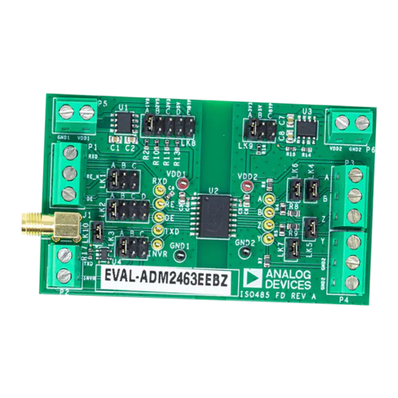
Page 3: Evaluation Board Photograph
EVAL-ADM2463EEBZ/EVAL-ADM2763EEBZ User Guide UG-1715 EVALUATION BOARD PHOTOGRAPH Figure 1. EVAL-ADM2463EEBZ Rev. 0 | Page 3 of 11... -
Page 4: Evaluation Board Hardware
The corresponding labeled test Position E to power the V pin directly from the VDD1 connector. Insert the LK9 jumper into Position C to power the points allow monitoring of the EVAL-ADM2463EEBZ/EVAL- ADM2763EEBZ V and V supply voltages. -
Page 5: Input And Output Connections
Connections to the RS-485 bus are made via the P3 and P4 a 200 mV minimum differential voltage in the bus idle condition screw terminal blocks. The EVAL-ADM2463EEBZ/EVAL- depends on the minimum supply voltage and the termination ADM2763EEBZ have four bus input and output signals: Signal scheme. -
Page 6: Full Duplex Rs-485 Transceivers Loopback Test
ADP7104 LDO regulators that allow flexible power A loopback test can be set up with the EVAL-ADM2463EEBZ/ supply configurations during evaluation. EVAL-ADM2763EEBZ by closing the LK4 and LK5 jumpers. The details of this test are shown in Table 1 and in Figure 2. A... -
Page 7: Iec 61000-4-2 Electrostatic Discharge (Esd) Protection
ADM2463E ADM2763E Pin A, Pin B, The EVAL-ADM2463EEBZ/EVAL-ADM2763EEBZ are tested Pin Y, and Pin Z are subjected to at least 10 positive and 10 and verified to achieve protection against IEC 61000-4-2 ESD to negative single discharges with a 1 sec interval between each ≥±12 kV (contact discharge) and ≥±15 kV (air discharge) on... -
Page 8: Evaluation Board Schematic And Artwork
UG-1715 EVAL-ADM2463EEBZ/EVAL-ADM2763EEBZ User Guide EVALUATION BOARD SCHEMATIC AND ARTWORK Figure 3. EVAL-ADM2463EEBZ/EVAL-ADM2763EEBZ Schematic Rev. 0 | Page 8 of 11... - Page 9 EVAL-ADM2463EEBZ/EVAL-ADM2763EEBZ User Guide UG-1715 Figure 4. EVAL-ADM2463EEBZ/EVAL-ADM2763EEBZ Component Side, Layer 1 Figure 5. EVAL-ADM2463EEBZ/EVAL-ADM2763EEBZ, Layer 2 Figure 6. EVAL-ADM2463EEBZ/EVAL-ADM2763EEBZ, Silkscreen Rev. 0 | Page 9 of 11...
-
Page 10: Ordering Information
UG-1715 EVAL-ADM2463EEBZ/EVAL-ADM2763EEBZ User Guide ORDERING INFORMATION BILL OF MATERIALS Table 4. EVAL-ADM2463EEBZ/EVAL-ADM2763EEBZ Bill of Materials Reference Designator Description Manufacturer Part Number A, B, DE, INVR, RE, Test points, yellow Keystone Electronics 36-5004-ND RxD, TxD, Y, Z C4, C5, C10 Capacitors, 0.1 µF, 0402... - Page 11 By using the evaluation board discussed herein (together with any tools, components documentation or support materials, the “Evaluation Board”), you are agreeing to be bound by the terms and conditions set forth below (“Agreement”) unless you have purchased the Evaluation Board, in which case the Analog Devices Standard Terms and Conditions of Sale shall govern. Do not use the Evaluation Board until you have read and agreed to the Agreement.
Need help?
Do you have a question about the EVAL-ADM2463EEBZ and is the answer not in the manual?
Questions and answers