Table of Contents
Advertisement
Service Manual
•
General Description
Adjustment Procedures
I
Block
Schematic Diagrams
Exploded Views
•
SPECIFICATION
ITEM
•
POWER
RECORDING
SYSTEM
TVTUNER
SYSTEM
RF OUT
SYSTEM
VIDEO
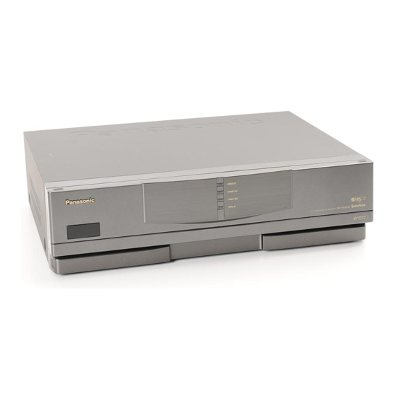
Panasonic
I
Parts List
SPECIFICATION
SOURCE: 220-240V AC 50/60Hz
CONSUMPTION: 41 watts
2 rotary heads, helical scanning system
PAL
UHF:
CH21 ~CH69 (P AL I)
NV-HSlO00B
750 terminated
VHF:
CHE2~CHS3
VHF III: CHM1~CHE12
NV-HSlO00EC
VHF H: CHUl ~CHS41 (PAL B)
UHF:
CH21~CH69 (PAL G)
750 terminated
UHF: 36±6 (PAL I)
NV-HSlO00B
73±3c!B,,, 750 terminated
UHF: 36±4 (PAL G)
NV-HSlO00EC
7 0:::�dBµ, 750 terminated
HEADS: 4 rotary heads
1 pair for SP recording,
playback and trick play (L-R heads)
1 pair for LP recording,
playback and trick play (L' -R' heads)
1 flying erase head
EURO AV (AVl, AV2)
INPUT:
Connectors (21 pin)
1.0Vp-p, 750 unbalanced
S-VIDEO IN (AV3) Connector
Y: 1.0Vp-p, 750 unbalanced
C: 0.3Vp-p, 750 unbalanced
VIDEO IN (AV3)
Connector (Phono type)
1.0Vp-p, 750 unbalancad
OUTPUT: EURO AV (AVl, AV2)
Connectors (21 pin)
1.0Vp-p, 750 unbalanced
S-VIDEO OUT Connector
Y: 1.0Vp-p, 750 unbalanced
C: 0.3Vp-p, 750 unbalanced
VIDEO OUT Connector (Phono type)
1.0Vp-p, 750 unbalanced
Weight and dimensions shown are approximate.
Specifications are subject to change without notice.
Panasonic SI V JISI �:�
NV-HS1 OOO�c
K-M ECHANI ISM
ITEM
HEAD:
1 stationary head (Normal Audio)
2 rotary heads (Hi-Fi 2CH)
INPUT:
EURO AV (AVl, AV2)
Connectors (21 pin)
More than -6c!BV (500mV),
More than l0kO
AUDIO IN (AV3)
Connector (Phono type)
More than -lOdBV (316mV),
More than 47k0
AUDIO
MICROPHONE JACK -70dBV
OUTPUT: EURO AV (AVl, AV2)
Connectors (21 pin)
-6c!BV (500mV), Less than lkO
AUDIO OUT Connector (Phono type)
-Sc!BV (400mV), Less than lkO
HEADPHONE JACK -30dBV, 80
TRACK: 1 track (Normal-mono only)
2 channels (Hi-Fi Sound-Stereo)
TAPE FORMAT
S-VHS, VHS Cassette tape (Tape width 12.7mm)
SP: 23.39 mm/s (PAL), 33.35mm/s (NTSC)
LP: 11.695mm/s (PAL), ll.12mm/s (NTSC)
Record/Playback Time:
TAPE SPEED
SP: 4 hours with 240min. type tape
LP: 8 hours with 240 min. type tape
FF/REW Time:
2.5min. with 180min. type tape
DIMENSIONS
430(W) x 120(H) x 398(D) mm
WEIGHT
7.4kg
1 pc. DIN-RF Cable
1 pc. Infra-red Remote Controller
STANDARD
1 pc. Audio Cables
ACCESSORIES
1 pc. AC Mains Lead
1 pc. EDIT 5 pin Cable
1 pc. S-VIDEO 4P Cable
ORDER NO. VRD9408M134
Video Cassette Recorder
625
[X]ö
lfö HC
□
SPECIFICATION
I
Advertisement
Table of Contents

Related Manuals for Panasonic NV-HS1000


Summary of Contents for Panasonic NV-HS1000
- Page 1 Service Manual ORDER NO. VRD9408M134 • Video Cassette Recorder General Description Panasonic SI V JISI �:� Adjustment Procedures [X]ö lfö HC Block Schematic Diagrams Exploded Views Parts List □ NV-HS1 OOO�c • K-M ECHANI ISM SPECIFICATION ITEM ITEM SPECIFICATION SPECIFICATION •...
-
Page 2: Table Of Contents
TECHNICAL INFORMATION SECTION 1 GENERAL DESCRIPTIONS ................1-1. SERVICE INFORMATION ...................... 1-1 1-2. SERIAL CLOCK TRANSMISSION ERROR DISPLAY ............1-6 1-3. SERVICE INFORMATION DISPLAY ................... 1-6 1-4. TECHNICAL INFORMATION ....................1-12 1-5. OPERATING INSTRUCTIONS ........- ............1-21 SECTION 2 ADJUSTMENT PROCEDURES ..............2-1 2-1. - Page 3 SECTION 4 SCHEMATIC DIAGRAMS ................SECTION 5 EXPLODED VIE. W S PARTS LIST ............4-1. POWER SCHEMATIC DIAGRAM ..................4-1 4-2. POWER C.B.A ........................... 4-4 SYSTEM CONTROL & SERVO SECTION IN MAIN SCHEMATIC DIAGRAM ... 4-6 4-3. 4-4. AUDIO SECTION IN MAIN & SUB AUDIO PACK SCHEMATIC DIAGRAM ..... 4-14 4-5.
-
Page 4: Technical Information
Subject: How to install the PDC DECODER (VW-PDClE) • Technical Information 1. Do not connect the video recorder to the AC outlet. 2. Remove the 4 screws (A) and the Top Panel. (Fig. P1) TOP VIEW 3. Remove the 3 screws (B), 2 screws (C) and unlock the tab (D). -
Page 5: Service Information
1-1. SERVICE INFORMATION • SECTIONl GENER. AL DESCRIPTIONS 1-1-1. · · K-MECHANISM INFORMATION A. SERVICE POSITION In this position, the following services are possible. When servicing the K-Mechanism, the Mechanism can easily be- fixed by standing the Mechanism up in the Main Frame as shown below to check easily. - Page 6 • C. CAPSTAN STATOR UNIT ASSEMBLY A-3. CHECKING OF REEL GEARS OPERATION 1) Remove the Mechanism Connection C.B.A. When replacing the CAPSTAN STATOR UNIT, the 2) Move the mechanism to "PLAY" position by loading CENTRE FIXING TOOL (VFK0851) must be used to fix the operation.
- Page 7 • D. EJECT OPERATION 1-1-2. REMOVAL OF THE CASSETTE TAPE The main cam gear rotates in the direction of the arrow. If the electrical circuit is defective and the action of The projection of the carriage connection gear engages unloading and front unloading do not work properly, it is with the recession (A) of the main cam gear.
- Page 8 • 2. BATTERY OPERATION 1-1-3. FLAT CARD CABLE INSTLLATION 1) Connect the Battery (Mangan es-Type R6 (AA) 3 pcs./ When installing the Flat Card Cable on the connector, install +4.5V) to P1503 as shown in Fig. S7. the Flat Card Cable with the cable contacts facing the connector contacts.
- Page 9 • 1-1-5. SERVICING THE PACK C.B.A. When servicing the CAP Drive Pack C.B.A., Sub Audio Pack C.B.A., Luminance & Chrominance Pack C.B.A., Sub Luminance & Chrominance Pack C.B.A. and TV Demodulator Pack C.B.A., connections of extention cable are necessary as shown below. PART NO PART NAME CONNECTION...
-
Page 10: Serial Clock Transmission Error Display
1-2. SERIAL CLOCK TRANSMISSION ERROR DISPLAY If the Serial Clock is not transmitted from IC6001 to IC7501, "E9" is displayed as shown in Fig. T1. This indication will be displayed either during the Service Information Display mode or in normal mode. <FIP>... - Page 11 The second and third digits are service data which indicate the condition of the circuit or mechanism being checked. The forth digit is the service Information display. It is to be used by the consumer to help determine the source of a malfunction.
- Page 12 1-3-4. Service Information Number <FIP> Service Information Number Indicates which circuit senses a malfunction. • Fig. D3 Service Information Number on S.I.D. Refer to Fig. D4 for details of Service Information Number. Note: The Service Information Number display is independent of the service mode display.
- Page 13 • • • • Note for checking Service Data Service mode Indication Remarks Number Service Data Numbers Numbers No light detected at either sensor ..Tape not required r .. ·s Tape Begining..Light to Supply Photo Sensor is blocked. r ..
- Page 14 1-10 SERVICE DATA SERVICE DATA MODE BUTTONS MODE BUTTONS NUMBERS NUMBERS ::::i OPERATE RESET r•H; r .. ·s ....EJECT · •--·j PROG. CLEAR ..·::::! AUDIO DUB ····: i· . . · j :, : ..::::i ..
- Page 15 • 1-3-5. Timing Chart from Mode SW ·to System control IC6001 System control IC6001 senses the mechanism position though the Mode SW. Fig. D7 shows the timing for Service Mode Number 2. <System Control IC6001> <Mechanism> POSITION SW1 MODE SW POSITION SW2 POSITION SW3 UNLOADING®...
-
Page 16: Technical Information
RECORDER on the recording VCR. Control is performed by the recording VCR. 5PIN EDIT CABLE AV1 ,__... __ • PLAYER RECORDER (NV-HD700, NV-HS 1 000) (NV-HD700, NV-HS1000) • SCART ___ _ 21PIN TERMINAL DECODER Fig. A 1 Connection of Editing Controller Function 1-12... - Page 17 1-13 • 1-4-2. Al (AR TIFICAL INTELLIGENCE) RECORDING (2) Signal Flow FUNCTION <Playback mode> 1) When the Al is turned on, the Al TRIG (H) signal is supplied to IC3403 from pin 122 of IC6001. The Al CNT The recording and playback are adjusted to achieve (H) is supplied to the Lumi./Chro.
- Page 18 r- - --- - --- - --- - --- - --- - ---, IC3403 IC6001 (SYSTEM CONTROL II I CRO ROCESSOR) (A I MICRO ROCESSOR) QR3OO1, Q3OO1, Q3OO2 REC (D OUT H. A. SW REC 12V IN H. SW H,A.SWIN R/S IN Al TRIG (fi)OUT E.
- Page 19 (2) Signal Flow Fig. A3 below describes Video/Audio signal flow. The control commands go from Recorder to Player through 5-Pin Edit Cable. CONTROL COMMAND SIGNAL CONTROL COMMAND SIGNAL IC6OO2 I C6OO2 EDIT AV VTR EDIT LUMINANCE & LUMINANCE & --� MI CROPROCESSDR MICROPROCESSOR CHROM I NANCE...
- Page 20 • (3) Input/Output Chart for Edit IC6002 (M38024V1 BK) Input/Output Port Name Function Pin Number Character Generator Control Clock OSD CLK OSD DATA Character Generator Control Data OSD CS Character Generator Control Chip Select (L) OSD ON (H) Editing OSD ON (H) ---------- Not used L CLK CNT...
- Page 21 • Pin Number Input/Output Port Name Function TBC ON (L) TBC ON (L) ---------- Not used EDIT (H) Picture Edit mode (H) TEST SIGNAL (H) Tuner Preset Display ON (H) OSD SECAM (H) OSD ON (H) by SECAM System INSIDE (H) Internal OSD ON (H) SEARCH MUTE OK (H) Sound Serch Mute (H)
- Page 22 • 1-4-3. NEW SERIAL DATA TRANSMISSION 1. Serial data transmission To exchange the data among the microprocessors, the serial data transmission is used. Serial data transmission is used because of the relatively large amount of information that can be sent in a signal data line.
- Page 23 2. Serial clock line and data line Now the clock number from 1 to 13 is same. This serial clock signal is a reference signal which is used to The contents of new data is as shown below. control the timing of the data transmission among the S.
- Page 24 CLOCK CLOCK TRANSMISSION CONTENTS OF DATA TRANSMISSION CONTENTS OF DATA TAPE SPEED SEARCH MODE CONDITION IC7501 +- IC6001 IC7501 - IC6001 M/R/S etc. CODE WIRELESS REMOTE AND IC6001 +- IC7501 IC7501 - IC6001 FRAME NUMBER CODE KEY CONTROL CODE TIMER INSTRUCTIONS NOT USED IC6001 - IC7501 CODE...
- Page 25 i,,,- Connections Precautions Precautions Connections This tells you how to connect with an aerial, TV, etc. Please read these cautions before you operate this VTR. Video Head Clogging Basic Connections Avoid Sudden Changes In Temperature The video heads place picture signals on the tape during If the VTR Is suddenly moved from a cold place lo a warm recording and read picture signals from the tape during The following connections are required to record and play...
- Page 26 Connections Connection to a Decoder Connection to a TV Set with S-Video Socket This VTR uses the S-VHS format that makes it possible to obtain high resolution and high picture quality by using the high-performance S-VHS video cassette tapes. The conventional video sockets of VTRs output (input) a combination of \he luminance signal tY) and colour s\gnal (C) which are recorded on \he video tape.
- Page 27 Setting the Clock of the VTR Tuning the TV to your VTR Tuning the TV to your VTR Setting the Clock of the VTR Preparation By setting the time on the remote controller's clack and then by transmitting this setting to the VTR, the clocks on bath •Turn on the VTR.
- Page 28 Setting the Clock of the VTR 1,3 2 Preparation In addition to setting the VTR clock from the remote Tum on the VTR. controller, can also be set directly from the VTR. Time Reset Function For Example: The built-In clock is used to activate the timer for automatic If the clock is less than two minutes slow or fast, recording and must be set to the correct time.
- Page 29 Storing TV Broadcasts into your VTR Storing TV Broadcasts Into your VTR 1,5 3 2,4 Direct Channel Input Tuning Procedure Introduction Preparation Blanking of Unoccupied Programme If you know the channels on which the TV stations can be The VTR Is fitted with Its own tuner Oust like a normal TV •Confirm that the TV Is on and the VTR viewing channel Is Positions received, the TV stations can be tuned in bv followina the...
- Page 30 Storing TV Broadcasts into your VTR Setting Up the Remote Preparation If you do not know the Gulde Number of a Operations Display Symbols Controller for the ShowView Set the clock of the remote controller first. TV Station Open the door of the remote controller. You can set it by figuring it out from the ShowView number For Example: Programming...
- Page 31 Number Manufacturer adjust the TV's volume, setting the number (1 to 4) to match the manufacturer of TV again until the volume can be adjusted. Nole: Some TV models cannot be operated using this remote Panasonic controller. GRUNDIG/Blaupunkt PHILIPS SONY...
- Page 32 LANGUAGE not equipped with the VITC function, the editing precision after the other at about live second Intervals. Increments of hours, minutes and seconds. During will be Increased If the NV-HS1000 Is used as the D lUISCH ➔ fRAN�AIS programme editing, it appears on the screen In playback VTR.
- Page 33 Playback Playback CJ , - ,- □ �-@ E".J 2 ·5 46 3 Other Playback Functions To change the Playback Speed Note: Operations Display Symbols Using Shuttle Ring: •Audio reproduction of linear (conventionally recorded) ; e 1 §1 1 Press PAUSE/STILL on the VTR. tapes will be monaural when played back on the FM Hi-Fl insert a recorded casseiie video recorders.
- Page 34 On-the-spot Recording On-the-spot Recording � - -- ------ -� ..'o'�"1:, .. · - -- c:::::EE ..... -· · · - · · - ... To select the Desired Tape Speed Operations Display Symbols Press SP/lP before recording.
- Page 35 Timer Recording Timer Recording Setting for Daily and Weekly Timer Cancelling a Timer Programme 1 Press TIMER REC to turn off the timer recording Recording function. In the Dale setting step, press V (-) repeatedly until the desired day (days) Is displayed. 2 Select the timer programme number to be canceled by CHECKIPROG.
- Page 36 Timer Recording Using the Remote Controller Dally. Timer Recording Checking a Timer Programme For this timer function, several groups of days can be •The VTR must be turned on, or the timerrecording Preparation selected. indicator"[!)" is lit. ® • Insert a cassette tape with an intact erasure prevention Press CHECK.
- Page 37 • Timer Recording Other Functions Other Functions ShowView Programming VHS Index Search System ·preparation • Insert a cassette tape with an Intact erasure prevention It Is very easy to find the beginning of each recording, Programming Is now easier than ever: simply enter the tab.
- Page 38 Other Functions I � I � �II �. ; -i /; I - -- ---·-- -- ---- -- · - •os"'o .. �� 'o" s· ....,.._ -•= ..,..,.u,.,' -· --· c::m=J c:::m::: · - �·- ...
- Page 39 Editing Preparation Other Functions Editing Preparation �I I This VTR Is equlppsd with programme editing functionality. ------ o•:': I If connected via edit cable lo another VTR or a movie · - camera, ii Is possible to control such functions as tape ...
- Page 40 Hi-Ff Sound •VITCcVertical Interval Time Code Sound After upgrading, the NV-HS1000 is able to read or write Picture VITC depending on the application. This lime code (VITC) Is recorded together with the picture. •To hear the original sound, select the normal sound track Normal by pressing AUDIO OUT.
- Page 41 • Editing Preparation Flow Chart tor On Screen Displays Manual Editing COPYING TIMING AOJUSi' TIMING ADJUST COPYING RltORO[f\ MARK TN ,arm:i ORDER • ►Pl.AYER RECOf\OER • MARK OUT " � __,. EDITING PROGRESS ➔ ----+ � ,-..- II III I TIMl/tG,\OJUSl £l1N Dti01m�...
- Page 42 Manual Editing Manual Editing �- � I Operations On Screen Display � ---�Jl__ ------ ·o's�- Search for the edit start point on the �� COPYING =- .."' playback VTR. L!!.._ == = � 0 -:::. 1C!l3ml RECOf\OER ■...
- Page 43 Manual Editing • ,: • ('; I �I Operations On Screen Display ------ - -- Search for the edit start point on the •;: S"'o• INSCRT ....playback VTR. · -- - -- � 0 --;.. 1dll3ml � R(COllOEA ■...
- Page 44 Programme Editing Programme Editing Operations On Screen Display Search for the edit start point on the ✓� - - - ASSEMBLE playback VTR and press MARK IN..0 _,,, lll'LAYEn UM!!." IN: OhOOm1:b OOT: h m s ..Search for the edit end point on the playback ASSEMBLE VTR and press MARK OUT.
- Page 45 • I • · Programme Editing ======' Operations On Screen Display '-"--- I � Press PLAYER and PAUSE/STILL. INSLRT •The picture from the playback VTR appears on the · ..,.. 1 llf>l,AVER screen..�c== l'Il l'Il l'Il l'Il l'Il...
- Page 46 Programme Editing a In Operations On Screen Display �u _______ ------ •o•:". I 'o"a"'o .. ·- --- ----2!_[!__��====:=!.i Select PERFORM EDITING. �� •If a programme Is not correct, It will appear on the screen..--:;-- ··,·• Set the edit start and end points correctly. ..
- Page 47 , • • Programme Editing �- � I I � Edit Timing Adjustment -- --·---- 7 Adjust lhe tirt,ing for the star! point by setting the amount When performing editing in conjunction with a unit which of the discrepancy of the second hand. 'o' o--i:, ..
- Page 48 Editing when not Using an Edit Cable Editing when not Using an Edit Cable Assembly Editing To connect a VTR or Movie Camera without an Edit Socket and use This VTR Operations as the Recording VTR •Connect the AV1 socket on this VTR to the TV. Press PAUSE/STILL on the recording •Connect the AV2 socket or the AUDIONIDEO/S-VIDEO VTR.
- Page 49 To start playback. "I>" Is lit. controller for normal use with one VTR. · (!) S•VHS Indicator STOP VTR2: Set ta this position when using two Panasonic Lights up when the S-VHS switch is set to ON. To stop any playback or recording. VTRs.
- Page 50 Controls and Connection Sockets al) Indicators for Stereo, BIiinguai and NICAM 6) CHECK/ P ROG Reception To select a timer programme number. When receiving a TV programme, the type of sound "1, 2, 3 ... or 8" is Iii. system In which It Is broadcast is automatically To display details of preset timer recording.
- Page 51 Controls and Connection Sockets @) RFOUT NO RMAL (AV1/AV2) S-VIDEO (AV1) (D Infrared Remote Control Receiver Window To connect to the aerial terminal on a T V set. 1 AUDIO OUTPUT 1 AUDIO OUTPUT ® OPERATE Indicator CH2 (R) CH2 (R) @ NORMAUS-VIDEO OUT/TEST SIGNAL Lights up when the VTR is turned on.
- Page 52 Infra-red Remote Controller Infra-red Remote Controller 19 ERASE OPERATE (TV) To turn the TV on and off. To erase Index Signals. •With some TV models, It may only be possible to turn 20 WRITE the TV off using this button. ·ro write Index Signals.
-
Page 53: Section 2 Adjustment Procedures
• SECTION2 ADJUSTMENT PROCEDURES 2-1. DISASSEMBLY METHOD 2-1-1. DISASSEMBLY FLOW CHART 2-1-2. DETAIL OF DISASSEMBLY METHOD This flow _chart indicates disassembly steps of the cabinet 1. REMOVAL OF THE TOP PANEL parts and the circuit boards in order to find the necessary items for servicing. - Page 54 REMOVAL OF THE FRONT PANEL UNIT 5. REMOVAL OF THE MAIN C.B.A. & THE POWER SUPPLY UNIT Remove ..Screws (C) Unlock ..8 Tabs (D) REMOVAL OF THE MAIN C.B.A. Remove ... : .. 3 Screws (G) Remove ..2 Screws (H) IFRONT VIEWI Unlock ..
-
Page 55: Disassembly Procedures Of Mechanism
2-3. DISASSEMBLY PROCEDURES OF lVIECHANISM 2-4. ASSEMBLY PROCEDURES OF lVIECHANISM PROCEDURES • 6. REMOVAL OF THE TBC C.B.A. 8. REMOVAL OF THE CLEANER ARM UNIT 1. Unlock the locking portion (0 ) . Remove ..4 Screws (N) 2. Pull up the Cleaner Arm Unit. The mechanical chassis of this model is the K Mechanical Chassis. - Page 56 LOCATION OF TEST POINTS & CONTROLS • LUM I NANCE & CH ROM I NANCE PACK C. B. A. SUB LUM I NANCE & CHROM I NANCE PACK C, 8, A. TP1003 O}yJ e e TP1002 VR802 & &VR3301 BALANCE [LQill &C3502 TP3021...
-
Page 57: Electrical Adjustment Procedures
2-5. ELECTRICAL ADJUSTJVIENT PROCEDURES • 2-5-3. HOW TO READ ADJUSTMENT PROCEDURES Mode of VTR This section provides complete adjustment procedures Connecting Point Example: SELF RECORDING required for electric circuits of VHS Video Cassette (Test Point) of Recorded the Video Signal Recorders. - Page 58 SERVO SECTION 2-5-5. SLOW TRACKING ADJUSTMENT MODE INPUT 2-5-4. PG SHIFTER ADJUSTMENT ADJ. VR2004 ADJ. MODE INPUT (SELF CCIR MONITOR (SP) RECORDED) SCREEN VR2002 PATTERN TP2001 SLOW (TEST LAND) VR2001 PLAYBACK (LP) VIDEO OUT TAPE M.EQ. SPEC. TAPE M.EQ. SPEC. Noise bar on the monitor MONITOR screen is minimized.
- Page 59 • 2-5-6. REVERSE SLOW TRACKING ADJUSTMENT 2-5-9. RECORDING CURRENT ADJUSTMENT ADJ. MODE INPUT ADJ. MODE INPUT VR2005 VR3001 (SELF (SP) MONITOR GCIR (VHS Y) RECORDED) TP507 (HOT) SCREEN VR2003 PATTERN VR3002 COLOUR REV SLOW TP508 (GND) RECORDING (LP) (S-VHS Y) VR3003 (C) M.
- Page 60 4.8+- 2-5-10. VHS FREQUENCY RESPONSE ADJUSTMENT 2-5-11. RF PEAK FREQUENCY ADJUSTMENT ADJ. MODE INPUT ADJ. MODE INPUT VR3305 VIDEO SWEEP VIDEO SP/LP (SELF VIDEO (SP) SIGNAL SWEEP RECORDED) PP3011-18 VR3307 PLAYBACK VR3304 (Shown in SIGNAL PLAYBACK (LP) Fig. E7) (PP3014-14) TAPE M.
- Page 61 Fig. 2-5-12. S-VHS FREQUENCY RESPONSE ADJUSTMENT Fig. E13 ADJ. MODE INPUT SP (SELF VIDEO SWEEP 2-5-13. VHS PLAYBACK LEVEL ADJUSTMENT VR3302 TP3021 RECORDED) SIGNAL (SP) PLAYBACK (P3002-10) ADJ. MODE INPUT SPEC. TAPE M. EQ. SP (SELF TP3021 (Y) VR302 (Y} PAL COLOUR RECORDED) OSCILLO-...
- Page 63 2-5-17. 1 H DELAY GAIN ADJUSTMENT ADJ. MODE INPUT (SELF P9001-1 PAL COLOUR VR9501 RECORDED) P9001-3 PLAYBACK TAPE M. EQ. SPEC. BLANK OSCILLO- SIGNAL LEVEL OF P9001-3 TAPE SCOPE +-0.03 (Vp-p) Note: 1. Set the S-VHS and TBC SW to OFF position. Note: 2.
- Page 64 2-14 2-5-19. TBC SYNC LEVEL ADJUSTMENT ADJ. MODE INPUT (SELF PAL COLOUR P9001-1 VR9007 RECORDED) PLAYBACK TAPE M.EQ. SPEC. BLANK OSCILLO- B/A=43+-2 (%) TAPE SCOPE Note: 1. Set the TBC SW to ON position. Note: 2. Set the S-VHS SW to OFF position. Fig.
- Page 65 2-5-22. TBC DIGITAL CHROMINANCE LEVEL ADJUSTMENT 2-5-24. AGC LEVEL ADJUSTMENT ADJ. MODE 11\IPUT ADJ. MODE INPUT (SELF PAL COLOUR PAL COLOUR PP3023-1 VR3901 STOP VIDEO OUT VR9004 RECORDED) PLAYBACK TAPE M.EQ. SPEC. TAPE M. EQ. SPEC. BLANK OSCILLO- 1.0+-0.03 (Vp-p) TAPE BLANK VECTOR-...
- Page 66 AUDIO SECTION 2-5-28. DEVIATION ADJUSTMENT 2-5-25. BIAS CURRENT ADJUSTMENT ADJ. MODE INPUT BETWEEN ADJ. MODE INPUT VR4502 and SINEWAVE R4511 (L) TP4002 (HOT/ VR4502 (L) 1 KHi/-6 dB TEST LAND) BETWEEN VR4507 (R) RECORDING VR4002 RECORDING (AV1 IN) TP4003 (GND/ VR4507 and TEST LAND) R4561 (R)
- Page 67 • TIMER SECTION 2-5-30. TIMER REFERENCE CLOCK ADJUSTMENT ADJ. MODE INPUT TL7501 C7501 STOP � TAPE M. EQ. SPEC. UNIVERSAL 7812.5+-0.015 (µsec ) COUNTER 2-5-31. LEVEL METER SENSITIVITY ADJUSTMENT ADJ. MODE 11\JPUT SINEWAVE LEVEL 1 KHz/-6dB METER ON VR4004 STOP (AUDIO IN THE FIP (L ), ( R ))
- Page 68 Memo...
-
Page 69: Abbreviations
. • 3-1. ABBREVIATIONS SECTION 3 BLC•CK DIAGRAMS BILINGUAL® 443NT [LJ 4.43 NTSC © BIL [HJ AUDIO COMPONENT SIGNAL BILINGUAL© A. COMP BIL/M1 [LJ AUDIO COMPONENT SIGNAL BS CLOCK BS CLOCK A. COMPO BS DATA BS DATA A. D.P [LJ AUDIO DUBBING PAUSE©... - Page 70 D. REC [H] HORIZONTAL SYNC DELAYED RECORDING® H. SYNC D4/S. LED D4/STILL LED H. AMP. SW HEAD AMP SW PULSE D4/STILLED D4/STI LL LED H. P <R> HEAD PHONE (R) HEAD PHONE (L) DAC [CLK] TUNER DAC (CLOCK) H. P <L> DAC/FSCS TUNER DAC/FS CHIP SELECT HEAD PHONE GND...
- Page 71 LPTRI [LJ LP TRICK PLAY CD P. OFF [LJ POWER OFF CD ROTAR. SW ROTARY SW T. BUSCLK Tl MER BUS CLOCK Leh/A. DUB Leh/AUDIO DUBBING PAL [HJ PAL® ROTARY ROTARY SW T.BUSLSN TIMER BUS LISTEN M GND MOTOR GND RESET T.BUSTLK PAL [LJ/NTSC [HJ...
-
Page 72: Edit Block Diagram
3-2. EDIT BLOCK DIAGRAM ABBREVIATIONS EDIT BLOCK EDIT BLOCK ABBREVIATIONS SYMBOL TRUTH VALUE TABLE INVERTER o--(:>o- COMPARTOR IC6002 (a)>(b) (a)<(b) � FROM � RST (D RESET (D SYSTEM CONTROL I C6007 (EE PROM) AND CIRCUIT ROM DATA OUT 11\. - ---- o,,/ �... -
Page 73: System Control & Servo Block Diagram
31 - n 3-3. SYSTEM CONTROL & SERVO BLOCK DIAGRAM j\f\_ IC15H DD CAPSTAN WDTOR •• I C600I lli'l f UD!lffllL/S!R'/11 l C 0"511 B!e12 ..Ufl� lllil!ll ! N IC7!D1 Tl�ER " "" lllE ! D I I PL I Y S!HE11r111111.t "... -
Page 74: Luminance & Chrominance Block Diagram
3---'1 2 3-14 3-4. LUMINANCE CHROMINANCE BLOCK DIAGRAM & MAIN SIGNAL PATH IN PLAYBACK MODE e : I ...;:: ...;:: � PlAY OAVp-plZPtee.dir J • ""' � "' ffirnVtp(31)111fC di,) IC.Di.a:! PLAY l5QrnVp-pl201,itte.dol IL'!I'!! @ l L I'll @ L I w,IJ!-_ ,-..n 11'1 '"... -
Page 75: Tbc Block Diagram
3-5. TBC BLOCK DIAGRAM I C9004 I C9007 MAIN SIGNAL PATH IN PLAYBACK MODE ¢:::::i D/A CONVERTER/TBC IC900f UISB) R E il 5V c::::) 6BIT l.OCII ISBIT c::::) FL900B LATCH l LATCH u :-::,,,.u ::i:-,,, 681h4 BBIT YRB007 881T 256 STEP ENCODER c::::) ENCODER... -
Page 76: Hi-Fi Audio Block Diagram
3-6. Hi-Fi AUDIO BLOCK DIAGRAM 111ii i1111•1I ii IUI, I i ii ii11ll1i ■ r---------------------------- 7 r-------------------------------- ·• MAIN SIGNAL PATH IN REC MODE QD MAIN SIGNAL PATH IN PLAYBACK MODE �; . ;�; J!!c _____ I C3901 @ :OIi 1��,�... -
Page 77: Section 4 Schematic Diagrams
SECTION 4 4-2. POWER C.B.A. (VEP01558C) SCHEMATIC DIAGRAMS 4,1. POWER SCHEMATIC DIAGRAM 1 • POWERC.B.A. Pl101 r " · l,VJS1&?5 ..11101 f ' " IC1104 Trantlltor .6vuon1 F1101 L1 1 IMI Sl3050CA '" E��5 XB � !Cl5Tll15 ·-· " Lll14 L\115 '"... -
Page 78: System Control & Servo Section In Main Schematic Diagram
�!�u1 ti iHl l l i i i l l i 1 i 1 1 1 � 1 1 1 • 4-3. SYSTEM CONTROL & SERVO SECTION IN MAIN SCHEMATIC DIAGRAM - CAPSTAN SERVO PHASE LOOP --- CYLINDER SERVO SPEED LOOP --- CYLINDER SE , R VO PHASE LOOP CAPSTAN SERVO SPEED LOOP , , , - . - Page 79 SYSTEM CONTROL & SERVO TRANSISTORs DC VOLTAGE CHART (S•VHS: SP MODE) SYSTEM CONTROL & SERVO ICs DC VOLTAGE CHART (S-VHS: SP MODE) REF. NO. IC5002 MODE 02002 Q0003 REF. NO. IC2001 STOP 02001 01!1001 06002 Q0004 � PLAY MODE MODE 1.Ci STOP STOP...
-
Page 80: Audio Section In Main & Sub Audio Pack Schematic Diagram
e1�1 ! .u� I i ! " " • . . • , ,1, "' "' .�"'11 11 1 ,l t." : • �- ,: �,ii: 1j111111 I 11il■ i111111 4-4. AUDIO SECTION IN MAIN & SUB AUDIO PACK SCHEMATIC DIAGRAM •... - Page 81 " co,.mmurs. r · - ----� --- VIDEO MAIN SIGNAL PATH IN REC MODE --- AUDIO MAIN SIGNAL PATH IN REC MODE VIDEO MAIN SIGNAL PATH IN PLAYBACK MODE --- AUDIO MAIN SIGNAL PATH IN PLAYBACK MODE A-LUil Tl(lHSYHV · � -�...
- Page 82 �i : � : � lhH i il l l H M1 U Ui Mi1� Mi1� i1 1 i 1 i 1 "11i1i1 4-6. MAIN C.B.A. (VEP03A37K: NV-HSlOOOB) (VEP03A37L: NV-HSlOOOECI • MAIN C.B.A. ADDRESS INFORMATION SYSTEM CONTROL 6 LUMINANCE& AUDIO Section l SUB SERVOSactkin CHROMJNANCE S&cllon A.UDK>...
-
Page 83: Capstan Drive Pack Schematic Diagram
CAPSTAN SERVO SPEED LOOP IMffl!-¥3 1« 14.3 0,3 01 07 110 0,1 14' 14. 3 07 1a7 10 07 111 10 lnltflllldClrcult 3,1 1.5 06 07 0.1 3,1 0. 8 0.7 28 7.7 02 TnlPolnl 7. 3 7, 3 118 1.1 1>1 14.2 QR2501... -
Page 84: Luminance & Chrominance Pack Schematic Diagram
11,mm (Alf HIii! BZI)-, • 4-9. LUMINANCE & CHROMINANCE PACK SCHEMATIC DIAGRAM - MAIN SIGNAL PATH IN REC MODE MAIN SIGNAL PATH IN PLAYBACK. MODE A· LINE U!il (AHi U15l (ml jAi) (A17) "" "' ..LIii llii XNIZl3... - Page 85 4-10. LUMINANCE & CHROMINANCE PACK C.B.A. (VEP03A61B) • LUMINANCE l CHROMINANCE PACK C,B.A. Translator 0301 0302 0300 0304 0,05 0306 O:l07 O:lO!I 0801 0802 0803 A·5 Transistor & RHlstor OR301 OR302 f i� OR303 OR304 QR306 • i'-:'::..;;� QR306 QR307 "...
- Page 86 4-11. SUB LUMINANCE & CHROMINANCE PACK C.B.A. (VEP03A62B) l��li, � ii i il111 i iM1•i•ii • SUB LUMINANCE & CHROMINANCE PACK C.S.A. Translslar Q3301 03302 03304 03305 Q3'-01 Q3'-02 03'03 03'04 03'05 03'06 03'07 03<-08 Q340ll Q3410 Q3411 03'12 03:422 03'23 03424, q 34 25...
-
Page 87: Sub Luminance & Chrominance Pack Schematic.diagram
4-12. SUB LUMINANCE & CHROMINANCE PACK SCHEMATIC DIAGRAM """" • - MAIN SIGNAL PATH IN REC MODE - MAIN SIGNAL PATH IN PLAYBACK MODE .r:; " �1; "' Wt I� ' • VVCIH ' • TOLl . 111111"-NCU GND IOBDI CHROIIIHAIICE ,-.... -
Page 88: Tbc Schematic Diagrai
4-13. TBC SCHEMATIC DIAGRAM ii:1 l l1 i �tz�� 1 ! 1 ! u1 , l l l i l il i l • - MAIN SIGNAL PATH IN PLAYBACK MODE 1Ci�07 IQlll01-1 PUIY sca11omFu IUVttl20µuc.dl,\ �J � " � C IIJlillll,t\7 PU. -
Page 89: Tbc C.b.a
4-14. TBC C.B.A. (VEP03A53A) TBC C.B.A. Transistor 09001 09003 09004 09006 09007 09008 09009 09010 09011 09012 09013 09014 09015 09016 09017 09018 09019 09020 09021 09022 09023 09024 09025 09026 09027 09501 09502 09503 09504 09505 09506 09507 Transistor & Resistor OR9001 OR9004 OR9007... -
Page 90: Head Amp C.b.a
4-15. HEAD AMP C.B.A. (VEP05176G) 4-51 4-52 HEAD AMP CB A TBC C . B . A . HEAD AMP C . B . A . · · · TBC C. B . A . HEAD AMP C.B.A. Transistor 0501 0502 Transistor &... -
Page 91: Head Amp Schematic Diagram
4-16. HEAD AMP SCHEMATIC DIAGRAM ll1iil ii/iii • --VIDEO MAIN SIGNAL PATH IN REC MODE ---Hi-Fi AUDIO MAIN SIGNAL PATH IN REC MODE P501 P3001 - 1 FLY ERASE LHJ --VIDEO MAIN SIGNAL PATH IN PLAYBACK MODE ---Hi-Fi AUDIO MAIN SIGNAL PATH IN PLAYBACK MODE P3001 REC I N P3001, 3... -
Page 92: Hi-Fi Audio Pack Schematic Diagram
4-17. Hi-Fi AUDIO PACK SCHEMATIC DIAGRAM Ii ii i•�1i 11i,1� 1l l 1 iiii i ililii • - - - MAIN SIGNAL PATH IN REC MODE - - - MAIN SIGNAL PATH IN PLAYBACK MODE '" c•�a R4615 25VU 10.y n C-1617 C4611 R4651... - Page 94 • fl4�15 "" -- - -;! , • • '" '" l3iltl �, " r r--- 03918 03&HI MS8710 WSl!l710 � PIHlNI IJIN) ORHCM IC4901 l-- - - 1 - _J MRN1402 " " PSJ021 LA7155M � l' � i� � �� IAVP.B@:ON) AIJl)IO -5V 0 1�0.1...
- Page 95 4-20. INPUT/OUTPUT PACK C.B.A. (VEP03A72D: NV-HSl000B) (VEP03A72B: NV-HSl000EC) INPUT/OUTPUT PACK C.8.A. Tran.slsto, r ().6 03001 •• Q3902 03903 ().6 03904 03905 03906 1>6 03007 ·� 00912 , , , · , , ,, . ' l f f ().6 03913 �...
- Page 96 •1llilil l��jlji�l i ii 1i 1 i;1, 1•i111liljili111�li�lil iiili� ll11ii1i11 • 4-21. NICAM DECODER PACK SCHEMATIC DIAGRAM ---NORMAL AUDIO SIGNAL PATH ---NICAM AUDIO SIGNAL PATH "" " · � R7117S AN74 l\7li01 (ltY-113.:ooec O!O) •• r- - - l-7 E1.KAHI038l ffi'lll2 I IHV·HSIIXll)l;...
-
Page 98: Decoder Pack Schematic Diagram (Nv-Hslo00Ec)
- - -AUDIO MAIN SIGNAL PATH - - - AUDIO SUB SIGNAL PATH •1U1M Hilll1lil iii�1, �lillll 1liillHii ii" jj,i 4-23. DECODER PACK SCHEMATIC DIAGRAM (NV-HSlOOOEC) DECODER PACK C.B.A. 4-24. DECODER PACK C.B.A. (VEP07671A: NV-HSlOOOEC) • TP7303 Q7304 .. , AUDIO[L} TlansJttor Q7305... -
Page 99: Tv Demodulator Pack Schematic Diagram (Nv-Hsloo0B)
,-'- ' , � : , �CJ : • 4-26. TV DEMODULATOR PACK C.B.A. (VEP07680K: NV-HSlOO0B) 4-25. TV DEMODULATOR PACK SCHEMATIC DIAGRAM (NV,HSlOOOB) · � -VIDEO SIGNAL PATH --- AUDIO SIGNAL PATH .. . TY DEMODULATOR PACK C.B.A. Tnnsrstcr Adjlislment .., ., •... - Page 100 TUNE CONTROL SIGNAL GRID CONTROL SIGNAL SEGMENT CONTROL SIGNAL • 4-27. TIMER & VR SCHEMATIC DIAGRAM ..••• ' 1 Pl) '"' I PJ1 P1<112·ff 8-'IIIS JWCllfill P!IIIH9 MHl!ll� '" ' Pll�•II UC 91'/ffi PN0:!·11 S·\IICSl!IJ I PG1 1 PZl I P!1 PIIOHI...
- Page 101 4-28. TIMER C.B.A. (VEP07739Q: NV-HSlOOOBl (VEP07739R: NV-HSlOOOECl & VR C.B.A. (VEP06926C) TIMER C. B. A. I YR C.S. A . Trtnel1tor " Q1701 015111 075112 " Trtfllltlor l Rnl1lo1 " QR7501 " QR7502 QR7503 �7 QR7 .. QR75G7 QR7"8 " QR7'00 QR7610 ,_ ,...
-
Page 102: Tv Demodulator Pack Schematic Diagram (Nv-Hslo00Ec)
0711 Comctor oova,1 NOTE: DO NOT USE ANY PART NUMBER SIIOWN 0� THIS SCHEMATIC DIAGRAM FOR OROEJIING. WHEM YOU OROrn A PART, PLEASE REFER TO PARTS UST. 4-29. TV DEMODULATOR PACK SCHEMATIC DIAGRAM (NV-HSlOOOEC) 4-30. TV DEMODULATOR PACK C.B.A. (VEP07757C: NV-HSlOOOEC) •... - Page 104 2257 """"""" 1 NV-HStCXXJB ""ST ADJUSiMENJ' setta.'DRl' 237(3) F Nlf Tm!IINAL PIATE ""' VJ00684 Vfl<0326 237(31 VJ00683 ANl' TEl\MJNAL PIATE: 1 NV-HS1000&:: ==22 , . , __,,,, Ma< TENSJCN METER 238{3} roor -,., '"'"n cl0,N100 SUCK 239{3} SIDE 1INGLB .�, ""'RLYOONE GRF.ASE...
-
Page 105: Remote Controller Unit
0 REMOTE CONTROLLER UNIT Note: 1. * Be sure to make your orders of replacanent parts according to this list. Ref.No. Part No. Part Name & Description Remarks 2. rnPORTANT SAFEI'Y NarICE car:ponents identified with the mark < ! > have the special dlaracteris- B401(5 ) XTB2+6G SCREW... -
Page 106: Electrical Replacement Parts List
5-2. ELECTRICAL REPLACEMENT PARTS LIST Nate: 1.Be sure to make your orders of replacement parts according to this list. Ref.No. Part No. Part & Rerna:rks 2.INPORTANT SAFETY NOTICE : Ccxnponents identified with the mark <D have Name Description the special characteristics for safety. - Page 107 Remarks Ref.No. Part No. Part Narre & Descripticn Rena.rks Ref.No. Part No. Part Name &. Description (Page:5-33) C350 Eax-11Hl04ZFN C. CAPACITOR CH 50V O.lU C701 ECEAlCKlOO E. CAPACITOR VR C.B.A. VEP06926C 1 (RTL) C702,03 ECEA1EK4R7 E. CAPACITOR 4.7U (Page:5-34) C706 ECUY1H104ZFG C.
- Page 108 Pcsl Ref.No. Part No. Part Name & Description Remarks Ref.No. Part No. Part Name & Descripticn C2519,20 �ClN1H333KRV CI\PACITOR Remarks C3426 EC!1.>11H103ZFN C. CAPACITOR Cl 50V 0.01U C2521 ECE'A1a<A470 E. CAPACITOR C3427 IC. CAPACITOR Cl 50V 0.1U C2522 EctN1H104ZFN ECE'A1HKNR47 E, CAPACI'IOR 0.47U C342S...
- Page 109 Ref.No. Remarks Part No. Ref.No. Part Naroo & Description Part No. Part Name & Description Renarks C3922 ECUM1H103ZFN C. CAPACITOR CH 50V O.OlU C4704 50V O.OlU ECQB1R103JF P. CAPACITOR C3923 J:X:FA1CKA100 E. CAPACITOR C4705 ECEA16M33 E.CAPACITOR C3924 ECll-ll.H104ZFN le- CAPACITOR CH 50V O.lU C4706 ECQV1R104JM...
- Page 110 Ref.No. Part No. Part Nane & Description Remarks Part No. Part Name &. Description Remarks Ref.No. C7651 ECFAlCKNlOO E. CAPACITOR 0306,09 lAl.5lw1 C DIODE C7653 EC!JM1H561JCV c. CAPACITOR CH 50V 560P D710 .IA3100L DIODE C7654 ECQBlH103JH P. CAPACITOR O.OlU D771 �lAl.51WK DIODE C7655,56...
- Page 111 Ref.No. Part No. Part Nane & Descr:iption Remarks Ref.No. Part Name & Descripticn Part No. Remarks FL7916 K/L F06 33 COIL lB12 VLQ0188J270 COIL 27UH lB13,14 VLQ0188J150 COIL 15UH L2001 I VLQ0569 COIL IC301 VEffi20B ERJGGIZOROO �I.RESISI'OR CH 1/lOW L2002 IC302 M'l3859S L2501...
- Page 112 Part Nar.e & Description Ref.No. Part No. Part Nane & Descriptiai Remarks Ref.No. Part No. Renarks P3003 VJP1393T CONNECI'OR (MI\I.E) Q3003 �01 TRANSISI'OR P4001 VJS2331 CONNECTOR ( IB-11\LE ) Q3004 e.-lSC2295 TRANS ISI'OR P4002 VJP1238T CONNECTOR (MI\I.E) �1SD601 Q3005,06 TRANSISI'OR P4002 VJS1744T CONNECTOR (FE!'l'ILE)
- Page 113 5-15 Part Name & Description Part No. Ref.No. Remarks Part No. Part Name & Description Ref.No. Remarks QR702 MRN1404 '.l'Rl\."IS!STOR-RESISTOR R323 ERJ6GMYJ332 [M.RESISl'OR CH 1/lOW 3.3K QR713 �llN1402 1RI\NSISTOR-RESISTOR R324 ERJ6GMYJ152 �l.RESISl'OR CH 1/lOW 1.5K QR802 ,llN1404 1RI\NSISTOR-RESISTOR R325 ERJ6GMYJ101 iM-RESISl'OR CH 1/lOW QR803 llN1403...
- Page 114 Ref.No. Part No. Part Narre & Description Ref.No. Remarks Part No. Part Name & Description Remarks R814 ERJ6G'lYJ102 ,!.RESISTOR CH 1/lOW R2537 ERJ6GMYJ393 1-!.RESISl'OR CH 1/lOW R815 ERJ6GMYJ103 M. RESISTOR CH 1/lOW R2538 ERJ6GMYJ182 iM.RESISl'OR CH 1/lOW 1.8K R816 ERJ6GMZOROO M.
- Page 115 5-17 R3468,69 Ref.No. Part No. Part Name & Description Remarks Part Name & Description Ref.No. Part No. Remarks R3429 ERJ6G!' IY J473 M. RESISTOR Ci 1/lOW R3936 ERJ6GIYJ561 M.RESISI'OR CH 1/l0W R3430 ERJ6G!'IYJ823 1-1 , RESISTOR Ci 1/lOW R3938 ERJ6GIYJ473 M.RESISI'OR CH 1/l0W R3431 ERJ6G!'IYG821...
- Page 116 Re.'Ilarks Part No. Part Nane & Description Part No. Part Name & Description Remarks Ref.No. Ref.No. R4586 ERJ6GE'iJ152 -M.RESISTOR Cl! 1/lOW 1.5K R6025 ERJ6GIIYJ272 M.RESISTOR Cl ! 1/lOW 2.7K M. RESISTOR Cl! 1/16W R4587,88 ER.J3GE'iJ273 R6027 ERJ6GIIYJ101 M.RESISTOR Cl! 1/lOW ERJ3GE'iJ473 M.
- Page 117 Ref.No. Part No. Part Name & Description Remarks Ref.No. Part No. Part Name & Description Remarks R7420 ERJ6GMY'J152 M. RESISTOR CH 1/lOW 1.5K R7973-77 ERJ3GEYJ103 M.RESISI'OR CH 1/16W R7421-23 ERJ6GMY' J 332 ,I.RESISTOR CH 1/lOW 3.3K R7978 ERJ3GEYJ104 I.RESISI'OR CH l/16W 100K R7651 ERJ6GEYJ332...
- Page 118 Ref.No. Part No. Part Name & Description Remarks Ref.No. Part Name & Descripticn Part No. Remarks VEE8682 WIRE CABIE 1 ( Pl001-Pl102) Ear-11Hl03ZFN C. CAPACITOR CH 50\/ C719 O.OlU VEE8683 WIRE CABIE l (Pl002-P1103) C721 ECQV1H823JM P. CAPACITOR 50\/ 0.082U VEE8688 WIRE CABLE 1 (P2001-P2902)
- Page 119 Ref.No. Part No. Part Nare & Description Remarks Ref.No. Part No. Part Name & Description Remarks C2529 ECEAl.a<Al.01 E. CAPACITOR 1000 C3445 ECWllH104ZFN C. CAPACITOR Cl 50V O.lU C2530 ECEA1HKN010 E. CAPACITOR C3447 ECTX'l1H121JCN C.CAPACITOR Cl 50V 120P C2531 ECU'-11E224ZFN C. CAPACITOR CH 25V 0.22U C3448 ECtl.'llH151JCN C.CAPACITOR a! 50V...
- Page 120 Part No. Part Nane & Description Ref.No. �cs Remarks Ref.No. Part No. Remarks Part Name & Description C4007 ECFA1CPZ101 E. CAPACITOR lOOlJ C4713 ECFA1HKA3R3 E. CAPACITOR 50\/ 3.3U C4008 ECU'llC224ZFN C. CAPACITOR CH 16V 0.22U C4714 ECFAlCKAl.01 E. CAPACITOR lOOU C4009 ECFA1CPZ101 E.
- Page 121 Ref.No. Part No. Part Name & Description Ref.No. Part No. Part Name & Description Remarks Rena.rks C7323,24 EX:QV1H393JZ P. CAPACITOR 50\/ 0.039U C7954 ECFA1CK470 E.CAPACITOR C7331 EX:QV1H474JM P. CAPACITOR SOIi 0.47U C7955-60 ECFA1CK100 E. CAPACITOR C7332,33 ECU'l1Hl.02ZFN C. CAPACITOR CH SOV 1000P C7961 ECUX1H103ZFV C.
- Page 122 Ref.No. Part No. Part Name & Descripticn Remarks Ref.No. Part No. Part Name & Description Remarks Fl.302 VLF0639 FILTER L711 EI.Ql'Q22XB COIL 0.22UH Fl.801 VLF1079 FILTER L718,19 ELESQ680KA COIL 68UH FL3001 ELB4H020 FILTER ELESQ150KA L720 COIL 15UH FL3601 ELB4R031 FILTER L781 VLQ0213K680 COIL...
- Page 123 Part No. Ref.No. Part Name & Description Remarks Ref.No. Part No. Part Name & Description Remarks VJS 114 2 P1002 CONNECTOR (FEMALE) Q703 �SDGOl-S TRANSISl"OR P1102 VJS1932 CONNECTOR ( FEr-11\L) Q711 r,-!SB709-R TRANSISl"OR P1103 VJS1142 CONNECTOR (FEr-11\L) Q712 2SD1996-R TRANSISl"OR P1S09 VJS 114 1 CONNECTOR (FEMALE)
- Page 124 Ref.No. Part No. Part Name & Description Remarks Ref.No. Remarks Part No. Part Name & Description QR303 ,lRN1404 rJR)\NSISTOR-RESISTOR ER.J6G�-IYJ222 R301 M.RESISTOR CH 1/lOW 2.2K QR304 MRN1402 rJR)\NSISI'OR-RESISTOR R303 ER.J6G'lYJ562 M.RESISTOR CH 1/lOW 5.6K- QR305 MRN2404 "IR.'!NSISTOR-RESISTOR R304 ER.J6G'lYJ102 >I.RESISTOR CH 1/lOW p(N6213 TRANSIS"IOR-RESISTOR QR306...
- Page 125 Part No. Remarks Ref.No. Part NcEie & Description Ranarks Part Ner.e & Description Ref.No. Part No. R745 ERJ6GEY'J331 M. RESISTOR ClI 1/lOW R2511 ERJ6GMYJ684 M.RESISI'OR CH 1/lOW 680K R746 ERDS2TJ151 C.RESISTOR 1/4W R2513 ERJ6GMYG133 M.RESISI'OR CH 1/lOW R750 ERJ6GEY'Jl02 M.RESISTOR ClI 1/lOW R2514 ERJ6GMYG821 M.RESISI'OR CH 1/lOW...
- Page 126 Part No. Ref.No. Part Ncr.e & Description Remarks Ref.No. Part No. Remarks IPcs Part Name & Descripticn R3352 ERJ6GMYJ103 M. RESISTOR Cl! 1/lOW 10!{ M.RESISTOR CH 1/lOW R3607-12 ERJ6GIYJ102 R3353 ERJ6GMZOROO M. RESISTOR Cl! 1/lOW R3613 ERJ6GIYJ561 M.RESISTOR CH 1/lOW R3401 ERJ6GMYJ272 M.RESISTOR Ci 1/iOW...
- Page 127 Ref.No. Part No. Part Nane & Descri p tion �cs Remarks Ref.No. Part No. Part Name & Description Remarks R4534 ERJ6GEY'J472 �].RESISTOR Cl 1/100 4.7K R4921 ERJ6GNYG163 �l.RESISI'OR CH 1/lOW R4535 ERJ3GEYJ104 •l.RESISI'OR Cl l/16W lOOK R4922,23 ERJ6GMYG433 l-l.RESISI'OR CH 1/lOW R4539 ERJ6GEYJ104 1-].RESISI'OR Cl 1/100...
- Page 128 Ref.No. Part No. Part Name & Description Remarks Ref.No. Part No. Part Nooe & Description Remarks R6104 ERJ6GMZOROO /'I.RESISTOR Cl 1/100 R7923 ERJ3GEYJ394 /'I.RESISI'OR CH 1/16W 390K R6106,07 ERJ6=J221 •!.RESISTOR Cl 1/100 R7924-26 ERJ3GEYJ103 l'J.RESISI'OR CH 1/16W R6108 ERJ6G.'IYJ473 M. RESIS'IOR Cl 1/100 R7927 ERJ3GEYJ562 )-1.RESISI'OR CH 1/16W...
- Page 129 Ref.No. Part No. Part Name & Description Remarks Ref.No. Part No. Part Name & Descriptim Remarks VR3302 EIIN49CA00B54 V.RESISTOR C9002 ECQB1H473JZ F. CAPACITOR 50\/ 0.0470 VR3304,05 EIIN49CA00B52 V.RESISTOR C9003 ECFAl.HKl\-010 E. CAPACITOR 50\/ VR3307 EIIN49CA00B54 V.RESISTOR C9004 ECEAOJKl\221 E. CAPACITOR 6.3V 220U VR3901...
- Page 130 Part No. Remarks Ref.No. Part Name & Descriptioo Part No. Part Name & Remarks Ref.No. Description C9504 =H101JCN C. CAPACITOR CH 50\/ 100P Q9010.ll IMSB709 TR�NSI SI'OR C9505 ECUM1H103ZFN C. CAPACITOR CH 50\/ O.OlU IMSD6 01 Q9012 TRANSISI'OR C9506 ECEl\1HKl\3R3 E.
- Page 131 Part No. Ref.No. Part Name & Description Rell'.arks Ref.No. Part No. Part Name & Description Ranarks R9076 ERJ6GMY'J561 �l. RESISTOR CH 1/100 c:531 EOJ:'llH330JCN C.CAPACITOR CH 50\/ R9077 E&J6�r.lJ331 �!.RESISTOR CH 1/100 C532 ECllMlH560JCN IC. CAPACITOR CH 50\/ R9078 ERJ6G'l'fJ561 M.RESISTOR CH 1/lOW C533, 34 EamlH121JCN C.
- Page 132 • Ref.No. Part Nclil'e & Description Part No. Remarks Ref.No. Part Name & Description Part No. Ranarks ERJ6Gm'J273 271( R566 M. RESISTOR CH 1/lGI C1703 ECKD2H471KB C. CAPACITOR 500V 470P R567 ERJ6=J153 > I.RESISTOR CH 1/lG/ C1704 ECEAll/ID\220 E. CI\PACITOR R568 ERJ6Gm'J271 M.RESISTOR CH 1/lGI...
- Page 133 • Part No. Part Na.'IE & Description Remarks Ref.No. Ref.No. Part No. Part Ncrne & Description Remarks c:1504 EaJ.'llH223KB.V C.CAPACITOR Cl 50\/ o.022u c:1505,06 ECEA1EKS4R7 E. CAPACITOR 4.7U Rl701 ERJ6GEYJ332 M.RESISTOR Cl 1/lCM 3.3K c:1507 ,08 EaJMlH4732fN C. CAPACITOR Cl 50\/ 0, 047U Rl702 ERIJS2TJ101 C.RESISTOR...
- Page 134 • Ref.No. Part No. Part Name & Description �cs Remarks Ref.No. Part No. Part Ncme & Description Remarks R1703 ERJ6GEYJ101 r.,!. RESISTOR CII 1/11:M C1123 ECEAlJ FE560 E. CAPACITOR R7501,02 ERJ6GEYJ820 1)1. RESISTOR CII 1/iCM C1124 ECEA1CliE331 E.CAPACITOR 330U R7503 ERJ6GEYG223 �I.RESISTOR CH 1/lOW C1125...
- Page 135 • Part No . Part Nar.e & Description Ref.No. Remarks :-!ISCELI../\NEOUS lvJF0318 FUSE HOIDER 2 (!) > luw.2212 CAPACITOR CXlVER 3 (J I IIIEX0126 CYLINDER DRIVE C.B.A. (RTL) C2901-03 ECEAl IISN2R2 E. CAPACITOR 2.2U C2904-06 ECl."ll.El04KBM C. CAPACITOR CH 25V O.lU C2907 ECU'UE683KB.'I C.
- Page 136 • • • • •...
- Page 137 • INTERNAL REFERENCE CODES NOTE: This chart is only for internal reference. Do not order any parts according to these codes. P. C. B. F IL M CODE SYUGO (MAIN/SUB A/CAP DR) HOA002-0231A SYUGO (L&C/SUB L&C) HOA000-0242A • POWER HOA000-01558 INPUT &...
- Page 138 • • • Panasonic MATSUSHITA ELECTRIC • • Printed in Japan...
Need help?
Do you have a question about the NV-HS1000 and is the answer not in the manual?
Questions and answers