Table of Contents
Advertisement
Quick Links
SERVICE MANUAL
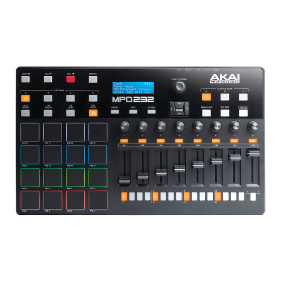
Pads
Knobs
Faders
Buttons
Display
Connections
Power
Dimensions
(width x depth x height)
Weight
SPECIFICATIONS
16 velocity- and pressure-sensitive pads, RGB-backlit
4 banks accessible via Pad Bank buttons
8 360° assignable potentiometers
3 banks accessible via Control Bank buttons
1 360° encoder for display navigation and selection via push
8 45mm assignable faders
3 banks accessible via Control Bank buttons
8 assignable switches, amber-backlit
17 dedicated function buttons, amber-backlit
3 transport buttons
4 directional cursor buttons for display navigation
16 step buttons, red-green-backlit
1 step sequencer bank button with 2 red LEDs
1 step sequencer record button, red-backlit
20 x 4 characters, monochrome backlit with adjustable contrast
1 USB port
1 power input (power adapter sold separately)
1 1/8" MIDI input (1/8"-MIDI adapter included)
1 1/8" MIDI output (1/8"-MIDI adapter included)
1 Kensington lock slot
via computer USB bus or USB charger (sold separately)
via power adapter (sold separately): 6V DC, 1A, center-positive
16.6" x 10.0" x 1.9"
42.2 cm x 25.4 cm x 4.8 cm
4.2 lbs.
1.9 kg
MODEL:MPD232
Advertisement
Table of Contents

Related Manuals for Akai MPD232


Summary of Contents for Akai MPD232
- Page 1 SERVICE MANUAL MODEL:MPD232 SPECIFICATIONS 16 velocity- and pressure-sensitive pads, RGB-backlit Pads 4 banks accessible via Pad Bank buttons 8 360° assignable potentiometers Knobs 3 banks accessible via Control Bank buttons 1 360° encoder for display navigation and selection via push...
-
Page 2: Disassembly Procedures
T e c h n i c a l S p e c i f i c a t i o n T e c h n i c a l S p e c i f i c a t i o n T e c h n i c a l S p e c i f i c a t i o n T e c h n i c a l S p e c i f i c a t i o n DISASSEMBLY PROCEDURES... - Page 3 3.DISASSEMBLE THE CONTROL PCB ASS’Y .(Fig.3) (A) REMOVE 6 SCREWS FROM THE CONTROL PCB ASS’Y. (B) REMOVE 2 CABLES. (Fig.3) 4.DISASSEMBLE THE MAIN PCB ASS’Y .(Fig.4) (A) REMOVE 9 KNOBS, 8 FADERS. (B) REMOVE 9 NUTS AND 9 WASHERS. (C) REMOVE 12 SCREWS FROM THE MAIN PCB ASS’Y. (Fig.4)
-
Page 4: Wiring Diagram
WIRING DIAGRAM (US/AUS) SEQUENCE NO OF EXPLODE DIAGRAM WILL BE MARKED ON REF. COLUMN OF BOM LIST... -
Page 5: Packing Diagram
PACKING DIAGRAM (US) - Page 6 PACKING DIAGRAM (AUS)
-
Page 7: Explode Diagram
EXPLODE DIAGRAM (US/AUS) - Page 8 AD33AKA01 DESCRIPTION LEVEL AD33AKA01 MPD232 100~240AC USA BASJ5012B PU Stand CA030000503 TRS Cable 50mm 3.5φ/MIDI Type Black CA040218002 Usb Cable 1.8M A/B Black FFC1410001002 FFC 14P Pitch:1.0mm,Length:100mm FFC1610001501 FFC 16Pin Pitch:1.0mm Length:150mm FFC5005001001 FFC 50P 0.5MM 100MM LAC22AKA387 Sticker Barcode S/N AD33...
- Page 9 SC0308PBNI Screw SC0310RBBI Screw M3X10 PPB Tapping SC2608PBNI Screw M2.6*8 PPN Tapping TWPC14A01601 FSR PCB Assembly AL2-49-0070 Diode BAV70 D213~220 AL2-71-1324 IC LMV324 SOP-14 U305 AL4-21-5000-R FCN Down Touch ZIF SMD Pitch:0.5mm 50P J301 (Reel) CS103K5003X7R CCAP SMD 0.01uF/50V 10% 0603 X7R C382,384,386,388 CS104K5003X7R CCAP SMD 0.1uF/50V 10% 0603 X7R...
- Page 10 CS105K1603X7R CCAP SMD 1uF/16V 10% 0603 X7R C9,57,177,178 CS106K0605X5R CCAP SMD 10uF/6.3V 10% 0805 X5R C3,19,20,22,50,78,80,108,147,150,176 CS106K1606X5R CCAP SMD 10UF/16V 10% 1206 X5R C48,73 CS180J5003NPO CCAP SMD 18pF/50V 5% 0603 NPO C25,49 DIBAW56 Switch Diode BAW56 SOT-23 D1,4 DIPHLTV-356T-B optical coupler Diode LTV-356T-B SEN2 DISDMBRA340T3G Shottky diode DISDMBRA340T3G SMD 3A 40V...
- Page 11 RS080608F05 RES 806 1% SMD 0805 R135 RS100K08F05 RES 100K 1% SMD 0805 R48,69,155 RS1K9608F05 RES 1.96K 1% SMD 0805 RS220K08F05 RES 220K 1% SMD 0805 R68,124,125 RS2K1508F05 RES 2.15K 1% SMD 0805 R166 RS2K4308F05 RES 2.43K 1% SMD 0805 RS4K7508F05 RES 4.75K 1% SMD 0805 R243...
-
Page 12: Hardware Setup
This document is intended to describe the operation of the ADT1 Manufacturing Test application for the Production Testing of MPD232. Terms MPD232: A USB Pad Controller. Also known as AD33. ADT1: A Manufacturing Test application that runs on Windows computers. Hardware setup ADT1 expects the following connections to be made: 1. -
Page 13: Software Setup
The ports that need to be selected depend on the sub-tests that are being performed for that product. In addition to the main USB-MIDI port, the Manufacturing test for MPD232 requires that a port be selected for the MIDI loopback test. -
Page 14: User Interface
Midi Loopback port selection The next Chooser window will allow the Tester to select the port used for the MIDI loopback test. Select the correct port and click “OK”. This selection should only need to be done once when the program is first run. User Interface The Main Test screen has a representation of the Device Under Test. -
Page 15: Version Number
(i.e. every subtest button is green). Serial Number When a test starts, the Serial Number of the MPD232 will be read and displayed in the bottom left corner. The Serial Number will also be read from the MPD232 and displayed after Serialisation has completed. - Page 16 This test requires a MIDI cable to be connected between the MIDI IN and MIDI OUT connectors on the rear panel. Test messages are sent to the MPD232 for transmission from the MIDI OUT connector on the rear panel. The ADT1 Manufacturing Test app looks for these messages to be received back on the MIDI IN connector.
-
Page 17: Led Tests
In each case, the ADT1 Manufacturing Test app will send a message to flash LEDs on the MPD232. The User interface will indicate which LEDs are flashing and what colour they should be. The Tester should indicate whether the test passed by pressing the UI controls indicated by the “bubble”... -
Page 18: Button Test
User Interface and, where possible, it will send a message to light the LED that is associated with the button on the MPD232. The buttons can be pressed in any order, but if ADT1 detects two button events at exactly... -
Page 19: Fader Test
Fader Test This test requires that the Test operate the indicated Faders to their minimum and then maximum limits. When the Minimum has been reached, the graphic symbol on the User Interface will change. - Page 20 User interface and send a message to the MPD232 to light the associated Pad LED. When the ADT1 Manufacturing Test application detects maximum pad pressure, it will change the graphic symbol to green and send a message to the MPD232 to switch off the associated Pad LED.
- Page 21 Rotary Encoder test The Tester needs to turn the encoder first clockwise and the anti-clockwise as indicated by the ADT1 Manufacturing Test application. ADT1 will check that all possible values are received from the knob control. The progress of the test is indicated by the graphics on the control. Graphics ADT1 Tester...
- Page 22 Tester should move to next knob clockwise values. This knob has passed test. LCD Test In this test, the ADT1 Manufacturing Test application will send messages to the MPD232 to set all the segments on the LCD display first on and then off.
- Page 23 The Tester can type the Serial Number, followed by Carriage Return, but it is preferred that a USB Barcode Reader is used to scan the serial number barcode on the MPD232. When the Serialisation has completed successfully, the display will update.
- Page 24 Test Complete - Next MPD232 When a test of a MPD232 is complete, either successful or unsuccessful, it should be possible to just disconnect that MPD232 and connect the next one. It would not normally be necessary to reselect the ports as long as the corresponding test on the previous...
- Page 25 SW_SEQ REC LED_PAD BANK D LED_SEQ REC SW_PAD BANK D LED_FULL LEVEL SW_FULL LEVEL SW_RECORD SW_16 LEVELS LED_PAD BANK C LED_16 LEVELS SW_PAD BANK C VLED SW_TAP TEMPO LED_TAP TEMPO SW_PLAY SW_NOTE REPEAT SW_STOP LED_NOTE REPEAT LED_PAD BANK A SW_PAD BANK A LED_PAD BANK B SW_PAD BANK B VLED...
- Page 26 PAD 16 PAD 15 PAD 14 PAD 13 PAD 12 PAD 11 PAD 10 PAD 9 PAD 8 PAD 7 PAD 6 PAD 5 PAD 4 PAD 3 PAD 2 PAD 1...
- Page 27 1000pF 1000pF STM32 JTAG 1000pF 1000pF 1000pF 1000pF 1000pF 1000pF VDDA VSSA VBAT R123A R123B R119 R123C R123D...
- Page 28 VDP_SRC = 0.6V ON/OFF...
- Page 29 0.1uF 0.1uF 0.1uF 0.1uF DNS_0.1uF C1024 DNS_0.1uF C1022 DNS_0.1uF C1020 DNS_0.1uF C1018 0.1uF 0.1uF 0.1uF 0.1uF 0.1uF C143 0.1uF C141 0.1uF C139 0.1uF C137 DNS_0.1uF C1135 DNS_0.1uF C1134 DNS_0.1uF C1136 DNS_0.1uF C1133 0.1uF C144 0.1uF C142 0.1uF C140 0.1uF C138 0.1uF 0.1uF 0.1uF...
- Page 32 R215 R189 R197 R210 R214 R188 R196 R209 R213 R187 R195 R203 R212 R186 R194 R202 R211 R185 R193 R201 R122 R184 R192 R200 R183 R191 R199 R182 R190 R198 R 90 R 89 R 88 R 87 R 86 R 85 R 84 R 83...
- Page 34 VLED SW_PAD BANK B LED_PAD BANK B SW_PAD BANK A LED_PAD BANK A LED_NOTE REPEAT SW_STOP SW_NOTE REPEAT SW_PLAY LED_TAP TEMPO SW_TAP TEMPO VLED SW_PAD BANK C LED_16 LEVELS LED_PAD BANK C SW_16 LEVELS SW_RECORD SW_F ULL LEVEL LED_FULL LEVEL SW_PAD BANK D LED_SEQ REC LED_PAD BANK D...
Need help?
Do you have a question about the MPD232 and is the answer not in the manual?
Questions and answers