Sony HCR-S7AV Service Manual

Sony HCR-S7AV Service Manual

Mini hifi component system
Table of Contents

Advertisement

Quick Links

SERVICE MANUAL
Ver 1.0 2001.04
• MHC-S7AV is composed of following models.
As for the service manual, it is issued for each component model, then, please refer to it.
COMPONENT MODEL NAME FOR MHC-S7AV.
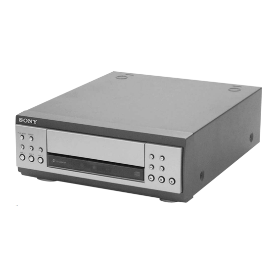
AMPLIFIER
CD PLAYER
TAPE PLAYER
FM STEREO, FM/AM SUPERHETERDYNE TUNER
FRONT SPEAKER
REAR SPEAKER
CENTER SPEAKER
HCR-S7AV is composed of TA-S7AV, CDP-S3, TC-S3, ST-S5, SS-RS270 and SS-CT270.
SPECIFICATIONS
Power requirements
European model:
230 V AC, 50/60 Hz
Australian model:
230 – 240 V AC, 50/60 Hz
Mexican model:
120 V AC, 60 Hz
Korean model:
220 V AC, 60 Hz
Other models:
120 V, 220 V or 230 – 240 V AC, 50/60 Hz
Adjustable with voltage selector
Power consumption
European model:
300 watts
0.6 watts (during Power Saving Mode)
Other models:
300 watts
Dimensions (w/h/d)
Approx. 280 × 128 × 350 mm
TA-S7AV:
Approx. 280 × 108 × 340 mm
ST-S5:
Approx. 280 × 108 × 330 mm
CDP-S3:
Approx. 280 × 128 × 330 mm
TC-S3:
Mass
TA-S7AV:
Approx. 7.7 kg
ST-S5:
Approx. 2.1 kg
CDP-S3:
Approx. 2.7 kg
TC-S3:
Approx. 2.4 kg
Supplied accessories:
AM loop antenna (1)
FM lead antenna (1)
Remote commander (1)
Batteries (2)
Speaker cords (5)
Optical cable (1)
Center and rear speaker pads (12)
Design and specifications are subject to change without notice.
Sony Corporation
9-873-830-11
2001D0500-1
Audio Entertainment Group
C 2001.4
General Engineering Dept.
MHC-S7AV
•Abbreviation
AUS : Australian model
MHC-S7AV
KR
TA-S7AV
MX
CDP-S3
TC-S3
ST-S5
SS-S9
SS-RS270
SS-CT270
PARTS LIST
Part No.
Description
ACCESSORIES & PACKING MATERIALS
********************************
1-476-530-11 COMMANDER, STANDARD (RM-SR370AV)
1-501-374-11 ANTENNA, LOOP
1-501-659-71 ANTENNA (FM) (AUS, MX)
1-501-721-11 ANTENNA (LOOP)
1-501-804-11 ANTENNA (FM) (AEP, UK, KR)
1-574-264-11 CORD, LIGHT PLUG (OPTICAL)
1-769-306-11 CORD, SPEAKER (1.5m) (for SS-S9)
1-769-433-11 CORD, SPEAKER (10m) (for SS-RS270)
1-769-433-21 CORD, SPEAKER (2.5m) (for SS-CT270)
4-210-254-01 CUSHION (FOOT) (for SS-CT270/RS270)
4-233-737-11 MANUAL, INSTRUCTION (ENGLISH) (AEP, UK, AUS)
4-233-737-21 MANUAL, INSTRUCTION (FRENCH) (AEP)
4-233-737-31 MANUAL, INSTRUCTION (SPANISH) (AEP, MX)
4-233-737-41 MANUAL, INSTRUCTION (GERMAN, DUTCH, ITALIAN)
4-233-737-51 MANUAL, INSTRUCTION (SWEDISH) (AEP)
4-233-737-81 MANUAL, INSTRUCTION (KOREAN) (KR)
4-233-745-11 MANUAL, INSTRUCTION (DANISH, FINNISH) (AEP)
4-233-745-21 MANUAL, INSTRUCTION (PORTUGUESE) (AEP)
4-233-745-31 MANUAL, INSTRUCTION (RUSSIAN) (AEP)
4-233-745-41 MANUAL, INSTRUCTION (GREEK) (AEP)
4-233-745-51 MANUAL, INSTRUCTION (HUNGARIAN, CZECH) (AEP)
4-233-745-61 MANUAL, INSTRUCTION (TURKISH) (AEP)
4-233-745-71 MANUAL, INSTRUCTION (SLOVAKIAN) (AEP)
4-981-643-21 COVER, BATTERY (for RM-SR370AV)
MINI HiFi COMPONENT SYSTEM
HCR-S7AV
AEP Model
UK Model
E Model
Australian Model
: Korea model
: Mexican model
Remark
(AEP)

Advertisement

Table of Contents
loading

Summary of Contents for Sony HCR-S7AV

  • Page 1 FM STEREO, FM/AM SUPERHETERDYNE TUNER ST-S5 FRONT SPEAKER SS-S9 REAR SPEAKER SS-RS270 CENTER SPEAKER SS-CT270 HCR-S7AV is composed of TA-S7AV, CDP-S3, TC-S3, ST-S5, SS-RS270 and SS-CT270. SPECIFICATIONS PARTS LIST Power requirements Part No. Description Remark European model: 230 V AC, 50/60 Hz ACCESSORIES &...
  • Page 2 MHC-S7AV REVISION HISTORY Clicking the version allows you to jump to the revised page. Also, clicking the version at the upper right on the revised page allows you to jump to the next revised page. Ver. Date Description of Revision 2001.04...
  • Page 3 Dimensions (w/h/d) Approx. 280 x 108 x 330 mm Mass Approx. 2.7 kg Design and specifications are subject to change without notice. COMPACT DISC PLAYER Sony Corporation 9-873-831-11 2001D0500-1 Home Audio Company C 2001.4 Shinagawa Tec Service Manual Production Group...
  • Page 4 LINE WITH MARK 0 ON THE SCHEMATIC DIAGRAMS AND IN THE PARTS LIST ARE CRITICAL TO SAFE OPERATION. REPLACE THESE COMPONENTS WITH SONY PARTS WHOSE PART NUMBERS APPEAR AS SHOWN IN THIS MANUAL OR IN SUPPLEMENTS PUB- LISHED BY SONY.
  • Page 5: Table Of Contents

    CDP-S3 TABLE OF CONTENTS SERVICING NOTES ..........4 GENERAL ..............5 DISASSEMBLY 3-1. Disassembly Flow ............6 3-2. Cover ................7 3-3. CD Mechanism Deck (CDM63B-30BD60) ....7 3-4. MAIN Board ..............8 3-5. Front Panel Section ............8 3-6. PANEL (L) Board, PANEL (R) Board ......9 3-7.
  • Page 6: Servicing Notes

    CDP-S3 SECTION 1 SERVICING NOTES This set is a component of the MHC-S7AV or MHC-S3. CD-TEXT TEST DISC The MHC-S7AV or MHC-S3 system configuration is as shown below, and therefore it does not operate normally unless all four This unit is able to display the test data (character information) components are connected.
  • Page 7: General

    CDP-S3 SECTION 2 This section is extracted from instruction manual. GENERAL Parts Identification The items are arranged in alphabetical order. Refer to the pages indicated in parentheses ( ) for details. Main unit Remote Control wj wkwl e; ea 1 2 3 CD H es (14, 15) CHECK 5 (15) CLEAR 6 (15)
  • Page 8: Disassembly

    CDP-S3 SECTION 3 DISASSEMBLY • This set can be disassembled in the order shown below. 3-1. DISASSEMBLY FLOW 3-2. COVER (Page 7) 3-3. CD MECHANISM DECK 3-5. FRONT PANEL SECTION 3-4. MAIN BOARD (CDM63B-30BD60) (Page 8) (Page 8) (Page 7) 3-6.
  • Page 9: Cover

    CDP-S3 Note: Follow the disassembly procedure in the numerical order given. 3-2. COVER 2 screw 3 cover (BVTT3 × 6) 1 two screws (case 3 TP2) 1 two screws (case 3 TP2) 3-3. CD MECHANISM DECK (CDM63B-30BD60) 4 CD mechanism deck (CDM63B-30BD60) 2 connector (CN701)
  • Page 10: Main Board

    CDP-S3 3-4. MAIN BOARD 2 two connectors (CN101, 102) 1 wire (flat type) (21 core) (CN301) 5 MAIN board 2 connector (CN401) 3 screw (BVTP3 × 8) 3 two screws (BVTP3 × 8) 4 lug 3 screw (BVTP3 × 8) 2 connector (CN701) 3-5.
  • Page 11: Panel (L) Board, Panel (R) Board

    CDP-S3 3-6. PANEL (L) BOARD, PANEL (R) BOARD 4 four screws (BVTP2.6 × 8) 6 PANEL (R) board 5 two claws 1 five screws (BVTP2.6 × 8) 3 PANEL (L) board 2 two claws 3-7. LID (CD) 2 bracket (LID) assy 1 screw (BVTP2.6 ×...
  • Page 12: Test Mode

    CDP-S3 SECTION 4 TEST MODE Note: Use flowing buttons in the test mode. [CD Service Mode] no mark : Button of CD unit (CDP-S3) • This mode can run the CD sled motor optionally. Use this mode, : Button of amplifier unit (TA-S7AV or TA-S3) for instance, when cleaning the optical pick-up.
  • Page 13: Electrical Adjustments

    CDP-S3 SECTION 5 ELECTRICAL ADJUSTMENTS Note : E-F Balance (1 Track jump) Check 1. CD Block is basically designed to operate without adjustment. Therefore, check each item in order given. oscilloscope BD board 2. Use LUV-P01 (4-999-032-01) unless otherwise indicated. 3.
  • Page 14: Diagrams

    CDP-S3 SECTION 6 DIAGRAMS 6-1. NOTE FOR PRINTED WIRING BOARDS AND SCHEMATIC DIAGRAMS (In addition to this, the necessary note is printed in each block) Note on Printed Wiring Boards: Note on Schematic Diagram: • All capacitors are in µF unless otherwise noted. pF: µµF •...
  • Page 15 CDP-S3 • Circuit Boards Location PANEL (R) board MAIN board PANEL (L) board TRAY SENSOR board IN OUT SW board DRIVER board BD board MOTOR board DISC SENSOR board...
  • Page 16: Printed Wiring Board - Bd Section

    CDP-S3 6-2. PRINTED WIRING BOARD – BD Section – • See page 13 for Circuit Boards Location. (Page 18) MAIN BOARD CN301 M102 (SLED) M101 (SPINDLE) (RFDC) (FEO) (DVC) (RFAC) (FEI) • Semiconductor Location Ref. No. Location D101 IC101 IC102 IC103 There are a few cases that the part printed on Q101...
  • Page 17: Schematic Diagram -Bd Section

    CDP-S3 6-3. SCHEMATIC DIAGRAM – BD Section – • • See page 22 for Waveforms. See page 22 for IC Block Diagrams. (RFAC) TP (DVC) (RFDC) (TEO) IC B/D IC B/D (FEO) IC B/D MAIN BOARD CN301 (Page 19) • Voltages and waveforms are dc with respect to ground Note: The components identified by mark 0 or dotted line under no-signal conditions.
  • Page 18 CDP-S3 6-4. PRINTED WIRING BOARDS – CD CHANGER Section – • See page 13 for Circuit Boards Location. MAIN BOARD NO202 (Page 18) There are a few cases that the part isn't mounted in model is printed on diagrams.
  • Page 19 CDP-S3 6-5. SCHEMATIC DIAGRAM – CD CHANGER Section – • See page 22 for IC Block Diagram. IC731 SUB TRAY1 HEIGHT SENSOR IC732 SUB TRAY2 HEIGHT SENSOR IC733 SUB TRAY3 HEIGHT SENSOR MAIN BOARD NO202 (Page 19) IC751 DISC IN DETECT •...
  • Page 20 CDP-S3 6-6. PRINTED WIRING BOARD – MAIN Section – • See page 13 for Circuit Boards Location. (Page 14) (Page 16) SYSTEM CONTROL 3 BD BOARD DRIVER BOARD TO ST-S3/S5 CN101 CN701 MAIN BOARD (CHASSIS) SYSTEM CONTROL 5 TO TC-S3 IC401 OPTICAL OUT TO ST-S3/S5...
  • Page 21: Schematic Diagram - Main Section

    CDP-S3 6-7. SCHEMATIC DIAGRAM – MAIN Section – • See page 22 for Waveform. OPTICAL OUT TO ST-S3/S5 CLP102 C122 CN301 IC102 0.022 TOTX140 PWM3 CD301 C103 C102 C101 C125 OPTICAL (CHASSIS) PWM2 C301 0.47 CD302 D502 D501 TRANSCEIVER 11ES2 11ES2 PWM1 C302...
  • Page 22: Printed Wiring Boards - Panel Section

    CDP-S3 6-8. PRINTED WIRING BOARDS – PANEL Section – • See page 13 for Circuit Boards Location. (Page 18) PANEL (R) BOARD REPEAT PLAY MODE > (DISC 3) PANEL (L) BOARD (DISC 2) (DISC 1) DISC 3 DISC 2 DISC 1 1-680-995- (21) 1-680-996-...
  • Page 23: Schematic Diagram - Panel Section

    CDP-S3 6-9. SCHEMATIC DIAGRAM – PANEL Section – R707 R706 R705 R704 R703 R702 R701 R700 1.8k 1.2k CN701 S708 S707 S706 S705 S704 S703 S702 S701 PLAY MODE REPEAT DISC 1 DISC 2 DISC 3 (DISC 3) (DISC 2) (DISC 1) R716 R715...
  • Page 24 CDP-S3 • Waveforms • IC Block Diagrams – BD Board – – MAIN Board – – BD Board – qa IC401 qd (X-OUT) 1 IC101 ta (RFAC) (CD Play mode) IC101 CXD3017Q 1.1 Vp-p 2.6 Vp-p ERROR DIGITAL CORRECTOR DIGITAL ASYMMETRY CORRECTOR OPERATIONAL...
  • Page 25 CDP-S3 – DRIVER Board – IC103 CXA2581N-T4 IC701 BA6956AN RW/ROM DC OFST RFDCI – – RFDCO CONTROL LOGIC – RW/ROM VOFST APC AMP EQ ON/OFF RFAC EQ IN RW/ROM RFAC AC SUM SUMMING VOFST – – RW/ROM TE BAL RW/ROM –...
  • Page 26: Ic Pin Function Description

    CDP-S3 6-10. IC PIN FUNCTION DESCRIPTION • MAIN BOARD IC401 M30620MAA-B31FP (SYSTEM CONTROLLER) Pin No. Pin Name Description 1 to 7 — — Not used (open) External data bus line byte selection signal input “L”: 16 bits, “H”: 8 bits BYTE Not used (fixed at “L”) CNVSS...
  • Page 27 CDP-S3 Pin No. Pin Name Description Detection input from the disc tray 3 height sensor (IC733) T-SENS3 “H”: disc tray 3 position is chucking position — — Not used (fixed at “H”) DISC-SENS Detection input from the disc in detect sensor (IC751) Deck-B trigger plunger drive signal output to the tape deck unit (TC-S3) B-TRIG “H”: trigger plunger on...
  • Page 28: Exploded Views

    CDP-S3 SECTION 7 EXPLODED VIEWS NOTE: • -XX and -X mean standardized parts, so they • Items marked “*” are not stocked since they The components identified by mark 0 or dotted line with mark may have some difference from the original are seldom required for routine service.
  • Page 29: Cd Mechanism Deck Section-1 (Cdm63B-30Bd60)

    CDP-S3 7-2. CD MECHANISM DECK SECTION-1 (CDM63B-30BD60) not supplied not supplied not supplied not supplied supplied not supplied not supplied not supplied not supplied not supplied not supplied Ref. No. Part No. Description Remark Ref. No. Part No. Description Remark 4-218-253-01 SCREW (M2.6), +BTTP 4-228-964-01 SLIDER (STOCKER.
  • Page 30: Cd Mechanism Deck Section-2 (Cdm63B-30Bd60)

    CDP-S3 7-3. CD MECHANISM DECK SECTION-2 (CDM63B-30BD60) BU-30BD60 not supplied not supplied not supplied M721 Ref. No. Part No. Description Remark Ref. No. Part No. Description Remark 4-985-672-01 SCREW (+PTPWH M2.6), FLOATING 4-228-968-01 BELT 4-229-002-02 GEAR (SLIDER) 4-228-998-01 GEAR (DETECTION) 4-218-254-21 SCREW (M2.6), +PTPWH 4-228-976-01 SLIDER (BU.
  • Page 31: Base Unit Section (Bu-30Bd60)

    CDP-S3 7-4. BASE UNIT SECTION (BU-30BD60) not supplied not supplied not supplied The components identified by mark 0 or dotted line with mark 0 are critical for safety. Replace only with part number specified. Ref. No. Part No. Description Remark Ref.
  • Page 32: Electrical Parts List

    CDP-S3 SECTION 8 ELECTRICAL PARTS LIST NOTE: • Due to standardization, replacements in the • Items marked “*” are not stocked since they The components identified by mark 0 or dotted line with mark parts list may be different from the parts speci- are seldom required for routine service.
  • Page 33 CDP-S3 DISC SENSOR DRIVER IN OUT SW MAIN Ref. No. Part No. Description Remark Ref. No. Part No. Description Remark Q102 8-729-920-85 TRANSISTOR 2SD1664-T100-QR 1-678-463-11 DISC SENSOR BOARD ****************** < RESISTOR > < PHOTO REFLECTOR > R101 1-216-049-11 RES-CHIP 1/10W R102 1-216-097-11 RES-CHIP 100K...
  • Page 34 CDP-S3 MAIN Ref. No. Part No. Description Remark Ref. No. Part No. Description Remark D513 8-719-024-99 DIODE 11ES2-NTA2B C122 1-161-494-00 CERAMIC 0.022uF D514 8-719-024-99 DIODE 11ES2-NTA2B C124 1-164-159-11 CERAMIC 0.1uF C125 1-126-923-11 ELECT 220uF D515 8-719-024-99 DIODE 11ES2-NTA2B C251 1-161-494-00 CERAMIC 0.022uF C255 1-161-494-00 CERAMIC...
  • Page 35 CDP-S3 MAIN MOTOR PANEL (L) PANEL (R) TRAY SENSOR Ref. No. Part No. Description Remark Ref. No. Part No. Description Remark R435 1-247-807-31 CARBON 1/4W 1-680-995-11 PANEL (L) BOARD R436 1-247-807-31 CARBON 1/4W *************** R437 1-247-807-31 CARBON 1/4W < LED > R438 1-247-807-31 CARBON 1/4W...
  • Page 36 CDP-S3 TRAY SENSOR Ref. No. Part No. Description Remark Ref. No. Part No. Description Remark < PHOTO SENSOR > IC731 8-749-081-01 PHOTO SENSOR DG-264 IC732 8-749-081-01 PHOTO SENSOR DG-264 IC733 8-749-081-01 PHOTO SENSOR DG-264 < RESISTOR > R731 1-247-876-11 CARBON 1/4W R732 1-249-408-11 CARBON...
  • Page 37 CDP-S3 MEMO...
  • Page 38 CDP-S3 REVISION HISTORY Clicking the version allows you to jump to the revised page. Also, clicking the version at the upper right on the revised page allows you to jump to the next revised page. Ver. Date Description of Revision 2001.04...
  • Page 39 UK Model E Model Australian Model Photo: SS-S3 • SS-S3 are speaker system in MHC-S3. • SS-S9 are speaker system in MHC-S7AV, MHC-SV7AV. SPECIFICATIONS SPEAKER SYSTEM Sony Corporation 9-873-835-12 2002G0500-1 Home Audio Company C 2002.07 Published by Sony Engineering Corporation...
  • Page 40 SS-S3/S9 Ver 1.1 DISASSEMBLY Note: Follow the disassembly procedure in the numerical order given. FRONT PANEL SECTION tapping screw 3 four tapping screws (3.5 × 14) catcher 2 four catchers 1 grille frame assy To remove the front panel section, stick a hexagon wrench into the hole A, B, C and D hole B and pull up with pliers as shown in the Fig.
  • Page 41 SS-S3/S9 EXPLODED VIEWS AND PARTS LIST NOTE: • Items marked “*” are not stocked since they • The mechanical parts with no reference num- • Color Indication of Appearance Parts are seldom required for routine service. Some ber in the exploded views are not supplied. Example: delay should be anticipated when ordering KNOB, BALANCE (WHITE) .
  • Page 42 SS-S3/S9 REVISION HISTORY Clicking the version allows you to jump to the revised page. Also, clicking the version at the upper right on the revised page allows you to jump to the next revised page. Ver. Date Description of Revision 2001.04 2002.07 Change of DISASSEMBLY of Front Panel Section.
  • Page 43 1 mV, 75 + 75 watts (Except for impedance 10 kilohms (8 ohms at 1 kHz, 10% European model) THD) (phone jack) AV AMPLIFIER Sony Corporation 9-873-836-11 2001D0500-1 Home Audio Company C 2001.4 Shinagawa Tec Service Manual Production Group...
  • Page 44 LINE WITH MARK 0 ON THE SCHEMATIC DIAGRAMS AND IN THE PARTS LIST ARE CRITICAL TO SAFE OPERATION. REPLACE THESE COMPONENTS WITH SONY PARTS WHOSE PART NUMBERS APPEAR AS SHOWN IN THIS MANUAL OR IN SUPPLEMENTS PUB- LISHED BY SONY.
  • Page 45: Servicing Notes

    TA-S7AV SECTION 1 SERVICING NOTES This set is a component of the MHC-S7AV. MODEL IDENTIFICATION The MHC-S7AV system configuration is as shown below, and therefore it does not operate normally unless all four components – Back Panel – are connected. In performing the repair, connect all components with the system cables.
  • Page 46: General

    TA-S7AV SECTION 2 This section is extracted from instruction manual. GENERAL Parts Identification The items are arranged in alphabetical order. Refer to the pages indicated in parentheses ( ) for details. Main unit Remote Control 1 2 3 CD H es (14, 15) CHECK 5 (15) CLEAR 6 (15) CLOCK/TIMER SELECT qj...
  • Page 47: Disassembly

    TA-S7AV SECTION 3 DISASSEMBLY • This set can be disassembled in the order shown below. 3-1. DISASSEMBLY FLOW Note 1: The process described in can be performed in any order. Note 2: Without completing the process described in , the next process can not be performed. 3-2.
  • Page 48: Cover

    TA-S7AV Note: Follow the disassembly procedure in the numerical order given. 3-2. COVER 1 three screws 4 Remove the cover (BVTT3 × 6) in the direction of arrow A . 2 two screws (case 3 TP2) 2 two screws (case 3 TP2) 3-3.
  • Page 49: Back Panel (Av) Section

    TA-S7AV 3-4. BACK PANEL (AV) SECTION 8 back panel (AV) section 5 three screws (BVTP3 × 8) 5 four screws 7 three connectors (BVTP3 × 8) (CN901, 902, 903) 1 screw (BVTP3 × 8) 5 four screws (BVTP3 × 8) 6 connector (CN105) 1 screw...
  • Page 50: Test Mode

    TA-S7AV SECTION 4 TEST MODE Note: Use flowing buttons in the test mode. [GC Test Mode] no mark : Button of amplifier unit (TA-S7AV) Enter the GC Test Mode : Button of tuner unit (ST-S5) Procedure 1: : Button of CD unit (CDP-S3) 1.
  • Page 51 TA-S7AV MEMO...
  • Page 52: Diagrams

    TA-S7AV SECTION 5 DIAGRAMS 5-1. NOTE FOR PRINTED WIRING BOARDS AND SCHEMATIC DIAGRAMS Note on Printed Wiring Boards: Note on Schematic Diagram: • All capacitors are in µF unless otherwise noted. pF: µµF • X : parts extracted from the component side. •...
  • Page 53: Printed Wiring Boards - Front Amp Section

    TA-S7AV 5-2. PRINTED WIRING BOARDS – FRONT AMP Section – • See page 10 for Circuit Boards Location. • Semiconductor Location NO102 Ref. No. Location Ref. No. Location Ref. No. Location Ref. No. Location D911 C911 (Page 18) D801 D970 D996 Q883 D802...
  • Page 54 TA-S7AV 5-3. SCHEMATIC DIAGRAM – FRONT AMP Section (1/2) – (1/2) NO109 SUB-AC SUB-AC RELAY-UNREG STBY RELAY +5.6V REGULATOR D998 DGND (Page 19) IC924 D991 D990 NJM78L05A-T3 11ES2-NTA2 11ES2-NTA2 JOG2-B(FIELD SELECT) TP205 JOG2-B JOG2-A(FIELD SELECT) TP204 JOG2-A D993 D992 C992 11ES2-NTA2 11ES2-NTA2 JOG1-B(FUNCTION)
  • Page 55: Schematic Diagram - Front Amp Section (1/2)

    TA-S7AV 5-4. SCHEMATIC DIAGRAM – FRONT AMP Section (2/2) – (2/2) NO101 (Page 19) TP107 TP106 AC4(HIGH) TP105 AC4(HIGH) TP104 AC3(LOW) TP103 AC3(LOW) (Page 19) TP102 TP101 POWER AMP IC801 EPT901 C987 STK402-120S (CHASSIS) D911 D5SBA20 C911 NO102 100V TP108 C912 R971 (Page 19)
  • Page 56: Ic Pin Function Description

    TA-S7AV 5-5. IC PIN FUNCTION DESCRIPTION 5-6. PRINTED WIRING BOARD – SURROUND AMP Section – • See page 10 for Circuit Boards Location. • MAIN BOARD IC301 PT8300-S (SYSTEM CONTROLLER) Pin No. Pin Name Description — Ground terminal RESET_B Reset signal input terminal Not used SURROUND AMP BOARD Serial data transfer clock signal input from the tuner unit (ST-S5) R1094...
  • Page 57: Schematic Diagram - Surround Amp Section

    TA-S7AV 5-7. SCHEMATIC DIAGRAM – SURROUND AMP Section – POWER AMP R1094 R1093 100k IC1001 STK443-050 Q1092,1093 THERMAL DETECT Q1092 2SC2785 R1092 100k Q1093 2SC2785 CN1003 R1095 THP092 OVERLOAD DETTECT C1001 R1005 R1090 R1001 0.22 D1002 1SS133T R1060 (Page 13) R1010 C1003 100p...
  • Page 58: Printed Wiring Boards - Control Section

    TA-S7AV 5-8. PRINTED WIRING BOARDS – CONTROL Section – • See page 10 for Circuit Boards Location. R724 C781 PANEL BOARD MULTI CHANNEL D781 DECODING D704, S712 NO781 D701, S705 JW521 CINEMA STUDIO R715 NO711 D706 D705 D704 D701 R713 D706, S714 NO710 CINEMA...
  • Page 59: Schematic Diagram - Control Section

    TA-S7AV 5-9. SCHEMATIC DIAGRAM – CONTROL Section – S701 S702 S703 FUNCTION FILE SELECT VOLUME ROTARY ENCODER ROTARY ENCODER ROTARY ENCODER R716 R717 R718 R719 2.2k 2.7k 3.9k 5.6k S723 ENTER C701 C703 0.01 0.01 C702 C704 C705 C706 0.01 0.01 0.01 0.01...
  • Page 60: Printed Wiring Boards - Power Section

    TA-S7AV 5-10. PRINTED WIRING BOARDS – POWER Section – • See page 10 for Circuit Boards Location. (AC IN) SUB TRANS BOARD JW803 Q901 JW804 JW801 JW907 RY901 JW903 FRONT AMP JW805 BOARD R901 R902 JW913 NO109 JW806 (Page 11) D901 LP102 CN901...
  • Page 61: Schematic Diagram - Power Section

    TA-S7AV 5-11. SCHEMATIC DIAGRAM – POWER Section – F931 T8AL 250V T911 POWER (AUS) TRANSFORMER AC1-GND (MAIN) JW921 F932 (AEP,UK,KR) T6.3AL JW922 NO921 CN902 AC2-GND JW923 120/230 120/230 JW913 JW907 (Page 13) F933 CN913 T6.3AL 250V (MX) NEUTRAL NEUTRAL C901 0.01 (Page 13) 250V...
  • Page 62: Exploded Views

    TA-S7AV SECTION 6 EXPLODED VIEWS NOTE: 6-2. FRONT PANEL SECTION • -XX and -X mean standardized parts, so they • Items marked “*” are not stocked since they The components identified by mark 0 or dotted line with mark may have some difference from the original are seldom required for routine service.
  • Page 63: Chassis Section

    TA-S7AV 6-3. CHASSIS SECTION not supplied not supplied T911 not supplied not supplied not supplied not supplied not supplied not supplied The components identified by mark 0 or dotted line with mark 0 are critical for safety. Replace only with part number specified. Ref.
  • Page 64: Electrical Parts List

    TA-S7AV SECTION 7 AC INPUT AC OUTPUT ELECTRICAL PARTS LIST FRONT AMP NOTE: • Due to standardization, replacements in the • Items marked “*” are not stocked since they The components identified by mark 0 or dotted line with mark parts list may be different from the parts speci- are seldom required for routine service.
  • Page 65 TA-S7AV FRONT AMP Ref. No. Part No. Description Remark Ref. No. Part No. Description Remark C926 1-126-382-11 ELECT 100uF D990 8-719-024-99 DIODE 11ES2-NTA2B C927 1-104-665-11 ELECT 100uF D991 8-719-024-99 DIODE 11ES2-NTA2B C941 1-164-159-11 CERAMIC 0.1uF D992 8-719-024-99 DIODE 11ES2-NTA2B C951 1-135-516-11 ELECT 3300uF D993...
  • Page 66 TA-S7AV FRONT AMP PANEL Ref. No. Part No. Description Remark Ref. No. Part No. Description Remark R811 1-260-076-11 CARBON 1/2W R905 1-249-421-11 CARBON 2.2K 1/4W (AEP, UK) R906 1-249-417-11 CARBON 1/4W R812 1-260-076-11 CARBON 1/2W R907 1-249-421-11 CARBON 2.2K 1/4W (AEP, UK) R908 1-249-421-11 CARBON...
  • Page 67 TA-S7AV PANEL Ref. No. Part No. Description Remark Ref. No. Part No. Description Remark C704 1-162-306-11 CERAMIC 0.01uF < JACK > C705 1-162-306-11 CERAMIC 0.01uF J702 1-691-293-21 JACK (MIC) (KR, MX, AUS) C706 1-162-306-11 CERAMIC 0.01uF J703 1-691-293-21 JACK (PHONES) C710 1-162-294-31 CERAMIC 0.001uF...
  • Page 68 TA-S7AV PANEL RELAY SUB TRANS SURROUND AMP Ref. No. Part No. Description Remark Ref. No. Part No. Description Remark S702 1-473-534-11 ENCODER, ROTARY (FILE SELECT) A-2007-897-A SURROUND AMP BOARD, COMPLETE S703 1-473-392-11 ENCODER, ROTARY (VOLUME) (KR, MX, AUS) S705 1-771-410-21 SWITCH, TACTILE (I/1) A-4476-217-A SURROUND AMP BOARD, COMPLETE S710 1-771-410-21 SWITCH, TACTILE (SUR)
  • Page 69 TA-S7AV SURROUND AMP Ref. No. Part No. Description Remark Ref. No. Part No. Description Remark R1003 1-249-415-11 CARBON 1/4W MISCELLANEOUS R1004 1-249-438-11 CARBON 1/4W ************** 0 R1005 1-233-352-41 ENCAPSULATED COMPONENT 0.22 1-773-178-11 WIRE (FLAT TYPE) (23 CORE) (AEP, UK) R1006 1-249-417-11 CARBON 1/4W 1-773-210-11 WIRE (FLAT TYPE) (25 CORE) (KR, MX, AUS)
  • Page 70 TA-S7AV REVISION HISTORY Clicking the version allows you to jump to the revised page. Also, clicking the version at the upper right on the revised page allows you to jump to the next revised page. Ver. Date Description of Revision 2001.04...
  • Page 71 8 ohms Dimensions (w/h/d) Approx. 225 x 95 x 100 mm Mass Approx. 1.2 kg net Design and specifications are subject to change without notice. SPEAKER SYSTEM Sony Corporation 9-873-860-11 2001C0900-1 Audio Entertainment Group © 2001. 3 General Engineering Dept.
  • Page 72 SS-CT270/RC270/RS270 EXPLODED VIEW AND PARTS LIST NOTE: • The mechanical parts with no reference num- ber in the exploded views are not supplied. • SS-CT270 Ref. No. Part No. Description Remark ––––––– ––––––– ––––––––– –––––– X-4953-893-1 FRAME ASSY, GRILLE 4-978-600-01 SCREW 4-221-063-11 PANEL, FRONT X-4953-852-1 CABINET ASSY 1-537-775-12 TERMINAL BOARD...
  • Page 73 SS-CT270/RC270/RS270 • SS-RS270 Ref. No. Part No. Description Remark ––––––– ––––––– ––––––––– –––––– X-4953-892-1 FRAME ASSY, GRILLE 4-978-600-01 SCREW 4-232-595-01 PANEL, FRONT X-4953-876-1 CABINET ASSY 1-694-516-11 TERMINAL, SPEAKER 4-874-614-01 SCREW (4) (3.5 X 14), TAPPING 4-229-803-11 PACKING 1-529-982-11 SPEAKER (8CM)
  • Page 74 SS-CT270/RC270/RS270 REVISION HISTORY Clicking the version allows you to jump to the revised page. Also, clicking the version at the upper right on the revised page allows you to jump to the next revised page. Ver. Date Description of Revision 2001.03...
  • Page 75 Dimensions (w/h/d) Approx. 280 x 108 x 340 mm Mass Approx. 2.1 kg Design and specifications are subject to change without notice. FM STEREO/FM-AM SUPERHETERODYNE TUNER Sony Corporation 9-873-832-11 2001D0500-1 Home Audio Company C 2001.4 Shinagawa Tec Service Manual Production Group...
  • Page 76 3-1. Disassembly Flow ............6 OPERATION. REPLACE THESE COMPONENTS WITH 3-2. Cover ................7 SONY PARTS WHOSE PART NUMBERS APPEAR AS 3-3. Front Panel Section ............7 SHOWN IN THIS MANUAL OR IN SUPPLEMENTS PUB- 3-4. PANEL Board, SIRCS Board ......... 8 LISHED BY SONY.
  • Page 77: Servicing Notes

    ST-S5 SECTION 1 SERVICING NOTES This set is a component of the MHC-S7AV. • MODEL IDENTIFICATION The MHC-S7AV system configuration is as shown below, and – Rear Panel – therefore it does not operate normally unless all four components are connected. In performing the repair, connect all components with the system cables.
  • Page 78: General

    ST-S5 SECTION 2 This section is extracted from instruction manual. GENERAL LOCATION OF CONTROLS – Front Panel – qjqk ql w; CLOCK/TIMER wg (13, 21, 29) DISPLAY qh (13, 16, 18, 29, 35) ENTER w; (17, 18) IR receptor wh PRESET +/–...
  • Page 79: Setting The Time

    ST-S5 Setting the time Remote Control Turn on the system. Press CLOCK/TIMER (or CLOCK/TIMER 1 2 3 SET on the remote). When you set the time for the first time, proceed to step 5. Press O or o repeatedly to select “CLOCK SET”.
  • Page 80: Disassembly

    ST-S5 SECTION 3 DISASSEMBLY • This set can be disassembled in the order shown below. 3-1. DISASSEMBLY FLOW 3-2. COVER (Page 7) 3-3. FRONT PANEL SECTION 3-5. TUNER PACK (FM/AM) 3-7. DSP BOARD (Page 7) (Page 8) (Page 9) 3-4. PANEL BOARD, 3-6.
  • Page 81: Cover

    ST-S5 Note: Follow the disassembly procedure in the numerical order given. 3-2. COVER 3 cover 1 screw (+BVTT3 × 6 (S)) 2 two screws (case 3 TP2) 2 two screws (case 3 TP2) 3-3. FRONT PANEL SECTION 1 wire (flat type) (19 core) (CN502) 3 two claws 4 front panel section...
  • Page 82: Panel Board, Sircs Board

    ST-S5 3-4. PANEL BOARD, SIRCS BOARD 2 two screws (BVTP2.6 × 8) 6 SIRCS board 4 PANEL board 2 four screws (BVTP2.6 × 8) 5 two claws 2 screw (BVTP2.6 × 8) (AEP, UK models) 1 wire (flat type) (19 core) (CN602) 3 two claws 3-5.
  • Page 83: Main Board

    ST-S5 3-6. MAIN BOARD 1 wire (flat type) (23 core) (CN508) 2 five connectors (CN510, 5031, 5032, 5041, 5042) 1 wire (flat type) (21 core) (CN509) 6 MAIN board 4 screw 4 two screws (BVTP3 × 8) (BVTP3 × 8) 1 wire (flat type) (19 core) (CN502) 3 three screws...
  • Page 84: Test Mode

    ST-S5 SECTION 4 TEST MODE [GC Test Mode] Note: Use flowing buttons in the test mode. no mark : Button of tuner unit (ST-S5) Enter the GC Test Mode mode : Button of amplifier unit (TA-S7AV) Procedure 1: : Button of CD unit (CDP-S3) 1.
  • Page 85: Diagrams

    ST-S5 SECTION 5 DIAGRAMS 5-1. NOTE FOR PRINTED WIRING BOARDS AND SCHEMATIC DIAGRAMS • Circuit Boards Location Note on Printed Wiring Board: Note on Schematic Diagram: DSP board • All capacitors are in µF unless otherwise noted. pF: µµF • X : parts extracted from the component side. •...
  • Page 86: Schematic Diagram - Main Board (1/2)

    ST-S5 5-2. SCHEMATIC DIAGRAM – MAIN Board (1/2) – (1/2) CN5031 M(A)-GND EVER+5V D-GND NO901 NO991 C991 D+5V +15V REGULATOR (Page 13) IC991 C992 NJM7815FA CN5041 MIC-SIG MIC-GND (A-GND) FL-OUT FRONT-GND FR-OUT CENTER-OUT CENTER-GND (Page 13) SL-OUT S-GND SR-OUT OPTICAL RECEIVER C955 OPTICAL IN 10000p...
  • Page 87 ST-S5 5-3. SCHEMATIC DIAGRAM – MAIN Board (2/2) – • See page 20 for Waveforms. (2/2) CN506 (AEP,UK) (E,AUS) ST-CLK (AEP,UK) R957 ST-DIN MC D0 ST-DOUT MC D1 COAXIAL ST-CE FM 75Ω A+10V R958 TUNED C962 R959 C961 FM/AM STEREO R964 R961 2.2k...
  • Page 88: Printed Wiring Board - Main Board

    ST-S5 5-4. PRINTED WIRING BOARD – MAIN Board – • See page 11 for Circuit Boards Location. • Semiconductor Location Ref. No. Location ANTENNA D551 (E, AUS) D552 (AEP, UK) 75Ω D901 COAXIAL D902 SYSTEM FM 75Ω D903 CONTROL 1 D904 (TO TA-S7AV) D911...
  • Page 89: Printed Wiring Board - Dsp Board

    ST-S5 5-5. PRINTED WIRING BOARD – DSP Board – • See page 11 for Circuit Boards Location. • Semiconductor Location Ref. No. Location J601 VIDEO D601 (AUDIO) D604 J602 D605 D607 WOOFER D608 IC609 DSP BOARD D609 OPTICAL (CONDUCTOR SIDE) D610 DSP BOARD (COMPONENT SIDE)
  • Page 90 ST-S5 5-6. SCHEMATIC DIAGRAM – DSP Board (1/2) – • See page 20 for Waveforms. • See page 20 for IC Block Diagram. C657 1000p C656 C655 R664 CN602 A+5V FB608 A-GND R680 FB607 DIGITAL 3.3k D+5V FILTER, D/A CONVERTER D-GND Q612 JR621...
  • Page 91 ST-S5 5-7. SCHEMATIC DIAGRAM – DSP Board (2/2) – • See page 20 for Waveforms. • See page 20 for IC Block Diagram. Q603 Q603 2SC1623 REGULATOR R776 (E,AUS) R778 C690 C691 R777 R775 R762 FB606 INPUT SELECT SWITCH, C689 GRAPHIC EQUALIZER CONTROL, ELECTRICAL VOLUME...
  • Page 92: Printed Wiring Boards - Panel Section

    ST-S5 5-8. PRINTED WIRING BOARDS – PANEL Section – • See page 20 for Circuit Boards Location. PANEL BOARD C610 JW24 R603 FL601 JW11 C601 FLUORESCENT C653 C655 C657 C659 C661 C651 INDICATOR C649 TUBE C664 S611 C650 S601 SIRCS C666 STEREO/MONO DISPLAY...
  • Page 93 ST-S5 5-9. SCHEMATIC DIAGRAM – PANEL Section – • See page 20 for Waveform. FL601 FLUORESCENT INDICATOR TUBE C610 (AEP,UK) R616 S612 100k CN602 R627 5.6k DISP/STANDBY KEY S611 D-GND STEREO/ MONO JOG2-B JOG2-A S610 R626 JOG1-B 3.9k TUNER MEMORY JOG1-A VOLA S609...
  • Page 94 ST-S5 • Waveforms • IC Block Diagrams – MAIN Board – – DSP Board – – DSP Board – 1 IC501 qa (XCOUT) 1 IC601 9 (MCLK1), IC604 w; (XMCK), 5 IC601 ws (KFSIO), IC604 qd (CKOUT) IC604 LC89056W-E wa (XOUT) 4.4 Vp-p 2.6 Vp-p 4 Vp-p...
  • Page 95: Ic Pin Function Description

    ST-S5 5-10. IC PIN FUNCTION DESCRIPTION • MAIN BOARD IC501 M30622MGA-A39FP (SYSTEM CONTROLLER) Pin No. Pin Name Description AMP-DATA Serial data output to the M61512FP (IC607) AMP-CLK Serial data transfer clock signal output to the M61512FP (IC607) AMP-LAT Serial data latch pulse signal output to the M61512FP (IC607) SIRCS Remote control signal input from the remote control receiver (IC101) Serial data output to the CXD9617R (IC601), digital audio interface receiver (IC604) and digital...
  • Page 96 ST-S5 Pin No. Pin Name Description — Ground terminal 65 to 70 — — Not used (open) LINE-MUTE Audio line muting on/off control signal output to the audio line circuit “L”: muting on — — Not used (open) DISPLAY KEY DISPLAY switch (S601) input terminal POWER KEY Power on/off switch in the TA-S7AV input terminal...
  • Page 97 ST-S5 • DSP BOARD IC601 CXD9617R (AUDIO DIGITAL SIGNAL PROCESSOR) Pin No. Pin Name Description — Ground terminal XRST Reset signal input from the M61512FP (IC607) “L”: reset EXTIN Master clock signal input terminal Not used (fixed at “L”) Sampling frequency selection signal input terminal Not used (fixed at “L”) VDDI —...
  • Page 98 ST-S5 Pin No. Pin Name Description — Ground terminal WMD0 S-RAM wait mode setting terminal Fixed at “L” in this set PAGE2 Page selection signal output terminal Not used (open) — Ground terminal PAGE1, PAGE0 52, 53 Page selection signal output terminal Not used (open) BOOT Boot mode control signal output terminal Not used (fixed at “L”) BTACT...
  • Page 99 ST-S5 • DSP BOARD IC604 LC89056W-E (DIGITAL AUDIO INTERFACE RECEIVER) Pin No. Pin Name Description DISEL Selection terminal of data input terminal Fixed at “L” in this set DOUT Digital data output to the optical transceiver (IC609) DIN0 Digital data input from the optical receiver (IC952) (for CDP-S3) DIN1 Digital data input from the optical receiver (IC951) (for external input) DIN2...
  • Page 100 ST-S5 • DSP BOARD IC605 AK4527 (A/D, D/A CONVERTER) Pin No. Pin Name Description Audio serial data source selection signal input terminal SDOS “L”: internal ADC output, “H”: DAUX input (fixed at “L” in this set) Serial control mode selection signal input terminal “L”: 3-wire serial, “H”: I2C bus SMUTE Soft muting on/off signal input from the system controller (IC501) “L”: muting on BICK...
  • Page 101 ST-S5 • PANEL BOARD IC601 MB90M407PF-G-102-BND (DISPLAY CONTROLLER) Pin No. Pin Name Description 1 to 6 G6 to G1 Grid drive signal output to the fluorescent indicator tube (FL601) 7 to 10 A1 to A4 Segment drive signal output to the fluorescent indicator tube (FL601) VSS FOR IO —...
  • Page 102: Exploded Views

    ST-S5 SECTION 6 EXPLODED VIEWS NOTE: • -XX and -X mean standardized parts, so they • Items marked “*” are not stocked since they may have some difference from the original are seldom required for routine service. Some one. delay should be anticipated when ordering •...
  • Page 103: Chassis Section

    ST-S5 6-2. CHASSIS SECTION (Including not supplied not supplied not supplied Ref. No. Part No. Description Remark Ref. No. Part No. Description Remark * 51 4-924-098-01 HOLDER, PC BOARD 4-232-327-01 PANEL (ST), BACK (AEP, UK) A-2007-939-A MAIN BOARD, COMPLETE (MX) 4-232-327-11 PANEL (ST), BACK (AUS) A-4476-193-A MAIN BOARD, COMPLETE (AEP, UK) 4-232-327-41 PANEL (ST), BACK (MX)
  • Page 104: Electrical Parts List

    ST-S5 SECTION 7 ELECTRICAL PARTS LIST NOTE: • Due to standardization, replacements in the • Items marked “*” are not stocked since they The components identified by mark 0 or dotted line with mark parts list may be different from the parts speci- are seldom required for routine service.
  • Page 105 ST-S5 Ref. No. Part No. Description Remark Ref. No. Part No. Description Remark C684 1-126-964-11 ELECT 10uF < DIODE/RESISTOR > C685 1-126-964-11 ELECT 10uF C686 1-126-933-11 ELECT 100uF D601 8-719-158-02 DIODE RD3.9SB2 C687 1-126-933-11 ELECT 100uF D604 8-719-988-61 DIODE 1SS355TE-17 D605 8-719-988-61 DIODE 1SS355TE-17 C689...
  • Page 106 ST-S5 Ref. No. Part No. Description Remark Ref. No. Part No. Description Remark Q610 8-729-141-73 TRANSISTOR 2SC3624A-T1L15L16 R658 1-216-809-11 METAL CHIP 1/16W R659 1-216-809-11 METAL CHIP 1/16W Q611 8-729-141-73 TRANSISTOR 2SC3624A-T1L15L16 R660 1-216-815-11 METAL CHIP 1/16W Q612 8-729-113-69 TRANSISTOR FN1F4M-M32 R661 1-216-815-11 METAL CHIP 1/16W...
  • Page 107 ST-S5 MAIN Ref. No. Part No. Description Remark Ref. No. Part No. Description Remark R723 1-216-821-11 METAL CHIP 1/16W A-2007-939-A MAIN BOARD, COMPLETE (MX) A-4476-193-A MAIN BOARD, COMPLETE (AEP, UK) R724 1-216-841-11 METAL CHIP 1/16W A-4476-203-A MAIN BOARD, COMPLETE (KR, AUS) R725 1-216-821-11 METAL CHIP 1/16W...
  • Page 108 ST-S5 MAIN Ref. No. Part No. Description Remark Ref. No. Part No. Description Remark < CONNECTOR > Q902 8-729-011-92 TRANSISTOR 2SC2001TP-K1K2 CN502 1-784-780-11 CONNECTOR, FFC 19P < RESISTOR > * CN505 1-569-624-11 SOCKET, CONNECTOR 17P (SYSTEM CONTROL 3) R501 1-247-807-31 CARBON 1/4W CN506 1-568-830-11 CONNECTOR, FFC 11P (E, AUS)
  • Page 109 ST-S5 MAIN PANEL Ref. No. Part No. Description Remark Ref. No. Part No. Description Remark R549 1-247-843-11 CARBON 3.3K 1/4W C653 1-162-282-31 CERAMIC 100PF R550 1-249-441-11 CARBON 100K 1/4W C654 1-162-282-31 CERAMIC 100PF R551 1-249-413-11 CARBON 1/4W R552 1-249-429-11 CARBON 1/4W C655 1-162-282-31 CERAMIC...
  • Page 110 ST-S5 PANEL SIRCS Ref. No. Part No. Description Remark Ref. No. Part No. Description Remark R633 1-249-417-11 CARBON 1/4W R634 1-249-429-11 CARBON 1/4W R635 1-249-417-11 CARBON 1/4W R636 1-249-429-11 CARBON 1/4W R637 1-249-417-11 CARBON 1/4W R638 1-249-429-11 CARBON 1/4W R639 1-249-417-11 CARBON 1/4W R677...
  • Page 111 230MWR41 SPECIFICATIONS Recording system 4-track 2-channel stereo Frequency response 60 – 13,000 Hz (±3 dB), (DOLBY NR OFF) using Sony TYPE I cassette, 60 – 14,000 Hz (±3 dB), using Sony TYPE II cassette ±0.15% W.Peak (IEC) Wow and flutter 0.1% W.RMS (NAB)
  • Page 112 AND IN THE PARTS LIST ARE CRITICAL TO SAFE 3-2. Cover ................6 OPERATION. REPLACE THESE COMPONENTS WITH 3-3. MAIN Board ..............7 SONY PARTS WHOSE PART NUMBERS APPEAR AS 3-4. Front Panel Section ............7 SHOWN IN THIS MANUAL OR IN SUPPLEMENTS PUB- 3-5. Tape Mechanism Deck LISHED BY SONY.
  • Page 113: Servicing Notes

    TC-S3 SECTION 1 SERVICING NOTES • MODEL IDENTIFICATION This set is a component of the MHC-S7AV, MHC-SV7AV and – Rear Panel – MHC-S3. The MHC-S7AV/SV7AV/S3 system configuration is as shown be- low, and therefore it does not operate normally unless all four com- ponents are connected.
  • Page 114: General

    TC-S3 SECTION 2 This section is extracted from instruction manual. GENERAL LOCATION OF CONTROLS – Front Panel – CD SYNC rh (20, 21) DIRECTION t; (19, 20, 21) > > DOLBY NR rl (19, 20) EDIT rk (21) AUTO REVERSE AUTO REVERSE HI-DUB rj (20) REC PAUSE/START rg (20, 21)
  • Page 115 TC-S3 Remote Control 1 2 3 > CD H es (14, 15) SET UP qs (10, 12, 26, 28, 29) BUTTON DESCRIPTIONS CHECK 5 (15) SLEEP 7 (29) CLEAR 6 (15) SUR wd (25) @/1 (power) 3 CLOCK/TIMER SELECT qj TAPE A hH ea (19, 35) X (pause) q;...
  • Page 116: Disassembly

    TC-S3 SECTION 3 DISASSEMBLY • This set can be disassembled in the order shown below. 3-1. DISASSEMBLY FLOW 3-2. COVER (Page 6) 3-3. MAIN BOARD 3-4. FRONT PANEL SECTION (Page 7) (Page 7) 3-5. TAPE MECHANISM DECK (TCM-230AWR41/230MWR41) (Page 8) 3-6.
  • Page 117 TC-S3 3-3. MAIN BOARD 2 three connectors (CN309, 310, 314) 1 wire (flat type) (17 core) (CN311) 3 three screws (BVTP3 × 8) 5 MAIN board 3 screw 2 connector (BVTP3 × 8) (CN1) 4 PC board holder 2 connector (CN2) 3-4.
  • Page 118: Leaf Sw Board, Head (A) Board

    TC-S3 3-5. TAPE MECHANISM DECK (TCM-230AWR41/230MWR41) 2 five screws 3 lug (BVTP2.6 × 8) 4 tape mechanism deck (TCM-230AWR41/230MWR41) 1 Open the cassette holder (L)/(R). 3-6. LEAF SW BOARD, HEAD (A) BOARD, HEAD (B) BOARD 2 five claws 3 LEAF SW board 1 Remove the four solderings.
  • Page 119: Test Mode

    TC-S3 SECTION 4 TEST MODE Note: Use following buttons in the test mode. ALC checking no mark : Button of Tape unit (TC-S3) Procedure: : Button of amplifier unit (TA-S7AV or TA-S3) 1. Enter the MC test mode. : Button of CD unit (CDP-S3) 2.
  • Page 120: Mechanical Adjustments

    TC-S3 SECTION 5 SECTION 6 MECHANICAL ADJUSTMENTS ELECTRICAL ADJUSTMENTS Precaution DECK SECTION 0 dB=0.775 V 1. Clean the following parts with a denatured alcohol-moistened swab: 1. Demagnetize the record/playback head with a head record/playback heads pinch rollers demagnetizer. erase head rubber belts 2.
  • Page 121 TC-S3 Note: Use following buttons in the test mode. 2. Turn the adjustment screw and check output peaks. If the peaks no mark : Button of Tape unit (TC-S3) do not match for L-CH and R-CH, turn the adjustment screw : Button of amplifier unit (TA-S7AV or TA-S3) so that outputs match within 1dB of peak.
  • Page 122 TC-S3 Adjustable level: DECK B REC Bias Adjustment MD OUT jack PB level: 47.2 to 53.0 mV (–27.3 to –26.3 dB) Procedure: Adjustment Location: MAIN board 1. Insert a tape into Deck B. [REC PAUSE/START] 2. After press button, [MAIN BOARD] (Component Side) [REC PAUSE/START] press button, then recording start.
  • Page 123: Diagrams

    TC-S3 SECTION 7 DIAGRAMS 7-1. NOTE FOR PRINTED WIRING BOARDS AND SCHEMATIC DIAGRAMS • Circuit Boards Location Note on Printed Wiring Boards: Note on Schematic Diagram: • All capacitors are in µF unless otherwise noted. pF: µµF • X : parts extracted from the component side. LEAF SW board •...
  • Page 124: Schematic Diagram - Main Section (1/2)

    TC-S3 7-2. SCHEMATIC DIAGRAM – MAIN Section (1/2) – • • See page 13 for Waveforms. See page 13 for IC Block Diagram. R334 R340 DECK A PB AMP DECK B PB AMP C322 100p C328 100p IC303(2/2) C330 R333 NJM4580MD-D IC304(2/2) 130k...
  • Page 125 TC-S3 7-3. SCHEMATIC DIAGRAM – MAIN Section (2/2) – CN308 TP308 TCREC-L TP307 PB-L SYSTEM CONTROL 4 TP306 R308 AGND FROM TP305 ST-S5/S3/VS77 PB-R TP304 R305 C304 R307 C309 TCREC-R 3.3k 0.47 RV301 C417 EPT300 R306 C318 R318 1.2k SYSTEM CONTROL R324 C418 (CHASSIS)
  • Page 126 TC-S3 7-4. PRINTED WIRING BOARDS – MAIN Section – • See page 13 for Circuit Boards Location. • Semiconductor Location Ref. No. Location D306 D307 (Page 18) TC-PANEL-B DECK BOARD D308 NO304 HEAD (A) BOARD D309 IC301 NO312 C335 T301 R343 Q303 IC302...
  • Page 127: Schematic Diagram - Leaf Sw Section

    TC-S3 7-5. SCHEMATIC DIAGRAM – LEAF SW Section – C1001 S1004 (A. 120/70) MAIN BOARD (2/2) CN311 (Page 15) S1008 (B. 120/70) • Voltages are dc with respect to ground under no-signal conditions. no mark : TAPE PLAY ) : TAPE REC 7-6.
  • Page 128: Schematic Diagram - Panel Section

    TC-S3 7-7. SCHEMATIC DIAGRAM – PANEL Section – S306 S301 S302 S303 S304 S305 REC PAUSE/ S307 S308 S309 NO302 START CD SYNC HI DUB EDIT DGND NO304 NO303 NO303 D+5V S301 S302 S303 S304 S305 S306 S307 S308 S309 A REV DGND DGND...
  • Page 129: Ic Pin Function Description

    TC-S3 7-9. IC PIN FUNCTION DESCRIPTION • MAIN BOARD IC310 PT8300-S (SYSTEM CONTROL) Pin No. Pin Name Description — Ground terminal RESET_B Reset signal input terminal Not used Serial data transfer clock signal input from the CD player section (CDP-S3) LATCH Serial data latch pulse signal input from the CD palyer section (CDP-S3) 5 –...
  • Page 130 TC-S3 • MAIN BOARD IC311 PT8300-S (LED DRIVE, MOTOR DRIVER) Pin No. Pin Name Description — Ground terminal RESET_B Reset signal input terminal Nor used Serial data transfer clock signal input from the PT8300-S (IC310) LATCH Serial data latch pulse input from the PT8300-S (IC310) Not used (connected to pin 6) LED drive signal output of the B-FWD indicator (D302) “L”: LED on...
  • Page 131: Exploded Views

    TC-S3 SECTION 8 EXPLODED VIEWS NOTE: • -XX and -X mean standardized parts, so they • Items marked “*” are not stocked since they may have some difference from the original are seldom required for routine service. Some one. delay should be anticipated when ordering •...
  • Page 132: Front Panel Section

    TC-S3 8-2. FRONT PANEL SECTION TCM-230AWR41/230MWR41 not supplied Ref. No. Part No. Description Remark Ref. No. Part No. Description Remark X-4953-607-1 PANEL ASSY, FRONT 4-951-620-01 SCREW (2.6X8), +BVTP X-4953-606-1 HOLDER (R) ASSY, CASSETTE 4-900-889-01 EJECT (LEVER-R) 4-233-091-01 SPRING (R), TORSION 4-215-062-01 DAMPER 4-233-090-01 SPRING (L), TORSION 1-680-719-11 TC-PANEL-A DECK BOARD...
  • Page 133: Tape Mechanism Deck Section-1

    TC-S3 8-3. TAPE MECHANISM DECK SECTION-1 (TCM-230AWR41/230MWR41) Note: Two different types of tape mechanism are used depending on models. They maintain compatibility as an entire mechanism even though there are some different parts are used. PM901 HP901 PM902 HRPE901 Ref. No. Part No.
  • Page 134: Tape Mechanism Deck Section-2

    TC-S3 8-4. TAPE MECHANISM DECK SECTION-2 (TCM-230AWR41/230MWR41) not supplied not supplied M901 not supplied Ref. No. Part No. Description Remark Ref. No. Part No. Description Remark 3-041-946-01 BELT (CAPSTAN B) 3-318-203-62 SCREW (B1.7X4), TAPPING 4-227-239-01 BELT (CAPSTAN C) 3-019-208-01 WASHER, STOPPER X-3378-042-1 FLYWHEEL (B-FWD) ASSY 3-040-580-11 PULLEY (TENSION) X-3378-043-1 FLYWHEEL (B-REV) ASSY...
  • Page 135: Electrical Parts List

    TC-S3 SECTION 9 HEAD (A) HEAD (B) ELECTRICAL PARTS LIST LEAF SW MAIN NOTE: • Due to standardization, replacements in the • Items marked “*” are not stocked since they The components identified by mark 0 or dotted line with mark parts list may be different from the parts speci- are seldom required for routine service.
  • Page 136 TC-S3 MAIN Ref. No. Part No. Description Remark Ref. No. Part No. Description Remark C321 1-162-289-31 CERAMIC 390PF C388 1-126-964-11 ELECT 10uF C322 1-162-282-31 CERAMIC 100PF C389 1-126-935-11 ELECT 470uF C323 1-136-157-00 FILM 0.022uF C324 1-126-933-11 ELECT 100uF C390 1-126-964-11 ELECT 10uF C326 1-162-289-31 CERAMIC...
  • Page 137 TC-S3 MAIN Ref. No. Part No. Description Remark Ref. No. Part No. Description Remark Q304 8-729-422-57 TRANSISTOR BN1A4M-TP R349 1-249-425-11 CARBON 4.7K 1/4W Q305 8-729-900-80 TRANSISTOR BA1A4M-TP R350 1-249-433-11 CARBON 1/4W R351 1-249-421-11 CARBON 2.2K 1/4W Q310 8-729-119-78 TRANSISTOR 2SC2785TP-HFE R354 1-249-427-11 CARBON 6.8K...
  • Page 138 TC-S3 MAIN TC-PANEL-A DECK TC-PANEL-B DECK TC-SUB PANEL-A TC-SUB PANEL-B Ref. No. Part No. Description Remark Ref. No. Part No. Description Remark < TRANSFORMER > 1-680-722-11 TC-SUB PANEL-B BOARD ********************* T301 1-423-980-11 TRANSFORMER, BIAS OSCILLATION < RESISTOR > ************************************************************** 1-680-719-11 TC-PANEL-A DECK BOARD R391 1-249-417-11 CARBON 1/4W...
  • Page 139 TC-S3 MEMO...
  • Page 140 TC-S3 REVISION HISTORY Clicking the version allows you to jump to the revised page. Also, clicking the version at the upper right on the revised page allows you to jump to the next revised page. Ver. Date Description of Revision 2001.04...

This manual is also suitable for:

Mhc-s7av

Table of Contents