Table of Contents
Advertisement
QQ
3 7 63 1515 0
SERVICE MANUAL
Ver. 1.1 2005.05
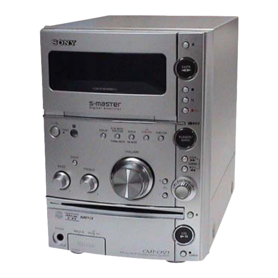
HCD-CPZ1 is the amplifier, CD player, tape
deck and tuner section in CMT-CPZ1.
US and foreign patents licensed from Dolby
Laboratories.
TE
L 13942296513
Amplifier section
European model:
DIN power output (rated): 60 + 60 watts (4 ohms at
Continuous RMS power output (reference):
Other models:
The following measured at AC 220 − 240 V, 50/60 Hz
DIN power output (rated) 60 + 60 watts
Continuous RMS power output (reference)
Inputs
ANALOG IN (stereo mini jack):
Outputs
CD DIGITAL OUT:
PHONES (stereo mini jack):
SPEAKER:
CD player section
www
System
.
Sony Corporation
9-879-454-02
Personal Audio Group
2005E05-1
Published by Sony Engineering Corporation
© 2005.05
http://www.xiaoyu163.com
Laser Diode Properties
1 kHz, DIN)
75 + 75 watts (4 ohms at
1 kHz, 10% THD)
(4 ohms at 1 kHz, DIN)
Frequency response
Wavelength
75 + 75 watts
(4 ohms at 1 kHz, 10%
Tape deck section
THD)
Recording system
Frequency response
Sensitivity 250 mV,
impedance 47 kilohms
Tuner section
Optical Wavelength:
FM stereo, FM/AM superheterodyne tuner
660 nm
FM tuner section
Tuning range
accepts headphones with
an impedance of 8 ohms or
Antenna
more
Antenna terminals
accepts impedance of
Intermediate frequency
4 ohms
AM tuner section
Tuning range
Compact disc and digital
audio system
x
ao
y
i
http://www.xiaoyu163.com
HCD-CPZ1
8
Model Name Using Similar Mechanism
CD
CD Mechanism Type
Section
Base Unit Name
Optical Pick-up Block Name
TAPE
Model Name Using Similar Mechanism
Q Q
Section
Tape Transport Mechanism Type
3
6 7
1 3
SPECIFICATIONS
Emission duration:
continuous
Laser Output: Less than
44.6 µW
(This output is the value
measurement at a distance
of 200 mm from the
objective lens surface on
the Optical Pick-up Block
with 7 mm aperture)
2 Hz − 20 kHz (±0.5 dB)
770 − 810nm
4-track 2-channel stereo
50 − 13,000 Hz (±3 dB),
using Sony TYPE I
cassettes
87.5 − 108.0 MHz
(50 kHz step)
FM lead antenna
75 ohms unbalanced
10.7 MHz
COMPACT DISC DECK RECEIVER
u163
.
2 9
9 4
2 8
AEP Model
Australian Model
NEW
CDM80BH-F1BD83
BU-F1BD83
KSM-215DCP
NEW
CMAL1Z-255A
1 5
0 5
8
2 9
9 4
European, model:
Other models:
Antenna
Antenna terminals
Intermediate frequency
General
Power requirements
European model:
Other models:
Power consumption
European model:
Other models:
Dimensions (w/h/d) (excl. speakers):
Mass (excl. speakers)
Amplifier/Tuner/Tape/CD section:
Design and specifications are subject to change
m
without notice.
co
9 9
UK Model
E Model
2 8
9 9
531 − 1,602 kHz
(with the tuning interval
set at 9 kHz)
531 − 1,602 kHz
(with the tuning interval
set at 9 kHz)
530 − 1,710 kHz
(with the tuning interval
set at 10 kHz)
AM loop antenna
External antenna terminal
450 kHz
230 V AC, 50/60 Hz
220 − 240 V AC, 50/60 Hz
60 watts
0.3 watts (in Power Saving
mode)
60 watts
Approx. 175 × 240 ×
295 mm
Approx. 3.8 kg
Advertisement
Table of Contents

Related Manuals for Sony HCD-CPZ1


Summary of Contents for Sony HCD-CPZ1
- Page 1 AEP Model UK Model Ver. 1.1 2005.05 E Model Australian Model HCD-CPZ1 is the amplifier, CD player, tape deck and tuner section in CMT-CPZ1. US and foreign patents licensed from Dolby Model Name Using Similar Mechanism Laboratories. CD Mechanism Type...
- Page 2 COMPONENTS IDENTIFIED BY MARK 0 OR DOTTED LINE WITH MARK 0 ON THE SCHEMATIC DIAGRAMS AND IN THE PARTS LIST ARE CRITICAL TO SAFE OPERATION. REPLACE THESE COMPONENTS WITH SONY PARTS WHOSE PART NUMBERS APPEAR AS SHOWN IN THIS MANUAL OR IN SUPPLEMENTS PUBLISHED BY SONY.
-
Page 3: Table Of Contents
HCD-CPZ1 3 7 63 1515 0 TABLE OF CONTENTS SERVICING NOTES EXPLODED VIEWS ..........4 8-1. Case Section ..............58 GENERAL 8-2. Mechanical Deck (Tape) Section ........59 ..............5 8-3. Front Panel Section ............60 8-4. Lid (TC) Section .............. 61 DISASSEMBLY 8-5. -
Page 4: Servicing Notes
HCD-CPZ1 Ver. 1.1 SECTION 1 SERVICING NOTES 3 7 63 1515 0 • MDDEL IDENTIFICATION NOTES ON HANDLING THE OPTICAL PICK-UP BLOCK OR BASE UNIT – Back Panel – The laser diode in the optical pick-up block may suffer electrostatic break-down because of the potential difference generated by the charged electrostatic load, etc. -
Page 5: General
HCD-CPZ1 SECTION 2 This section is extracted from instruction manual. GENERAL 3 7 63 1515 0 Main unit BUTTON DESCRIPTIONS ALPHABETICAL ORDER ?/1 (power) 1 ANALOG IN jack ws TAPE Z (eject) 4 BASS control wh TAPE nN (play) 5 CANCEL w;... -
Page 6: Disassembly
HCD-CPZ1 SECTION 3 DISASSEMBLY 3 7 63 1515 0 • This set can be disassembled in the order shown below. 3-1. DISASSEMBLY FLOW 3-2. CASE (Page 7) 3-3. FRONT PANEL SECTION (Page 7) 3-4. TC BOARD, 3-6. MAIN BOARD... -
Page 7: Case
HCD-CPZ1 3 7 63 1515 0 Note: Follow the disassembly procedure in the numerical order given. 3-2. CASE 4 case 2 three screws (B3) 1 two screws (case 3 TP2) 1 two screws (case 3 TP2) L 13942296513 3-3. FRONT PANEL SECTION... -
Page 8: Tc Board, Mechanical Deck (Cmal1Z-255A)
HCD-CPZ1 3 7 63 1515 0 3-4. TC BOARD, MECHANICAL DECK (CMAL1Z-255A) 6 terminal 5 four screws (B3) 1 wire (flat type) (8 core) 4 TC board 7 mechanical deck 3 connector (CMAL1Z-255A) 2 three screws (PTPWH 2) L 13942296513 3-5. -
Page 9: Main Board
HCD-CPZ1 Ver. 1.1 3 7 63 1515 0 3-6. MAIN BOARD 2 back panel 1 four screws (B3) 5 two connectors (CN201, CN202) 5 two connectors (CN300, CN306) 1 three screws (B3) 3 wire (flat type) (21 core) (CN302) -
Page 10: Chassis (Top)
HCD-CPZ1 3 7 63 1515 0 3-8. CHASSIS (TOP) 1 screw (BVTP 2.6 ) 3 three screws (BVTP 2.6) 2 lever (CL UP2) 4 two screws (P 2 × 10) 5 chassis (top) L 13942296513 u163 http://www.xiaoyu163.com... -
Page 11: Lever (Loading-L/R)
HCD-CPZ1 3 7 63 1515 0 3-9. LEVER (LOADING-L/R) spr-T (loading-R) spr-T (loading-L) L 13942296513 6 lever (loading-R) 3 two hooks 5 two hooks 4 lever (loading-L) PRECAUTION DURING LEVER (LOADING-R / L) INSTALLATION Align the horizontal position. lever (loading-L) -
Page 12: Lever (Disc Sensor), Lever (Disc Stop)
HCD-CPZ1 3 7 63 1515 0 3-10. LEVER (DISC SENSOR), LEVER (DISC STOP) 1 gear (cap) 2 gear (IDL-L) PRECAUTION DURING LEVER (DISC STOP) INSTALLATION chassis (top) hole 5 two hooks 3 two claws lever (disc stop) 6 lever (disc stop) -
Page 13: Bd Board
HCD-CPZ1 3 7 63 1515 0 3-12. BD BOARD Remove soldering 5 BD board from the four points. 3 sheet 4 wire (flat type) (23 core) (CN102) 2 wire (flat type) (16 core) (CN301) L 13942296513 3-13. BU SECTION... -
Page 14: Optical Pick-Up Block (Ksm-215Dcp)
HCD-CPZ1 3 7 63 1515 0 3-14. OPTICAL PICK-UP BLOCK (KSM-215DCP) 1 two screws (BTTP M2.6) 6 two insulators 7 optical pick-up block 2 two stoppers (BU) 4 two screws (KSM-215DCP) (PTPWH M2.6) 3 two coil springs (insulator) 5 two coil springs (insulator) -
Page 15: Close Lever
HCD-CPZ1 3 7 63 1515 0 3-16. CLOSE LEVER 1 washer (3-1-0.4) 5 close lever 3 claw 2 SPR-E lever close 4 shaft disc stop L 13942296513 3-17. LEVER (DIR), GEAR (IDL-B) 2 capstan retaining ring 3 pulley (gear) -
Page 16: Gear (Idl-C)
HCD-CPZ1 3 7 63 1515 0 3-18. GEAR (IDL-C) 3 gear (IDL-D) 2 two claws 4 three hooks 1 gear (IDL-F) 5 lever (gear loading) 7 gear (IDL-C) 6 claw L 13942296513 u163 http://www.xiaoyu163.com... -
Page 17: Test Mode
HCD-CPZ1 SECTION 4 TEST MODE 3 7 63 1515 0 [COMMON TEST MODE] [SHIP MODE (NO MEMORY CLEAR)] • This mode is used to check operations of Amplifier. • This mode moves the optical pick-up to the position durable Procedure: to vibration. - Page 18 HCD-CPZ1 Ver. 1.1 3 7 63 1515 0 [CD SERVO TEST MODE] • This mode used to ckeck operation of optical pick-up. Procedure: 1. Press the I/1 key to turn the power ON. 2. Press the [FUNCTION] key to select “CD”.
-
Page 19: Mechanical Adjustments
HCD-CPZ1 SECTION 5 SECTION 6 MECHANICAL ADJUSTMENTS 3 7 6 3 1 5 1 5 0 ELECTRICAL ADJUSTMENTS PRECAUTION 3. Mode: Playback DECK SECTION 0 dB=0.775 V CD SECTION 1. Clean the following parts with a denatured alcohol-moistened test tape... -
Page 20: Diagrams
HCD-CPZ1 Ver. 1.1 SECTION 7 3 7 6 3 1 5 1 5 0 DIAGRAMS 7-1. BLOCK DIAGRAM – CD SERVO/TAPE DECK/TUNER Section – OPTICAL PICK-UP BLOCK (KSM-215DCP) RFACO RFACI OPTICAL TRANSCEIVER DIGITAL DOUT IC981 CD-L AOUT1 112 (Page 21) -
Page 21: Block Diagram - Main Section
HCD-CPZ1 3 7 6 3 1 5 1 5 0 7-2. BLOCK DIAGRAM – MAIN Section – HEADPHONE J982 R-CH TAPE REC-L (Page 20) PHONES IC502 MUTING Q414 R-CH INPUT SELECT, ELECTRICAL VOLUME IC501 MUTING CD-L POWER DRIVER CONTROL... -
Page 22: Block Diagram - Panel/Key/Power Supply Section
HCD-CPZ1 3 7 6 3 1 5 1 5 0 7-3. BLOCK DIAGRAM – PANEL/KEY/POWER SUPPLY Section – LCD DRIVER IC951 D901 LED DRIVE LED STAND BY Q901 STANDBY DATA 59 LCD DATA LIQUID D902 60 LCD SCL CRYSTAL... - Page 23 HCD-CPZ1 Ver. 1.1 3 7 6 3 1 5 1 5 0 • Note for Printed Wiring Boards and Schematic Diagrams • Circuit Boards Location Note on Printed Wiring Board: Note on Schematic Diagram: • X : parts extracted from the component side.
-
Page 24: Printed Wiring Board - Bd Board
HCD-CPZ1 3 7 6 3 1 5 1 5 0 • See page 23 for Circuit Boards Location. 7-4. PRINTED WIRING BOARD – BD Board – :Uses unleaded solder. BD BOARD (COMPONENT SIDE) R279 M401 (SPINDLE) C401 S201 C405... -
Page 25: Schematic Diagram - Bd Board
HCD-CPZ1 Ver. 1.1 3 7 6 3 1 5 1 5 0 • See page 46 for Waveforms. • See page 46 for IC Block Diagrams. • See page 51 for IC Pin Function Description. 7-5. SCHEMATIC DIAGRAM – BD Board –... -
Page 26: Printed Wiring Board - Tc Board
HCD-CPZ1 3 7 6 3 1 5 1 5 0 • See page 23 for Circuit Boards Location. 7-6. PRINTED WIRING BOARD – TC Board – :Uses unleaded solder. • Semiconductor Location Ref. No. Location TC BOARD HRPE601 D681... -
Page 27: Schematic Diagram - Tc Board
HCD-CPZ1 3 7 6 3 1 5 1 5 0 • See page 46 for Waveforms. 7-7. SCHEMATIC DIAGRAM – TC Board – CN602 Q681 Q601,602,651,652 Q680,681,688 RT-1P141C-TP-1 PLAY SW REC/PB SWITCH REC/PB SWITCH R662 R REC Q692,694 Q691,693... -
Page 28: Printed Wiring Board - Driver Board
HCD-CPZ1 3 7 6 3 1 5 1 5 0 • See page 23 for Circuit Boards Location. • See page 46 for IC Block Diagrams. 7-8. PRINTED WIRING BOARD – DRIVER Board – 7-9. SCHEMATIC DIAGRAM – DRIVER Board –... -
Page 29: Printed Wiring Board - Main Board
HCD-CPZ1 • See page 23 for Circuit Boards Location. Ver. 1.1 7-10. PRINTED WIRING BOARD – MAIN Board – :Uses unleaded solder. 3 7 6 3 1 5 1 5 0 • Semiconductor Location SW POWER TC BOARD AMP BOARD... -
Page 30: Schematic Diagram - Main Board (1/2)
HCD-CPZ1 3 7 6 3 1 5 1 5 0 • See page 46 for IC Block Diagrams. 7-11. SCHEMATIC DIAGRAM – MAIN Board (1/2) – (1/2) CN302 A+5V AGND R IN AGND L IN P DOWN DGND R509 D+3.3V... -
Page 31: Schematic Diagram - Main Board (2/2)
HCD-CPZ1 Ver. 1.1 3 7 6 3 1 5 1 5 0 • See page 46 for Waveforms. • See page 46 for IC Block Diagrams. • See page 51 for IC Pin Function Description. 7-12. SCHEMATIC DIAGRAM – MAIN Board (2/2) –... -
Page 32: Schematic Diagram - Amp Board (1/2)
HCD-CPZ1 3 7 6 3 1 5 1 5 0 • See page 46 for Waveforms. • See page 46 for IC Block Diagrams. 7-13. SCHEMATIC DIAGRAM – AMP Board (1/2) – (1/2) R783 CN700 C731 OSC BUFFER L701... -
Page 33: Schematic Diagram - Amp Board (2/2)
HCD-CPZ1 3 7 6 3 1 5 1 5 0 • See page 46 for IC Block Diagrams. 7-14. SCHEMATIC DIAGRAM – AMP Board (2/2) – (2/2) EP702 POWER DRIVER (CHASSIS) EP701 IC707 CXD9774M C828 C839 C829 (CHASSIS) R704... -
Page 34: Printed Wiring Board - Amp Board
HCD-CPZ1 3 7 6 3 1 5 1 5 0 • See page 23 for Circuit Boards Location. 7-15. PRINTED WIRING BOARD – AMP Board – :Uses unleaded solder. • Semiconductor Location AMP BOARD AMP BOARD Ref. No. Location... -
Page 35: Printed Wiring Board - Sp Board
HCD-CPZ1 3 7 6 3 1 5 1 5 0 • See page 23 for Circuit Boards Location. 7-16. PRINTED WIRING BOARD – SP Board – 7-17. SCHEMATIC DIAGRAM – SP Board – :Uses unleaded solder. SP BOARD (COMPONENT SIDE) -
Page 36: Printed Wiring Board - Lcd Board
HCD-CPZ1 3 7 6 3 1 5 1 5 0 • See page 23 for Circuit Boards Location. 7-18. PRINTED WIRING BOARD – LCD Board – :Uses unleaded solder. LCD BOARD MAIN BOARD CN304 (Page 29) 1 3 9 4 2 2 9 6 5 1 3... -
Page 37: Schematic Diagram - Lcd Board
HCD-CPZ1 3 7 6 3 1 5 1 5 0 • See page 46 for Waveforms. 7-19. SCHEMATIC DIAGRAM – LCD Board – LCD951 LIQUID SRYSTAL DISPLAY JR955 1 3 9 4 2 2 9 6 5 1 3... -
Page 38: Printed Wiring Boards - Panel Section
HCD-CPZ1 • See page 23 for Circuit Boards Location. 7-20. PRINTED WIRING BOARDS – PANEL Section – :Uses unleaded solder. 3 7 6 3 1 5 1 5 0 • Semiconductor Location PANEL BOARD Ref. No. Location D901 G-12... -
Page 39: Schematic Diagram - Panel Section
HCD-CPZ1 3 7 6 3 1 5 1 5 0 7-21. SCHEMATIC DIAGRAM – PANEL Section – RV901 RV902 ROTARY ROTARY RV903 ENCODER ENCODER ROTARY ENCODER BASS TREBLE VOLUME RV904 PUSH ENTER (JOG) C911 FOLEDER B R932 R934 R936 R938 2.2k... -
Page 40: Printed Wiring Boards - Jack Section
HCD-CPZ1 3 7 6 3 1 5 1 5 0 • See page 23 for Circuit Boards Location. 7-22. PRINTED WIRING BOARDS – JACK Section – :Uses unleaded solder. MAIN BOARD CN303 (Page 29) HP/MD BOARD OPT BOARD (12) -
Page 41: Schematic Diagram - Jack Section
HCD-CPZ1 3 7 6 3 1 5 1 5 0 7-23. SCHEMATIC DIAGRAM – JACK Section – FB983 C992 C991 J982 0.022 0.022 PHONES FB982 C990 0.022 NO982 C986 HP R FB981 HP GND EP981 HP L HP DET... -
Page 42: Printed Wiring Board - Sw Power Board
HCD-CPZ1 3 7 6 3 1 5 1 5 0 • See page 23 for Circuit Boards Location. 7-24. PRINTED WIRING BOARD – SW POWER Board – :Uses unleaded solder. • Semiconductor Location Ref. No. Location AMP BOARD CN704... -
Page 43: Schematic Diagram - Sw Power Board
HCD-CPZ1 Ver. 1.1 3 7 6 3 1 5 1 5 0 • See page 51 for IC Pin Function Description. 7-25. SCHEMATIC DIAGRAM – SW POWER Board – SS11VL SS11VL -R11076 -R11076 D3SB60F3 470p 4700p T3.15AL LIVE 275V... -
Page 44: Printed Wiring Board - Sub Power Board
HCD-CPZ1 3 7 6 3 1 5 1 5 0 • See page 23 for Circuit Boards Location. 7-26. PRINTED WIRING BOARD – SUB POWER Board – :Uses unleaded solder. • Semiconductor Location Ref. No. Location SUB POWER BOARD... -
Page 45: Schematic Diagram - Sub Power Board
HCD-CPZ1 3 7 6 3 1 5 1 5 0 • See page 46 for IC Block Diagrams. 7-27. SCHEMATIC DIAGRAM – SUB POWER Board – LIVE NEUTRAL C992 RY991 NO991 0.01 250V (Page 43) D991 Q991 1SS355 2SC3052... -
Page 46: Http://Www.xiaoyu163.Com
HCD-CPZ1 3 7 6 3 1 5 1 5 0 • Waveforms • IC Block Diagrams – BD Board – – TC Board – – AMP Board – – BD Board – IC402 BA5947FM-E2 IC201 1 (LRCK) T601 4... - Page 47 HCD-CPZ1 3 7 63 1515 0 IC302 PST3629NR OUT 1 VDD 2 – VREF GND 3 IC501 BD3872FS LOUD LOUD SPEAKER SPEAKER EQUALIZER1 EQUALIZER2 LOGIC TREBLE1 BASS1 fo = 10 kHz fo = 80 Hz TREBLE2 BASS2 fo = 10 kHz...
- Page 48 HCD-CPZ1 3 7 63 1515 0 – AMP Board – IC701 PCM1802DBR SINGLE-END/ 5TH ORDER MODE1 VINL 1 DIFFERENTIAL DELTA-SIGMA MODE0 CONVERTER MODULATOR FMT1 VINR 2 FMT0 x16 1/64 (x1/128) SERIAL DECIMATION INTERFACE VREF1 3 SCKI FILTER & REFERENCE...
-
Page 49: Http://Www.xiaoyu163.Com
HCD-CPZ1 3 7 63 1515 0 IC705 CXD9788AR CLOCK CLOCK GENERATOR GENERATOR 36 XFSIIN (SECONDARY) (PRIMARY) XVSS 35 DVDD VSUBC 34 TEST 33 BFVSS VSSR OUTR2 32 BFVDD VDDR DATA FILTER & SAMPLING OUTR1 LINER GAIN ∆Σ LOW CUT... -
Page 50: Ao Y
HCD-CPZ1 3 7 63 1515 0 IC707, 708 CXD9774M GVDD B GVDD GVDD B BST B DVDD DREG DREG GND 1 PVDD B GATE PWM BP 2 PVDD B RECEIVER DRIVE OUT B TIMING GND 3 OUT B CONTROL DGND &... -
Page 51: Http://Www.xiaoyu163.Com
HCD-CPZ1 3 7 63 1515 0 • IC Pin Function Description BD BOARD IC201 CXD3014-201R (CD DSP) Pin No. Pin Name Description LRCK L/R sampling clock signal output terminal LRCKI L/R sampling clock signal input terminal PCMD Serial data output terminal... -
Page 52: Http://Www.xiaoyu163.Com
HCD-CPZ1 3 7 63 1515 0 Pin No. Pin Name Description FFDR Focus setvo drive signal (+) output to the coil/motor drive FRDR Focus servo drive signal (-) output to the coil/motor drive IOVDD1 Power supply terminal (+3.3V) AVDD0 Power supply terminal (+3.3V) -
Page 53: Http://Www.xiaoyu163.Com
HCD-CPZ1 3 7 63 1515 0 Pin No. Pin Name Description CLK2 MP3 serial data transfer clock signal input from the system controller SVSS Ground terminal SVDD Power supply terminal (+2.5V) JTAGTCK Not used JTAGTDI Not used JTAGTDO Not used... -
Page 54: Http://Www.xiaoyu163.Com
HCD-CPZ1 Ver. 1.1 3 7 63 1515 0 MAIN BOARD IC301 M30624MGP-A41FPU0 (SYSTEM CONTROLLER) Pin No. Pin Name Description AC DET Protect signal input terminal ST MUTE Tuner muting on/off control signal output terminal "H": muting on MP3 SSTB MP3 standby on/off control signal output terminal "L": standby... -
Page 55: Http://Www.xiaoyu163.Com
HCD-CPZ1 3 7 63 1515 0 Pin No. Pin Name Description S-MASTER DATA Serial data transfer output to the stream processor Shut down state input from the power driver "L": shut down S-MASTER SD S-MASTER RST Reset signal output to the stream processor... -
Page 56: Http://Www.xiaoyu163.Com
HCD-CPZ1 3 7 63 1515 0 Pin No. Pin Name Description MP3 IREQ MP3 data request signal output to the CD DSP MP3 XLAT MP3 serial data latch pulse output to the CD DSP MP3 REQ MP3 chip select signal output to the CD DSP... -
Page 57: Http://Www.xiaoyu163.Com
HCD-CPZ1 3 7 63 1515 0 SW POWER BOARD IC11 CXD9841P (POWER CONTROL) Pin No. Pin Name Description VSENSE AC line voltage detection terminal Feed back signal input terminal for frequency modulation of oscillator Connected to the external capacitor for oscillator duty/frequency setting... -
Page 58: Exploded Views
HCD-CPZ1 Ver. 1.1 SECTION 8 EXPLODED VIEWS 3 7 63 1515 0 NOTE: • -XX and -X mean standardized parts, so they • Items marked “*” are not stocked since they The components identified by mark 0 or dotted line with mark 0 are may have some difference from the original are seldom required for routine service. -
Page 59: Mechanical Deck (Tape) Section
HCD-CPZ1 3 7 63 1515 0 8-2. MECHANICAL DECK (TAPE) SECTION not supplied TC board lid (TC) section L 13942296513 flont panel section Ref. No. Part No. Description Remark Ref. No. Part No. Description Remark 2-588-354-01 LEVER (TC LOCK) -
Page 60: Front Panel Section
HCD-CPZ1 Ver. 1.1 3 7 63 1515 0 8-3. FRONT PANEL SECTION not supplied not supplied L 13942296513 Ref. No. Part No. Description Remark Ref. No. Part No. Description Remark 2-514-665-02 KNOB (UD) A-1087-733-A PANEL BOARD, COMPLETE 2-514-654-01 LID (MD LINK) -
Page 61: Lid (Tc) Section
HCD-CPZ1 3 7 63 1515 0 8-4. LID (TC) SECTION D951,D952 L 13942296513 LCD board not supplied LCD951 not supplied not supplied Ref. No. Part No. Description Remark Ref. No. Part No. Description Remark X-2048-618-1 LID (TC) ASSY 2-584-676-01 SPRING (TC), LEAF... -
Page 62: Chassis Section
HCD-CPZ1 Ver. 1.1 3 7 63 1515 0 8-5. CHASSIS SECTION AMP/POWER section not supplied not supplied not supplied CD (CDM80BH-F1BD83) L 13942296513 mechanism deck section-1 not supplied not supplied not supplied The components identified by mark 0 or dotted line with mark 0 are critical for safety. -
Page 63: Amp/Power Section
HCD-CPZ1 Ver. 1.1 3 7 63 1515 0 8-6. AMP/POWER SECTION SW POWER board not supplied not supplied L 13942296513 not supplied not supplied The components identified by mark 0 or dotted line with mark 0 are critical for safety. -
Page 64: Cd Mechanism Deck Section-1 (Cdm80Bh-F1Bd83)
HCD-CPZ1 3 7 63 1515 0 8-7. CD MECHANISM DECK SECTION-1 (CDM80BH-F1BD83) CD mechanism deck section-2 M701 (CDM80BH-F1BD83) L 13942296513 CD mechanism deck section-3 (CDM80BH-F1BD83) base unit section (BU-F1BD83) Ref. No. Part No. Description Remark Ref. No. Part No. -
Page 65: Cd Mechanism Deck Section-2 (Cdm80Bh-F1Bd83)
HCD-CPZ1 3 7 63 1515 0 8-8. CD MECHANISM DECK SECTION-2 (CDM80BH-F1BD83) L 13942296513 Ref. No. Part No. Description Remark Ref. No. Part No. Description Remark 4-245-627-01 WASHER (6-2.7-0.4) 4-245-640-01 GEAR (CAP) 4-245-637-11 ROLLER, RUBBER 1-452-925-21 MAGNET ASSY 4-245-649-01 GEAR (IDL-I) -
Page 66: Cd Mechanism Deck Section-3 (Cdm80Bh-F1Bd83)
HCD-CPZ1 3 7 63 1515 0 8-9. CD MECHANISM DECK SECTION-3 (CDM80BH-F1BD83) not supplied L 13942296513 not supplied Ref. No. Part No. Description Remark Ref. No. Part No. Description Remark 4-245-643-01 GEAR (IDL-C) 4-245-640-01 GEAR (CAP) X-4956-147-1 CHASSIS (BOTTOM) ASSY... -
Page 67: Base Unit Section (Bu-F1Bd83)
HCD-CPZ1 3 7 63 1515 0 8-10. BASE UNIT SECTION (BU-F1BD83) (including spindle motor (M401), sled motor (M402)) not supplied not supplied L 13942296513 (sled motor (M402)) (spindle motor (M401)) S201 The components identified by mark 0 or dotted line with mark 0 are critical for safety. -
Page 68: Electrical Parts List
HCD-CPZ1 Ver. 1.1 SECTION 9 3 7 63 1515 0 ELECTRICAL PARTS LIST NOTE: • Due to standardization, replacements in the • Items marked “*” are not stocked since they The components identified by mark 0 or dotted line with mark 0 are parts list may be different from the parts are seldom required for routine service. - Page 69 HCD-CPZ1 Ver. 1.1 3 7 63 1515 0 Ref. No. Part No. Description Remark Ref. No. Part No. Description Remark C799 1-107-826-11 CERAMIC CHIP 0.1uF L759 1-456-813-11 COIL, AIR-CORE C806 1-107-826-11 CERAMIC CHIP 0.1uF L760 1-456-680-11 INDUCTOR 10uH L761...
- Page 70 HCD-CPZ1 Ver. 1.1 3 7 63 1515 0 Ref. No. Part No. Description Remark Ref. No. Part No. Description Remark R757 1-216-864-11 SHORT CHIP C201 1-128-995-21 ELECT CHIP 100uF R758 1-216-864-11 SHORT CHIP C202 1-164-360-11 CERAMIC CHIP 0.1uF R759...
- Page 71 HCD-CPZ1 Ver. 1.1 DRIVER HP/MD 3 7 63 1515 0 Ref. No. Part No. Description Remark Ref. No. Part No. Description Remark C451 1-162-968-11 CERAMIC CHIP 0.0047uF 10% R291 1-216-809-11 METAL CHIP 1/10W C452 1-162-966-11 CERAMIC CHIP 0.0022uF 10%...
- Page 72 HCD-CPZ1 Ver. 1.1 HP/MD MAIN 3 7 63 1515 0 Ref. No. Part No. Description Remark Ref. No. Part No. Description Remark R953 1-216-833-11 METAL CHIP 1/10W < SHORT > R954 1-216-809-11 METAL CHIP 1/10W R955 1-216-809-11 METAL CHIP...
- Page 73 HCD-CPZ1 Ver. 1.1 MAIN 3 7 63 1515 0 Ref. No. Part No. Description Remark Ref. No. Part No. Description Remark C510 1-126-960-11 ELECT CN305 1-784-780-11 CONNECTOR, FFC 19P C511 1-126-964-11 ELECT 10uF * CN306 1-815-448-11 PIN, CONNECTOR (PWB) 7P...
- Page 74 HCD-CPZ1 Ver. 1.1 MAIN 3 7 63 1515 0 Ref. No. Part No. Description Remark Ref. No. Part No. Description Remark R370 1-216-809-11 METAL CHIP 1/10W < RESISTOR > R371 1-216-809-11 METAL CHIP 1/10W R301 1-216-833-11 METAL CHIP 1/10W...
- Page 75 HCD-CPZ1 MAIN PANEL 3 7 63 1515 0 Ref. No. Part No. Description Remark Ref. No. Part No. Description Remark R477 1-216-833-11 METAL CHIP 1/10W A-1087-733-A PANEL BOARD, COMPLETE R478 1-216-833-11 METAL CHIP 1/10W ********************** R490 1-216-821-11 METAL CHIP...
- Page 76 HCD-CPZ1 Ver. 1.1 PANEL SUB PANEL SUB POWER SW POWER 3 7 63 1515 0 Ref. No. Part No. Description Remark Ref. No. Part No. Description Remark R932 1-216-825-11 METAL CHIP 2.2K 1/10W < RESISTOR > R933 1-216-829-11 METAL CHIP 4.7K...
- Page 77 HCD-CPZ1 Ver. 1.1 SW POWER 3 7 63 1515 0 Ref. No. Part No. Description Remark Ref. No. Part No. Description Remark 0 C3 0 Q12 1-165-528-11 MYLAR 0.1uF 275V 6-551-319-01 FET 2SK3563 (LB2SONY) 0 C4 1-119-886-51 CERAMIC 470PF...
- Page 78 HCD-CPZ1 3 7 63 1515 0 Ref. No. Part No. Description Remark Ref. No. Part No. Description Remark C635 1-126-960-11 ELECT R603 1-216-821-11 METAL CHIP 1/10W C640 1-126-947-11 ELECT 47uF R604 1-216-833-11 METAL CHIP 1/10W C641 1-126-961-11 ELECT 2.2uF...
- Page 79 HCD-CPZ1 Ver. 1.1 3 7 63 1515 0 Ref. No. Part No. Description Remark Ref. No. Part No. Description Remark MISCELLANEOUS ************** 1-796-456-41 DECK, MECHANICAL (CMAL1Z-255A) 1-773-106-11 WIRE (FLAT TYPE) (19 CORE) 1-773-120-11 WIRE (FLAT TYPE) (19 CORE) 1-769-912-11 WIRE (FLAT TYPE) (9 CORE)
- Page 80 HCD-CPZ1 3 7 63 1515 0 REVISION HISTORY Clicking the version allows you to jump to the revised page. Also, clicking the version at the upper right on the revised page allows you to jump to the next revised page.
Need help?
Do you have a question about the HCD-CPZ1 and is the answer not in the manual?
Questions and answers