
Subscribe to Our Youtube Channel
Related Manuals for NXP Semiconductors QorIQ LS1046ARDB


Summary of Contents for NXP Semiconductors QorIQ LS1046ARDB
- Page 1 NXP Semiconductors Document Number: LS1046ARDBRM Reference Manual Rev. 2, 30 May 2019 QorIQ LS1046A Reference Design Board Reference Manual Supports LS1046ARDB Revision B...
-
Page 2: Table Of Contents
3.11 SerDes1 Reference Clock2 Setting Register (REG_SD1REFCLK_SEL)......52 3.12 Ethernet Controller 2 Connection Control Register (REG_RGMII_1588_SEL)..... 53 3.13 1588 Clock Source Control Register (REG_1588_CLK_SEL)..........54 3.14 STATUS LED Control Register (REG_STATUS_LED)............55 QorIQ LS1046A Reference Design Board Reference Manual, Rev. 2, 30 May 2019 NXP Semiconductors... - Page 3 3.17 VDD Voltage Control Register Take Effect Enable Register (REG_VDD_EN)....... 58 3.18 VDD Voltage Control Register (REG_VDD_SEL)..............59 3.19 SFP+ Module Tx Enable Register (REG_SFP_TXEN)............60 3.20 SFP+ Module Status Register (REG_SFP_STATUS)............61 Appendix A Revision History................63 QorIQ LS1046A Reference Design Board Reference Manual, Rev. 2, 30 May 2019 NXP Semiconductors...
- Page 4 Figure 14. SDHC connections..............................32 Figure 15. UART interface................................33 Figure 16. I2C scheme.................................34 Figure 17. JTAG architecture.................................35 Figure 18. CMSIS-DAP................................36 Figure 19. Thermal management system.............................37 QorIQ LS1046A Reference Design Board Reference Manual, Rev. 2, 30 May 2019 NXP Semiconductors...
- Page 5 Table 16. Temperature sensor..............................37 Table 17. DIP switch settings................................ 38 Table 18. LS1046ARDB LEDs..............................39 Table 19. LS1046A processor configuration pins......................... 41 Table 20. Revision history................................63 QorIQ LS1046A Reference Design Board Reference Manual, Rev. 2, 30 May 2019 NXP Semiconductors...
-
Page 6: Chapter 1 Ls1046Ardb Overview
Integrated flash controller JTAG Joint Test Action Group Low-dropout Light-emitting diode Media access control Multimedia card Media-independent interface Mass storage device Table continues on the next page... QorIQ LS1046A Reference Design Board Reference Manual, Rev. 2, 30 May 2019 NXP Semiconductors... -
Page 7: Related Documentation
LS1046ARDB. Some of the documents listed below may be available only under a non-disclosure agreement (NDA). To request access to these documents, contact your local field applications engineer (FAE) or sales representative. QorIQ LS1046A Reference Design Board Reference Manual, Rev. 2, 30 May 2019 NXP Semiconductors... -
Page 8: Block Diagram
(usually JTAG) while connected to a developer workstation through Ethernet or 1.3 Block diagram The figure below shows the LS1046ARDB block diagram. QorIQ LS1046A Reference Design Board Reference Manual, Rev. 2, 30 May 2019 NXP Semiconductors... -
Page 9: Board Features
Processor feature used Description Processor QorIQ LS1046A processor NOTE For details on the LS1046A processor, see QorIQ LS1046A Reference Manual. Table continues on the next page... QorIQ LS1046A Reference Design Board Reference Manual, Rev. 2, 30 May 2019 NXP Semiconductors... - Page 10 • USB2: Supports a USB 3.0 micro-AB connector configured in the On-The-Go (OTG) mode, by default • USB3: Connects to the mini-PCIe slot Table continues on the next page... QorIQ LS1046A Reference Design Board Reference Manual, Rev. 2, 30 May 2019 NXP Semiconductors...
- Page 11 PMIC, clock generator, current monitor, thermal monitor, EEPROM, mini-PCIe slot, and one PCIe slot • I2C4: Controls the other PCIe slot and RTC Table continues on the next page... QorIQ LS1046A Reference Design Board Reference Manual, Rev. 2, 30 May 2019 NXP Semiconductors...
- Page 12 • 3.3 V for RGMII and SGMII PHYs, SDHC connector, and PCIe slots • 3.3/1.5 V for mini-PCIe slot • 5 V for USB port • 3.3/1.8 V for CPLD Table continues on the next page... QorIQ LS1046A Reference Design Board Reference Manual, Rev. 2, 30 May 2019 NXP Semiconductors...
- Page 13 • Three DIP switches for quick board configuration NOTE See QorIQ LS1046A Reference Design Board Getting Started Guide for more details on LS1046ARDB DIP switches. Table continues on the next page... QorIQ LS1046A Reference Design Board Reference Manual, Rev. 2, 30 May 2019 NXP Semiconductors...
-
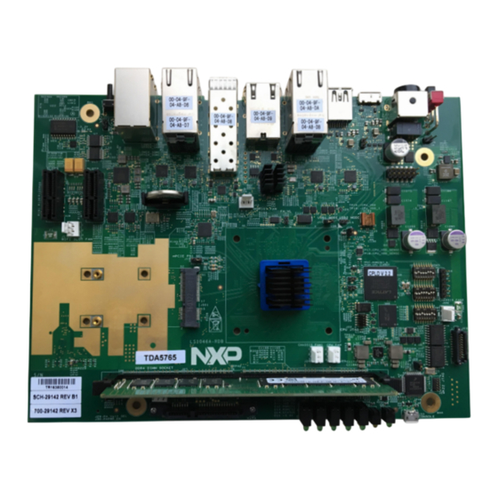
Page 14: Board Top/Bottom Views
1.5 Board top/bottom views The figure below shows the LS1046ARDB top view. Figure 2. LS1046ARDB top view The figure below shows the LS1046ARDB bottom view. QorIQ LS1046A Reference Design Board Reference Manual, Rev. 2, 30 May 2019 NXP Semiconductors... -
Page 15: Figure 3. Ls1046Ardb Bottom View
Board top/bottom views Figure 3. LS1046ARDB bottom view QorIQ LS1046A Reference Design Board Reference Manual, Rev. 2, 30 May 2019 NXP Semiconductors... -
Page 16: Chapter 2 Ls1046Ardb Functional Description
12 V power for correct operation of the LS1046A processor, DDR4 UDIMM, PHYs, and numerous other peripherals. The figure below shows the LS1046ARDB power supply block diagram. QorIQ LS1046A Reference Design Board Reference Manual, Rev. 2, 30 May 2019 NXP Semiconductors... -
Page 17: Primary Power Supply
Figure 5. Pinout details toward LS1046ARDB 2.1.2 Secondary power supplies The table below describes the LS1046ARDB power supply devices that generate secondary power supplies on the board. QorIQ LS1046A Reference Design Board Reference Manual, Rev. 2, 30 May 2019 NXP Semiconductors... -
Page 18: Table 4. Ls1046Ardb Power Supply Devices
• Supply for LT3065 (U12) power supply device SW4LX: +SVDD Filtered supply for processor SVDD (1/0.9 V at 1 A) Table continues on the next page... QorIQ LS1046A Reference Design Board Reference Manual, Rev. 2, 30 May 2019 NXP Semiconductors... -
Page 19: Power Supply Sequence
Shunt resistor value 0.001 Ω INA220 All other power supplies of the board are considered as low-current/incidental supplies and therefore, they are not instrumented for power measurement. QorIQ LS1046A Reference Design Board Reference Manual, Rev. 2, 30 May 2019 NXP Semiconductors... -
Page 20: Clocks
• Operating voltage: 3.3 V SYSCLK_18 LS1046A processor (secondary • Frequency: 100 MHz system clock) • Output type: LVCMOS • Operating voltage: 1.8 V Table continues on the next page... QorIQ LS1046A Reference Design Board Reference Manual, Rev. 2, 30 May 2019 NXP Semiconductors... - Page 21 • Operating voltage: 3.3 V 25MHZ_CPLD CPLD (reference clock) • Frequency: 25 MHz • Output type: LVCMOS • Operating voltage: 3.3 V Table continues on the next page... QorIQ LS1046A Reference Design Board Reference Manual, Rev. 2, 30 May 2019 NXP Semiconductors...
- Page 22 • Output type: LVCMOS • Operating voltage: 3.3 V U36: CPLD RTCCLK_18 LS1046A processor (RTC) • Frequency: 32.768 kHz • Output type: LVCMOS • Operating voltage: 1.8 V QorIQ LS1046A Reference Design Board Reference Manual, Rev. 2, 30 May 2019 NXP Semiconductors...
-
Page 23: Ddr Interface
The LS1046ARDB DDR interface can work with any JEDEC-compliant, 288-pin, DDR4 UDIMM or RDIMM module. The DIMM used in the board is only a representative DIMM (MTA18ASF1G72AZ-2G3B1). QorIQ LS1046A Reference Design Board Reference Manual, Rev. 2, 30 May 2019 NXP Semiconductors... -
Page 24: Serdes Interface
— SLOT 3: Standard PCIe x1 • One SATA 3.0 connector • One SFP + module with XFI retimer The following figure shows the SerDes architecture with PCI Express support. QorIQ LS1046A Reference Design Board Reference Manual, Rev. 2, 30 May 2019 NXP Semiconductors... -
Page 25: Figure 8. Serdes Architecture
PCIe slots 1 and 2 PRECISION 2UWC Molex 679100002 Mini-PCIe slot Realtek RTL8211FS SGMII PHY 1 Realtek RTL8211FS SGMII PHY 2 Table continues on the next page... QorIQ LS1046A Reference Design Board Reference Manual, Rev. 2, 30 May 2019 NXP Semiconductors... -
Page 26: Pci Express Support
The mini-PCIe card slot supports: • USB 2.0 • PCIe • I2C Configure the Wi-Fi module on the mini-PCIe slot as per the configuration given in the table below. QorIQ LS1046A Reference Design Board Reference Manual, Rev. 2, 30 May 2019 NXP Semiconductors... -
Page 27: Sgmii Support
L: Transmit or receive activity R: Link (any speed) LVDD (1.8 V) MAC4 P2 top L: Transmit or receive activity R: Link (any speed) Table continues on the next page... QorIQ LS1046A Reference Design Board Reference Manual, Rev. 2, 30 May 2019 NXP Semiconductors... -
Page 28: Ieee-1588 Support
(2.5 V) domain respectively and are used to control separate PHY transceiver devices. The EMI1 bus is connected to the four Realtek (RTL8211FS) PHYs. The EMI2 bus is connected to the Aquantia (AQR107) PHY. The EMI routing architecture is shown in the figure below. QorIQ LS1046A Reference Design Board Reference Manual, Rev. 2, 30 May 2019 NXP Semiconductors... -
Page 29: Usb Interface
5 V power at up to 1.2 A. The power enable and power-fault-detect pins are connected to the LS1046A processor via CPLD for individual port management. The figure below shows the LS1046ARDB USB architecture. QorIQ LS1046A Reference Design Board Reference Manual, Rev. 2, 30 May 2019 NXP Semiconductors... -
Page 30: Ifc Interface
• Supports 28-bit addressing and 16-bit data bus • Supports 512 MB SLC NAND flash memory (async/sync - ONFI 1.0 compatible) The figure below shows the IFC block diagram. QorIQ LS1046A Reference Design Board Reference Manual, Rev. 2, 30 May 2019 NXP Semiconductors... -
Page 31: Qspi Interface
NX3DV42GU (U514, U512, and U513) drive the SDHC signals to eMMC or SD card. The figure below shows the SDHC signal connections supported on the LS1046ARDB. QorIQ LS1046A Reference Design Board Reference Manual, Rev. 2, 30 May 2019 NXP Semiconductors... -
Page 32: Uart Interface
Pin 8 DAT0 Data signal 0 Pin 9 DAT1 Data signal 1 2.11 UART interface The figure below shows the LS1046ARDB universal asynchronous receiver/transmitter (UART) connections. QorIQ LS1046A Reference Design Board Reference Manual, Rev. 2, 30 May 2019 NXP Semiconductors... -
Page 33: I2C Interface
• The level shifter device (PCA9306DCUR) is used on the LS1046ARDB I2C1 bus, to convert the LS1046A 3.3 V to 2.5 V signals for the SPD The figure below shows the overall I2C scheme connections. QorIQ LS1046A Reference Design Board Reference Manual, Rev. 2, 30 May 2019 NXP Semiconductors... -
Page 34: Figure 16. I2C Scheme
0x4C ON Semiconductor ADT7461 Thermal monitor 0x51 Micron DDR module SPD 0x69 Clock generator 6V49205BNLGI 0x08 VR500V8 NXP Semiconductors 0x40 Texas Instruments Current/power monitor INA220AIDGST 0x18 DS110DF111 Texas Instruments XFI1 retimer I2C address is Mini-PCIe x1 slot defined by the... -
Page 35: Jtag Interface
Real-time clock (RTC) PCF2129AT Semiconductor 2.13 JTAG interface The ARM/JTAG architecture is shown in the figure below. LS1046A Buffer& Level K22 MCU shifter Figure 17. JTAG architecture QorIQ LS1046A Reference Design Board Reference Manual, Rev. 2, 30 May 2019 NXP Semiconductors... -
Page 36: Cmsis-Dap Interface
(through THERM_WARN_B and THERM_FAULT_B interrupt signals) to the processor. These interrupts can be used to power down the system to protect the processor from over-temperature damage. The figure below shows thermal management system in the LS1046ARDB. QorIQ LS1046A Reference Design Board Reference Manual, Rev. 2, 30 May 2019 NXP Semiconductors... -
Page 37: Dip Switches
For LS1046ARDB DIP switches: • "ON" setting corresponds to 1 • "OFF" setting corresponds to 0 The table below describes the DIP switch settings. QorIQ LS1046A Reference Design Board Reference Manual, Rev. 2, 30 May 2019 NXP Semiconductors... -
Page 38: Table 17. Dip Switch Settings
• 1: SerDes1 clock 2 is sourced from a 156.25 MHz clock source (default setting) SW4[6] Unused Reserved with 0 as the default setting SW_EVDD_SEL Table continues on the next page... QorIQ LS1046A Reference Design Board Reference Manual, Rev. 2, 30 May 2019 NXP Semiconductors... -
Page 39: Leds
Description Green +3.3V • OFF: 3.3 V power is OFF Green Chassis POWER • ON: 3.3 V power is supplied Table continues on the next page... QorIQ LS1046A Reference Design Board Reference Manual, Rev. 2, 30 May 2019 NXP Semiconductors... - Page 40 Indicates the status of the Wi-Fi card used on the mini-PCIe slot. Depends on the Wi-Fi card used. Yellow Chassis STATUS Controlled through CPLD register, REG_STAT US_LED. See "Programming Model" chapter for more details. QorIQ LS1046A Reference Design Board Reference Manual, Rev. 2, 30 May 2019 NXP Semiconductors...
-
Page 41: Processor Configuration
Sets to 1 on POR by CPLD or IFC_OE_B, IFC_WP0_B resistors NOTE This section does not cover non-processor configuration signals, which are handled using statically-driven signals through registers. QorIQ LS1046A Reference Design Board Reference Manual, Rev. 2, 30 May 2019 NXP Semiconductors... -
Page 42: Chapter 3 Programming Model
VDD Voltage Control Register Take Effect Enable Register (REG_ VDD_EN) VDD Voltage Control Register (REG_VDD_SEL) SFP+ Module Tx Enable Register (REG_SFP_TXEN) SFP+ Module Status Register (REG_SFP_STATUS) QorIQ LS1046A Reference Design Board Reference Manual, Rev. 2, 30 May 2019 NXP Semiconductors... -
Page 43: Cpld Major Revision Register (Cpld_Ver)
CPLD_VER CPLD major revision number CPLD_VER Reserved 3.2 CPLD Minor Revision Register (CPLD_VER_SUB) Offset Register Offset CPLD_VER_SUB Function Read this register to get CPLD minor revision. QorIQ LS1046A Reference Design Board Reference Manual, Rev. 2, 30 May 2019 NXP Semiconductors... -
Page 44: Pcba Revision Register (Pcba_Ver)
Read this register to get PCBA revision. Diagram Bits PCBA_VER Reserved Reset 1000 0000 Fields Field Function PCBA_VER PCBA revision number PCBA_VER Table continues on the next page... QorIQ LS1046A Reference Design Board Reference Manual, Rev. 2, 30 May 2019 NXP Semiconductors... -
Page 45: System Hardware Reset Register (Reg_System_Rst)
Reserved Reset 0000000 Fields Field Function SYSTEM_RST SYSTEM_RST System hardware reset (not reset value of CPLD registers) 0b: Reset deassserted (default value) 1b: Reset asserted Reserved QorIQ LS1046A Reference Design Board Reference Manual, Rev. 2, 30 May 2019 NXP Semiconductors... -
Page 46: Cpld Registers Take Effect Enable Register (Reg_Soft_Mux_On)
UART1_SEL_EN UART1_SEL_E UART1 connection control register enable 0b: REG_UART1_SEL Register no effect (default value) 1b: REG_ UART1_SEL Register take effect Table continues on the next page... QorIQ LS1046A Reference Design Board Reference Manual, Rev. 2, 30 May 2019 NXP Semiconductors... -
Page 47: Rcw Source Location Por Register 1 (Reg_Cfg_Rcw_Src1)
1b: REG_SD_EMMC Register take effect 3.6 RCW Source Location POR Register 1 (REG_CFG_RCW_ SRC1) Offset Register Offset REG_CFG_RCW_SRC1 5h Function Use this register to configure RCW source POR bits 0-7. QorIQ LS1046A Reference Design Board Reference Manual, Rev. 2, 30 May 2019 NXP Semiconductors... -
Page 48: Rcw Source Location Por Register 2 (Reg_Cfg_Rcw_Src2)
Others: Reserved 3.7 RCW Source Location POR Register 2 (REG_CFG_RCW_ SRC2) Offset Register Offset REG_CFG_RCW_SRC2 6h Function Use this register to configure RCW source POR bits 8. QorIQ LS1046A Reference Design Board Reference Manual, Rev. 2, 30 May 2019 NXP Semiconductors... -
Page 49: Qspi Flash Bank Setting Register (Reg_Qspi_Bank)
0100_1XXX_X: Hard-coded RCW Others: Reserved Reserved 3.8 QSPI Flash Bank Setting Register (REG_QSPI_BANK) Offset Register Offset REG_QSPI_BANK Function Use this register to configure QSPI Flash bank. QorIQ LS1046A Reference Design Board Reference Manual, Rev. 2, 30 May 2019 NXP Semiconductors... -
Page 50: System Clock Por Register (Reg_Sysclk_Sel)
DEV#0 DEV#0 DEV#1 DEV#0 Others Reserved Reserved 3.9 System clock POR Register (REG_SYSCLK_SEL) Offset Register Offset REG_SYSCLK_SEL Function Use this register to configure system clock POR. QorIQ LS1046A Reference Design Board Reference Manual, Rev. 2, 30 May 2019 NXP Semiconductors... -
Page 51: Uart1 Connection Control Register (Reg_Uart1_Sel)
0: Differential clock (default value) 1: Single-ended Clock Reserved 3.10 UART1 Connection Control Register (REG_UART1_SEL) Offset Register Offset REG_UART1_SEL Function Use this register to configure UART1 connection. QorIQ LS1046A Reference Design Board Reference Manual, Rev. 2, 30 May 2019 NXP Semiconductors... -
Page 52: Serdes1 Reference Clock2 Setting Register (Reg_Sd1Refclk_Sel)
1: UART1 to CMSIS-DAP (default value) Reserved 3.11 SerDes1 Reference Clock2 Setting Register (REG_SD1R EFCLK_SEL) Offset Register Offset REG_SD1REFCLK_SEL Ah Function Use this register to configure SerDes1 reference clock 2 frequency. QorIQ LS1046A Reference Design Board Reference Manual, Rev. 2, 30 May 2019 NXP Semiconductors... -
Page 53: Ethernet Controller 2 Connection Control Register (Reg_Rgmii_1588_Sel)
1: 156.25 MHz (default value) Reserved 3.12 Ethernet Controller 2 Connection Control Register (REG_ RGMII_1588_SEL) Offset Register Offset REG_RGMII_1588_SEL Function Use this register to configure ethernet controller 2 connection. QorIQ LS1046A Reference Design Board Reference Manual, Rev. 2, 30 May 2019 NXP Semiconductors... -
Page 54: 1588 Clock Source Control Register (Reg_1588_Clk_Sel)
1: RGMII PHY (default value) Reserved 3.13 1588 Clock Source Control Register (REG_1588_CLK_ SEL) Offset Register Offset REG_1588_CLK_SEL Function Use this register to configure 1588 clock source. QorIQ LS1046A Reference Design Board Reference Manual, Rev. 2, 30 May 2019 NXP Semiconductors... -
Page 55: Status Led Control Register (Reg_Status_Led)
0: From on-board clock generator (default value) 1: From 1588 Interface connector Reserved 3.14 STATUS LED Control Register (REG_STATUS_LED) Offset Register Offset REG_STATUS_LED Function Use this register to control STATUS LED. QorIQ LS1046A Reference Design Board Reference Manual, Rev. 2, 30 May 2019 NXP Semiconductors... -
Page 56: System Hardware Reset Register (Reg_Global_Rst)
3.15 System Hardware Reset Register (REG_GLOBAL_RST) Offset Register Offset REG_GLOBAL_RST Function Use this register to implement system hardware reset and initialize the value of CPLD registers. QorIQ LS1046A Reference Design Board Reference Manual, Rev. 2, 30 May 2019 NXP Semiconductors... -
Page 57: Sd Or Emmc Interface Control Register (Reg_Sd_Emm)
1: Reset asserted Reserved 3.16 SD or EMMC Interface Control Register (REG_SD_EMM) Offset Register Offset REG_SD_EMM Function Use this register to select SD or eMMC interface. QorIQ LS1046A Reference Design Board Reference Manual, Rev. 2, 30 May 2019 NXP Semiconductors... -
Page 58: Vdd Voltage Control Register Take Effect Enable Register (Reg_Vdd_En)
3.17 VDD Voltage Control Register Take Effect Enable Register (REG_VDD_EN) Offset Register Offset REG_VDD_EN Function Use this register to enable REG_VDD_SEL register value to take effect. QorIQ LS1046A Reference Design Board Reference Manual, Rev. 2, 30 May 2019 NXP Semiconductors... -
Page 59: Vdd Voltage Control Register (Reg_Vdd_Sel)
0: REG_VDD_SEL register no effect (default value) 1: REG_VDD_SEL register take effect Reserved 3.18 VDD Voltage Control Register (REG_VDD_SEL) Offset Register Offset REG_VDD_SEL Function Use this register to control VDD voltage. QorIQ LS1046A Reference Design Board Reference Manual, Rev. 2, 30 May 2019 NXP Semiconductors... -
Page 60: Sfp+ Module Tx Enable Register (Reg_Sfp_Txen)
1b: VDD 0.9 V Reserved 3.19 SFP+ Module Tx Enable Register (REG_SFP_TXEN) Offset Register Offset REG_SFP_TXEN Function Use this register to control SFP+ module Tx enable. QorIQ LS1046A Reference Design Board Reference Manual, Rev. 2, 30 May 2019 NXP Semiconductors... -
Page 61: Sfp+ Module Status Register (Reg_Sfp_Status)
1b: Tx disable Reserved 3.20 SFP+ Module Status Register (REG_SFP_STATUS) Offset Register Offset REG_SFP_STATUS Function Use this register to read the status of the SFP+ module. QorIQ LS1046A Reference Design Board Reference Manual, Rev. 2, 30 May 2019 NXP Semiconductors... - Page 62 0b: Normal operation (default value) 1b: Transmitter fault XFI1_RETIMER_LOS XFI1_RETIMER XFI1 retimer signal loss _LOS 0b: A valid signal is present (default value) 1b: The signal is lost Reserved QorIQ LS1046A Reference Design Board Reference Manual, Rev. 2, 30 May 2019 NXP Semiconductors...
-
Page 63: Appendix A Revision History
03/2017 Board features on page 9 Updated core frequency to 1.8 GHz in Table 3. LS1046ARDB features on page 9 Rev. 0 09/2016 Initial public release QorIQ LS1046A Reference Design Board Reference Manual, Rev. 2, 30 May 2019 NXP Semiconductors... - Page 64 How To Reach Us Information in this document is provided solely to enable system and software implementers to use NXP products. There are no express or implied copyright licenses granted hereunder to Home Page: design or fabricate any integrated circuits based on the information in this document. NXP nxp.com reserves the right to make changes without further notice to any products herein.
Need help?
Do you have a question about the QorIQ LS1046ARDB and is the answer not in the manual?
Questions and answers