Panasonic CF-T5 Service Manual
Hide thumbs
Also See for CF-T5:
- Operating instructions manual (40 pages) ,
- Supplementary instructions manual (12 pages) ,
- Reference manual (103 pages)
Table of Contents
Advertisement
Quick Links
Model No. CF-T5LWETZ
1: Operation System
B: Microsoft
2: Area
M: Refer to above area table
1 2
®
®
Windows
XP Professional
Personal Computer
This is the Service Manual for
the following areas.
M ...for U.S.A. and Canada
© 2006 Matsushita Electric Industrial Co., Ltd. All rights reserved.
Unauthorized copying and distribution is a violation of law.
ORDER NO. CPD0610202C1
CF-T5
Advertisement
Table of Contents

Subscribe to Our Youtube Channel
Related Manuals for Panasonic CF-T5


Summary of Contents for Panasonic CF-T5
- Page 1 ORDER NO. CPD0610202C1 Personal Computer CF-T5 This is the Service Manual for the following areas. M …for U.S.A. and Canada Model No. CF-T5LWETZ 1: Operation System ® ® B: Microsoft Windows XP Professional 2: Area M: Refer to above area table ©...
-
Page 5: Table Of Contents
CONTENTS 1. Specifications 2. Names and Functions of Parts 3. Block Diagram 4. Diagnosis Procedure 5. Power-On Self Test (Boot Check) 6. List of Error Codes <Only when the port replicator is connected> 7. Self Diagnosis Test 8. Wiring Connection Diagram 9. -
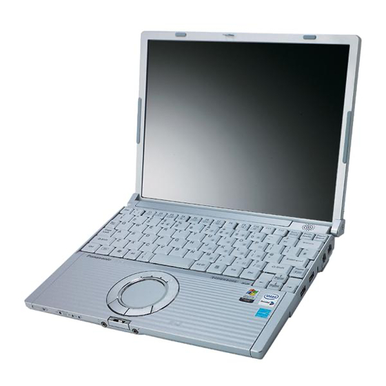
Page 8: Names And Functions Of Parts
2 Names and Functions of Parts A :Function Key G :LCD/Touchscreen B :Keyboard H :Speaker C :LED Indicator I : LAN Port If the Mini Port Replicator is connected to the computer, : Caps lock connect the LAN cable to the LAN port on the Mini Port : Numeric key (NumLk) Replicator. - Page 9 EXT. A :DC-IN Jack G :Microphone Jack B :External Display Port A condenser microphone can be used. If other types If the Mini Port Replicator is connected to the com- of microphones are used, audio input may not be pos- puter, connect the external display to the external dis- sible, or malfunctions may occur as a result.
-
Page 10: Block Diagram
3 Block Diagram... -
Page 11: Diagnosis Procedure
4 Diagnosis Procedure 4.1. Basic Procedures... - Page 12 4.2. Troubleshooting Please take note of the following two points with regard to troubleshooting: 1. Know-how of diagnosis upon occurrence of heavy troubles, e.g. Set cannot be turned ON , Set fails to start , No display on screen , etc. 2.
-
Page 13: Power-On Self Test (Boot Check)
5 Power-On Self Test (Boot Check) Outline of POST The set has a boot check function called POST (Power-On Self Test) in it. The condition of the main body is diagnosed by checking beep sound or error code. Start .....Test begins automatically when power switch is set to ON. Normal finish ..After memory checking, a beep sound is issued once and the set is placed into automatic stop. -
Page 14: List Of Error Codes
If your system displays one of except the messages marked below with an asterisk (*), write down the message and contact Panasonic Technical Support. If your system fails after you make changes in the Setup menus, reset the computer, enter Setup and install Setup defaults or correct the error. - Page 15 02D0 System cache error - Cache disabled Contact Panasonic Technical Support. 02F0: CPU ID: CPU socket number for Multi-Processor error. 02F4: EISA CMOS not writable ServerBIOS2 test error: Cannot write to EISA CMOS. 02F5: DMA Test Failed ServerBIOS2 test error: Cannot write to extended DMA (Direct Memory Access) registers.
-
Page 16: Self Diagnosis Test
The power supply of the computer is turned on. " F2 " is pushed on the screen of "Panasonic" while " press <F2 to enter Setup> " is displayed. The setup utility starts and then takes notes of the content of the BIOS setup of present set. - Page 17 2. Operation of PC-Diagnostic Utility -Only the device which can be inspected on the entire screen is displayed. -The item does not appear when the device of wireless LAN etc. is not physically connected. -The movement of the item must use an arrow key or a flat pad. -As for the device under the diagnosis, blue and yellow are alternately displayed at the left of the icon.
- Page 18 2-3. The content of the setup is returned to the setting of the user Turned on the computer. "F2" is pushed on the screen while "Press<F2>to enter Setup" is displayed of "Panasonic". Push "F10", and on the screen of "Is the change in the setting preserved and do end?"and then "Yes"...
- Page 19 7.1. Test Item and Division of trouble Place with possibili- Test item Stanard Enhancing Content of standard test Content of enhancing test ty of breakdown CPU / CPU is shifted to protected mode, and CPU / SYSTEM "Violation of the paging", "Operation of Main board the violation of a privileged instruc- tion", and DMA, INT, TIMER, and the...
- Page 20 The place with possibility of Test Item Standard Enhanced Content of Standard Test Content of Extend Test breakdown It is confirmed not to find Perform Touch Screen abnormality in the USB functionality practically. Main board/ Touch Screen connection of Touch Screen. Operator has to judge Touch Screen This test cannot find...
-
Page 21: Wiring Connection Diagram
8 Wiring Connection Diagram Connection Cable Connection by Cable LCD Cable DFJS1050ZA Direct connection Connectors SP Cable DFJS962ZA Antenna PCB-L N1ZYYY000002 Parts on Bottom Side Antenna PCB-R N1ZYYY000003 MODEM Cable DFJS973ZB LAN Cable DFJS958ZB PAD FFC DFJK12U112BB FPC Unit,HDD DL3UP1443AAA DC-IN Cable DFJS1020YA USB Cable... -
Page 22: Disassembly/Reassembly
9 Disassembly instructions 9.1. Disassembly Flow Chart Main Unit 9.2.1. Preparation 1. End the Windows. 2. Turn off the Power, and then remove the AC Adaptor or Battery Pack. 3. Remove any optional DIMM Memory Cards or PCMCIA Cards. 4. Remove any other peripherals or Connected Devices. 9.2.2. - Page 23 9.1. Disassembly lnstructions 9.2.1. Preparation Attention: 4. Remove the 6 hooks (B). Before disassembly, be sure to perform the 5. Open the keyboard from LCD side and then turn it following steps. inside out on the top case. 1. End the Windows. Note: 2.
- Page 24 9.2.4. Removing the Top Case 9.2.3. Removing the HDD Preparation : perform the section 9.2.1.,9.2.2. Preparation : perform the section 9.2.1., 9.2.2. first. first. 1. Remove the 7 screws (D) and screws (E). 1. Remove the 2 screws (C) and then remove the Screw (D) : DXHM0039ZA (N5) HDD cover.
- Page 25 9.2.5. Removing the Touch Pad 5. Lift up the top case and remove the pad FFC and then remove the top case. Preparation : perform the section 9.2.1., 9.2.2. and 9.2.4. first. 1. Peel off the tape. Tape : DFHP7140ZA (K37) Top Case 2.
- Page 26 9.2.6. Removing the LCD Knob and the 9.2.8. Removing the Main Board Speaker Preparation : perform the section 9.2.1., 9.2.2. Preparation : perform the section 9.2.1., 9.2.2. and 9.2.4. first. and 9.2.4. first. 1. Remove the 1 screw (I ), 1 screw (J), 2 screws (K) 1.
- Page 27 9.2.9. Removing the Antenna 6.Remove the LCD cable connectors (CN10,CN11). Board (L,R) and the DC-IN Cable Preparation : perform the section 9.2.1., 9.2.2., 9.2.4. and 9.2.8. first. 1. Remove the antenna cable (L) from the main terminal and the antenna cable (R) from the AUX LCD Cable terminal and then remove the antenna board (L, R) from the bottom case.
- Page 28 9.2.11. Removing the MODEM 2.Turn to the card bus ejector side. Preparation : perform the section 9.2.1., 9.2.2., 9.2.4. and 9.2.8. first. 3. Remove the 2 hooks (G) from the connector 1. Remove the 2 screws (O). (CN14). Screw (O) : DXQT2+D25FNL (N8) Card Bus Ejector 2.
- Page 29 9.2.14. Removing the Hinge Cover 9.2.15. Removing the LCD Unit and the LCD Rear Preparation : perform the section 9.2.1., 9.2.2., Preparation : perform the section 9.2.1., 9.2.2., 9.2.4. and 9.2.13. first. 1. Remove the 2 screws (R) and then remove the 9.2.4.
- Page 30 9.2.18. Removing the WWAN Board / LCD 9.2.17. Removing the WWAN Antenna Hook WAN Board (MAIN), (SUB) Preparation : perform the section 9.2.1., 9.2.2., Preparation : perform the section 9.2.1., 9.2.2., 9.2.4. and 9.2.13. to 9.2.15., 9.2.17. first. 9.2.4. and 9.2.13. to 9.2.15. first. 1.
- Page 31 9.3. Reassenbly instructions 9.3.1. Attention when CF-T5L series is repaired - Please execute writing BIOS ID when you exchange the main board. - Parts (sheet and rubber) etc.related various the conductive cloth and heat spreader cannot be recycled.Use new parts. 9.3.2.
- Page 32 9.3.2.3. Putting TP Flexible Protection Tape Sub-materials tape 30mm TP Flexible cable protection tape Upper : Near in the under putting of tape. Upper : The tape is matched to the edge Do not get on and do not go up. of the glass.
- Page 33 9.3.2.5. Assembly of the LCD Unit LCD FRONT Lower and affix FRONT in parallel. Sub-materials tape 30mm The glass LCD resin frame edge side match The other side bottom match Do not go out to the back. LCD unit LCD resin frame The edge of the difference is matched.
- Page 34 Affixation side wall affixation The magnet is applied. LCD DAMPER A It is affixed along the shape of the MAGNET. LCD DAMPER A wall affixation wall affixation 9.3.2.7. Connecting LCD Cable The LCD cable is connected with the inverter. Wraps around the PET tape connector. The inverter is inserted in the inverter box and then affixes to rear case.
- Page 35 ICD / Inverter Cable Connection Safety Work The flaking off paper is peeled off and then affixes on the connector. pressurizes by the finger. 9.3.2.8. Assembly of the Inverter and Putting Inverter Tapes A two sided tape of the Inverter Case bottom is peeled off, and put. Plinth externals standard Safety Work Inverter Case is arranged in the dotted line part.
- Page 36 Safety work Inverter Tape Affixes along shape Do not suppress the tab Safety work Rib root application Affixes along shape From the rib edge Safety work When INVTAPE is affixed on the LCD reception desk rib side, the treatment device is used. 9.3.2.9.
- Page 37 A red line of the cable is matched to the LCD frame externals 9.3.2.10. Putting PET Tape Two sided tape pressurizing The upper part of the LCD resin frame is matched. TP Flexible cable is bent once and the line is processed. Does not hang to the connector on LCD.
- Page 38 9.3.2.11. Line processing LCD cable (2) Sheet edge match After LCD Sheet is turned over and Conductive Cloth is put, a two sided tape is put. Safety work Conductive cloth All the signal lines are processed the conductive cloth internally. Connector Externals edge match Connector and conductive cloth wrapping part,...
- Page 39 The cable is prevented from The tape is distributed at the Safety work coming in succession mutually. center and pasting applying. Safety work The cable is prevented from running aground on the cushion. Put on the hinge surely. LCD Damper C The remainder is put on the hinge side.
- Page 40 PET Tape Conductive Cloth (LCD Cable) The line is processed according to the LVDS cable. LCD insulator is matched to the edge. LCD Cable LCD Cable (Inverter part) Touch panels come most below. Damper Moreover, the LCD cable comes. LCD FRONT wall application affixation. FRAME externals are matched.
- Page 41 Pen Holder Holder Bottom Sheet Arranges match to the rib in the back of Pen Holder. Affixeson Holder Bottom Sheet. LCD Rear side standard The hole of the tape is matched (Convex of the hinge part is disregarded) to the hollow of the insertion part of the pen.
- Page 42 9.3.2.14. Putting LCD Rear Cushions LCD REAR CUSHION LCD REAR CUSHION LCD REAR WAN 9.3.2.15. Assembly of the WM Cable Connector flat side Conductive cloth is wrapped. Black seat edge standard Black seat edge standard 3-7mm from Conductive cloth Filn Impedor is wrapped Film Impedr WM CABLE Finished...
- Page 43 9.3.2.16. Assembly of the WWAN Board LCD Hook Wan installation standard LCD Hook WAN The oreder of tightening screw (LCD Hook WAN) : REAR wall application The oreder of tightening screw (WWAN Board) : There is no order specification Screw excluding a specified part.
- Page 44 A two sided tape of the cable after the cable position A two sided tape of the cable after the cable position of Figure 1 is put out is affixed (cable fixation). of Figure 1 is put out is affixed (cable fixation). The cable must not stretch.
- Page 45 Cable drawing out route Engages with LCD FRONT Refer to Figure 1 goods which have prepared LCD REAR The fingernail in four places is inserted PANASONIC LABEL PANASONIC LABEL Refer to Figure 2 Refer to Figure 2 ANTENNA COVER Safety work...
- Page 46 9.3.2.20. Putting Productive Film Front panel 0.2mm or more The space between the front panel 0.2mm or more and the touch panel surface is based on 0.8-1.2mm 0.2mm or more Productive Film 0.2mm or more Under Do not view from the front in the viewing angle of the right and left 45 Do not view from the front in the viewing angle of the right and left 45 after affixing the film, and no stripe in the surface of the protection film after affixing the film, and no stripe in the surface of the protection film...
- Page 47 9.3.3. Assembly knowhow of the Main Board 9.3.3.1. Putting tapes for Memory Sheet of top side Top side memory Sheet Bond neatly for the memory heat radiation purpose material Safety work It is confirmed that top side memo- ry Sheet does not run aground on the switch.
- Page 48 9.3.3.3. Putting PET tapes The order of tightening screw : Screw : DXQT2+D25FNL Cable’s root is surely suppressed Processes on the capacitor Processes next to the connector Screw A Tape Connector connection Processes to the CHIP set Processes between capacitors (CHIPSETDAI(Dotted line part) Thing that running aground is Affixes between DAI...
- Page 49 9.3.3.4. Assembly of the PCMCIA Ejector (Attention) Affixation load of affixation thing not instructed : More than 1kgf/c Main Board Screw Refer to < Explanation 1 > for the installation. The back of substrate The lever is drawn to The lever is drawn to the Card Bus Ejector the right before building in.
- Page 50 9.3.3.6. Line processing LAN cable Thing to process modem cable previously Thing to process modem cable previously 1.The modem cable is 2.LAN cable afterwards processed to the is processed up bottom ditch part. (Safety work) Affixation load of affixation thing not instructed : More than 1kgf/c Connect the Conector Lithium Battery Connect the Conector...
- Page 51 9.3.3.7. Assembly of the W-LAN Module / Putting Memory Sheet Screw W-LAN DXQT2+D25FNL MODULE (Attention) Affixation load of affixation thing not instructed : More than 1kgf/c Spreads on the terminal BATT (It is one blowing to the range) < Attention > Execute after setting the substrate in the receiving treatment device when working.
- Page 52 9.3.3.8. Putting Sheets (Attention) Affixation load of affixation thing not instructed : More than Pressurize More than 1-1.5 Connector externals application Management size : 0-1mm Grease(G-751) Heat Spreader Bottom Connector externals application Management size : 0-1m Connection Execute after setting the substrate in the receiving treatment device when working.
- Page 53 9.3.3.9. Assembly of the W-LAN Sheet W-LAN Sheet < preparation of W-LAN Sheet > W-LAN Sheet is the sheet W-LAN Sheet metal externals and a difference match. Runs side Horizontal direction is a by side. suiting seat copper part Sheet is lightly held by the finger and the fold externals 0-1mm.
- Page 54 (Attention) Affixation load of affixation thing not instructed : More than 1kgf/c The white line is in respect Mountain case 6mm Valley case 23mm The white line is in respect Use the too Mountain case 35mm Valley case 45mm Use the too Bend completion chart Valley case from white solid line on the back...
- Page 55 9.3.3.11. Assembly of the DC-IN Cable Ferrite Sheet Bends in the vicinity of the connector root. DC-IN Cable It is confirmed to move right and left after wrapping. Bends in the vicinity of the tube root. Safety work Do not give the terminal the load while working.
- Page 56 9.3.4. Assembly knowhow of the Top Case 9.3.4.1. Assembly of the Speaker Soldering of Speaker Cable Affixation of Speaker Ring Solder must not overflow Board externals. Affix and kick according to the shape of the rib. Note not running aground in the rib. Speaker Ring Speaker Soldering...
- Page 57 Safety Work The cable is passed between bosses in the wall and the red circle part. There must not be slack. PET Tape Do not slacken from the tangent which connects the boss externals on the outside. < Speaker Cable processing > 0 2mm(Tape putting standard) Do not slacken from Cab standing wall by 3mm or...
- Page 58 9.3.4.4. Assembly of the LCD Knob Rib match Put on the case before Sheet (Gap 0.5mm or less) inserting the knob Confirm the LCD knob operates after installing the spring. Difference match Spring (Gap 0.5mm or less) KNOB and SRING The spring is hung.
- Page 59 FFC bend specification The gap is 0.5mm or less. MINI-PCI Insert and put a round pin of the Cushion lens on U ditch of the cushion. Bend 0 2mm 0 1mm PET Tape 0 1mm From the tape edge side 180 degree bend From the tape edge side From the tape edge side...
- Page 60 9.3.5. Assembly knowhow of the Bottom Case 9.3.5.1. Setting Antenna Board and Line processing (1) Wiring of Antenna Cable (L) Process Antenna Cable (L) which remained after installing Antenna Board (L) in the Bottom Case as shown in the figure below. Safety work Boss Processes with the boss between ribs...
- Page 61 9.3.5.3. Line processing LAN Cable / USB Cable / MODEM Cable Sheet Put the Sheet to Bottom Rib Sub Board (In the rib edge side match, to the bottom. ) Bottom Rib LAN Cable ANT Cable MODEM Cable Safety work Do not run aground Safety work in the boss.
- Page 62 9.3.6. Assembly knowhow of the Body 9.3.6.1. Setting LCD LCD UNIT SCREW(a) DXQT26+D5FNL SCREW(b) DXQT26+D5FNL Safety work Conductive Cloth is wrapped. 9.3.6.2. Line processing LCD Cable (bottom case side) Work is executed in order of (1) (2) (3) (4). TP Cable Fix Sheet The final state 60 3mm TP Cable Fix Sheet...
- Page 63 Safety work The TP cable must not run aground in the boss. TP cable Connector connection Safety work The tape is pasted from the upper The TP cable is fixed by drawing surface of DC Jack Holder to the line processing Sheet in the direction side and the TP Cable is fixed.
- Page 64 9.3.6.4. Putting Line Hold Sheet WWAN Lower flaking off paper is taken beforehand, and Line Hold Sheet WWAN is pasted to the relay cable according to remaining flaking off paper. Afterwards, Sheet is arranged in Bottom Case. Line Hold Sheet WWAN Safety work is inserted in space in the interior of the Bottom Case.
- Page 65 9.3.6.6. Assembly of the Keyboard Heat Sheet’s KB (largeness) affixation Heat Sheet KB(largeness) Keyboard Edge side match of keyboard hole Inclination 0.5mm or less Inclination 0.5mm or less Edge side match of keyboard hole KB Plate / KB Plate Sheet /Tape affixation KB Plate assembly 2.Both sides tape affixation Tape...
- Page 66 9.3.6.7. Assembly of the Heat Spreader and Side Cover R A remaining tape is affixed on an opposite side Grease (G-751) is spread Safety work (Note) PET Tape When the part of aluminum with a thin all surroundings bends, Sheet and the cable might be damaged.Therefore, correct when bending.
- Page 67 The fingernail is multiplied. Suppresses and installs the direction of the arrow after the connector part is inserted . DDR2 MicroDIMM Screw A (XSB2+4FNL) is tightened. DIMM Cover Screw A 9.3.6.10. The tightening screw of Bottom Case The Keyboard is inserted and after tightening of the Screw, the Keyboard Hook are inserted in order of the following. 1.7 Screws A (DXHM0039ZA) are tightened.
- Page 68 9.3.6.11. Putting Sheets Affixed to the concave part (Exist in the concave part) Bottom Sheet USA The label floatage and the bubble are prevented from being. Pasting applying standard Space of 5mm in surroundings Bottom Backup Sheet Pasting according to the corner Product number : T1207Z Product number : T1206Z Bottom Sheet USA1...
- Page 69 Bottom Case Left justify Left justify Power Knob LAN SW Knob CF-T5*C**** is not used 9.3.6.13. Putting RJ Cover and Labels RJ Cover Safety work RJ Cover is put on the denting part. The paste is prevented from protruding beyond the edge side.
- Page 70 Bottom Sheet USA COA Label The COA label matches and puts externals of Bottom Sheet. Laminate seal The lamination seal sets the direction of Microsoft of polo gram character in the direction of the character of the label. Bottom Sheet USA1 Model Label Revision Label 9.3.6.14.
- Page 71 9.3.6.15. Putting HDD Cover Heat Sheet and Bottom Heat Sheet The left end and the top are set to the concave part of the cover and Bottom Heat Sheet puts Label according HDD Cover Heat Sheet is put. HDD Cover Heat Sheet to a right edge and the top.
- Page 72 9.3.6.16. Putting Tapes for WWAN Antenna Cable After the module is tested, the following work is executed. SCREW Line Hold Sheet The point part of the cable is fixed. (DFHE5025XA) However do not paste the tape on the connector. SCREW (DFHE5025XA) 9.3.6.17.
- Page 73 9.3.6.18. Assembly of the WWAN Module Safety work Edge Guard Tape is put on the point of 1mm on the edge of the module land. Hide the side of the shield board in the module after the Edge Guard Tape putting. Edge Guard Tape is put.
-
Page 74: Exploded View
10 Exploded View 10.1. Display Section K1035 K1038 K1028 E1023 K1026 K1030 E1025 E1026 K1003 E1027 K1030 K1015 K1050 K1051 K1029 N1002 K1048 K1049 K1015 S1001 K1005 K1022 E1024 N1002 K1005 K13 K1052 K1005 K1014 K1018 E1010 K1005 K1016 N1001 K1014 Screw tightening torque K1017... - Page 75 10.2. LCD Unit Ass’y / Pen Holder Section K1024 K1004 K1025 K1019 K1011 E1010 E1010-1 E1010-1-2 E1010-1-5 E1010-1-1 E1010-1-1-1 E1010-1-2 E1010-1-3 E1010-1-5 E1010-1-4 E1010-2 E1010-1-3 E1010-1-6...
- Page 76 10.3. Cabinet Section K1020 Screw tightening torque...
- Page 77 10.4. Bottom Section Screw tightening torque S1002 K1028 CN601 CN12 K1041 CN28 CN22 CN13 K1041 Tape CN14 K1040 K1023 K1010 K1027 K1053 CN1052 K1043 CN1053 N1003 K1021 K1042 K1039 K1039 K1039-1 K1039-1 K1013 K1036 K1046 K1047 K1031 K1001 K1054 K1002...
-
Page 78: Replacement Parts List
12 Replacement Parts List Note : Important Safety Notice Components identified by mark have special characteristics important for safety. When replacing any of these components, use only manufacturer's specified parts. CF-T5LWETZBM REF. NO and AREA PART NO. DESCRIPTION Q'TY Main Block Unit CR2032/S5Y LITHIUM BATTERY DFJK12U112BB... - Page 79 PAD BUTTON DFBD0180ZB-0 POWER SWITCH KNOB DFBD0182ZA-0 LAN SWITCH KNOB DFBH3041ZA HINGE-L TP DFBH3042ZA HINGE-R TP DFBS0076ZA-0 LCD KNOB T5 WAN1 DFGB0089VB-0 PANASONIC LABEL DFGE0124ZB-0 PAD COVER DFGX0425ZA-0 RJ COVER DFGX0428ZA-0 BATT SHEET(T4) DFHE0215ZA SHEET DFHE0436ZA CLOTH LCD CABLE 1 DFHE0843ZA...
- Page 80 DFKE0772ZA-0 ANTENNA COVER-L DFKE0877ZA-0 HINGE COVER L DFKE0878ZA-0 HINGE COVER R DFQT6342ZA DIMM COVER SHEET T5 DFMY3231ZA DIMM HEAT SHEET DFMY0432ZA DIMM THERMAL SPONGE DFKE0783YA-0 SIDE COVER-R DFKF0274ZA-0 LCD FRONT WAN DFKM0523ZA-0 LCD REAR WAN DFKM8172UA-0 TOP CASE ASSY DFMD1203ZA LCD HOOK WAN DFMD3121ZA MDC PLATE...
- Page 81 K1028 DFHR3E92ZA LINE HOLD SHEET A K1029 DFHR5484ZA CLAMP K1030 DFHR8526ZA CABLE FIXED SHEET K1031 DFKE0815ZA-0 DIMM COVER LIGHT K1035 DFKE0879ZA-0 SIMM COVER WAN K1036 DFKE0884ZA-0 HDD COVER WAN K1038 DFKF0275ZB-0 ANTENNA COVER K1039 DFKF8166XA-0 BOTTOM CASE ASSY K1039-1 DFHG371ZA-1 FOOT RUBBER K1040 DFKH1020ZA-0...
- Page 82 Replacement Parts List Note: Important Safety Notice Components identified by mark have special characteristics important for safety. When replacing any of these components use only manufacturer's specified parts. CF-T5LWETZBM (06-10-27) REF. NO and AREA PART NO. DESCRIPTION Q'TY MAIN PCB F1J0J226A051 CAPACITOR, 6.3V, 22µF C 13...
- Page 83 C 135 C 136 C 137 C 142 C 143 C 144 C 145 C 146 C 147 C 148 C 168 C 169 C 171 C 175 C 177 C 178 C 180 C 182 C 183 C 187 C 188 C 189 C 190...
- Page 84 C 296 C 298 C 305 C 310 C 311 C 313 C 314 C 315 C 316 C 317 C 318 C 319 C 321 C 323 C 326 C 328 C 332 C 347 C 351 C 358 C 364 C 375 C 377...
- Page 85 C 167 C 176 C 206 C 280 C 297 C 303 C 304 C 325 C 339 C 368 C 395 C 441 C 446 C 447 C 668 C 695 CAPACITOR, 25V, 0.01µF C 46 F1G1E103A062 C 151 C 152 C 153 C 154...
- Page 86 C 116 C 117 C 130 C 131 C 132 C 133 C 138 C 139 C 140 C 141 C 172 C 173 C 184 C 186 C 214 C 216 C 301 C 322 C 338 C 346 C 390 C 399 C 606...
- Page 87 C 667 C 683 C 686 C 181 EEFSX0D331ER CAPACITOR, 2V, 330µF C 676 C 698 C 708 C 709 C 210 F1G1H100A544 CAPACITOR, 50V, 10pF C 211 C 212 C 404 C 415 C 416 C 418 C 419 CAPACITOR, 6.3V, 150µF C 223 EEFUD0J151ER...
- Page 88 C 287 C 288 CAPACITOR, 10V, 1µF C 263 F1J1A1050021 CAPACITOR, 6.3V, 0.22µF C 264 F1G0J224A001 C 265 C 333 C 334 C 335 C 336 C 366 C 306 F1G1H1010005 CAPACITOR, 50V, 100pF C 307 C 362 C 363 C 385 C 615 C 664...
- Page 89 CAPACITOR, 50V, 0.01µF C 617 F1H1H103A748 C 627 CAPACITOR, 50V, 220pF C 621 F1G1H221A495 C 648 C 661 C 666 C 672 C 679 C 684 C 685 CAPACITOR, 6.3V, 4.7µF C 624 F1J0J475A009 C 649 C 687 C 718 C 733 C 630 EEFCX0G151R...
- Page 90 B0ADDH000004 DIODE D 601 D 602 D 604 D 10 B3ABB0000164 D 11 D 12 D 13 D 15 B3AKB0000008 D 16 B3ACB0000020 D 21 D 20 B3ABB0000274 D 23 MA2S111-TX DIODE D 619 D 621 D 600 B0JCPD000023 DIODE D 603 D 636 D 605...
- Page 91 IC 10 IC 11 IC 12 IC 13 C0JBZZ000388 IC, CLOCK GENERATOR IC 16 C0CBCBG00008 IC, REGULATOR IC 17 C1DB00001182 IC, LAN CONTROLLER IC 18 C3EBCG000100 IC, EEPROM IC 19 C0CBCBC00137 IC, REGURATOR IC 20 C1CB00002540 IC, TEMPERATURE CENSOR IC IC 21 C0DBZYY00026 IC, USB POWER SW...
- Page 92 J0JHC0000074 INDUCTOR L 26 L 54 L 13 J0JCC0000186 INDUCTOR L 14 L 27 L 28 L 29 L 30 L 31 L 32 L 33 L 17 J0JBC0000072 INDUCTOR, FILTER L 18 L 19 L 21 J0ZZB0000080 IDUCTOR, COMMON MODE FILTER L 22 L 25 DDB5Z024E-L...
- Page 93 B1CFGD000023 TRANSISTOR Q 27 Q 647 Q 654 Q 662 Q 663 Q 666 Q 10 XP0421300L TRANSISTOR Q 36 Q 38 Q 628 Q 631 Q 632 Q 634 Q 635 Q 636 Q 11 B1DHDC000028 TRANSISTOR Q 40 Q 630 Q 633 Q 28...
- Page 94 R 187 R 218 R 235 R 272 R 273 R 392 R 393 R 462 R 479 R 480 R 492 ERJ2GEJ510X RESISTOR, 1/16W, 51Ω RESISTOR, 1/16W, 100Ω R 13 ERJ2GEJ101X R 14 R 65 R 203 R 237 R 332 R 350 R 362...
- Page 95 RESISTOR, 1/16W, 5.6KΩ R 31 ERJ2GEJ562X R 354 R 610 R 614 R 616 R 747 RESISTOR, 1/16W, 221Ω R 37 ERJ2RKF2210X R 39 RESISTOR, 1/16W, 100Ω R 38 ERJ2RKF1000X R 40 R 42 RESISTOR, 1/16W, 200Ω R 41 ERJ2RKF2000X RESISTOR, 1/16W, 10KΩ...
- Page 96 R 372 R 374 R 396 R 402 R 413 R 421 R 422 R 426 R 428 R 437 R 444 R 447 R 448 R 452 R 453 R 484 R 519 R 520 R 521 R 619 R 639 R 644 R 688...
- Page 97 R 119 R 120 R 121 R 122 R 123 R 124 R 125 R 126 R 341 R 636 R 637 R 649 R 650 R 705 R 706 R 716 R 717 R 725 R 726 R 737 R 738 RESISTOR, 1/16W, 0Ω...
- Page 98 R 333 R 346 R 386 R 399 R 406 R 407 R 430 R 431 R 449 R 450 R 458 R 472 R 481 R 485 R 487 R 491 R 501 R 600 R 692 R 703 R 719 R 760 R 761...
- Page 99 R 621 R 623 R 624 R 625 R 664 R 666 R 672 RESISTOR, 1/16W, 1Ω R 166 ERJ3GEYJ1R0V R 167 R 168 R 169 R 245 R 699 R 762 R 769 RESISTOR, 1/16W, 4.7KΩ R 174 ERJ2GEJ472X R 754 RESISTOR, 1/16W, 33Ω...
- Page 100 RESISTOR, 1/16W, 47Ω R 221 ERJ2GEJ470X R 222 R 443 R 473 RESISTOR, 1/16W, 22.6Ω R 229 ERJ2RKF22R6X RESISTOR, 1/16W, 120Ω R 246 ERJ3GEYJ121V RESISTOR, 1/16W, 330KΩ R 255 ERJ2GEJ334X R 280 R 355 RESISTOR, 1/16W, 20KΩ R 258 ERJ2GEJ203X RESISTOR, 1/16W, 10MΩ...
- Page 101 RESISTOR, 1/16W, 100KΩ R 605 ERJ2RHD104X R 613 RESISTOR, 1/16W, 150KΩ R 606 ERJ2RKD154X R 612 RESISTOR, 1W, 330Ω R 615 ERJ1TYJ331U R 617 RESISTOR, 1/16W, 3.3Ω R 618 ERJ3GEYJ3R3V R 628 D1BDR1000002 RESISTOR, 1/8W, 0.1Ω R 626 RL1220SR15F RESISTOR, 1/8W, 0.15Ω R 627 RESISTOR, 1/8W, 0.022Ω...
- Page 102 RESISTOR, 1/16W, 100KΩ R 689 ERJ2RKF1003X R 690 ERJ2RKF1800X RESISTOR, 1/16W, 180Ω R 693 ERJ2RKF1801X RESISTOR, 1/16W, 1.80KΩ RESISTOR, 1/16W, 4.7KΩ R 694 ERJ2RKF4701X R 710 R 695 ERJ2RKF4221X RESISTOR, 1/16W, 4.22KΩ R 700 D1ZZ00000093 RESISTOR, 1W, 1mΩ RESISTOR, 1/16W, 15KΩ R 711 ERJ2RKF1502X R 735...
- Page 103 C 1112 C 1113 CAPACITOR, 25V, 0.022µF C 1110 F1G1E223A062 F1G1E472A062 C 1101 CAPACITOR, 25V, 4700pF C 1102 C 1103 C 1104 CAPACITOR, 50V, 1000pF C 1111 F1G1H102A450 CAPACITOR, 6.3V, 0.22µF C 1114 F1G0J224A001 CAPACITOR, 6.3V, 4.7µF C 1115 F1J0J475A009 CAPACITOR, 6.3V, 10µF C 1116 F1J0J106A024...
- Page 104 CN 1502 K1MY52BA0190 MINI-PCI-EXP CONNECTOR CN 1503 K1NA08E00007 CONNECTOR D 1520 DEDRB081L20 DIODE IC 1520 C0DBAYY00204 IC, DC/DC CONVERTER L 1520 G1C2R7MA0273 INDUCTOR, COIL Q 1520 B1CFGD000023 TRANSISTOR Q 1522 B1DHFD000015 TRANSISTOR Q 1521 B1GBCFNN0042 TRANSISTOR RESISTOR, 1/16W, 100Ω R 1502 ERJ2GEJ101X R 1504 RESISTOR, 1/16W, 0Ω...
Need help?
Do you have a question about the CF-T5 and is the answer not in the manual?
Questions and answers