Table of Contents
Advertisement
Quick Links
www.ti.com
User's Guide
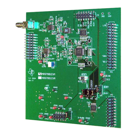
ADS7881EVM, ADS7891EVM Evaluation Module
Lijoy Philipose
This user's guide describes the characteristics, operation, and use of the ADS78x1
12-bit and 14-bit, parallel, analog-to-digital converter (ADC) evaluation module (EVM). Throughout this
document, the terms evaluation board, evaluation module, and EVM are synonymous with the ADS78x1EVM.
A complete circuit description, schematic diagram, layout, and bill of materials (BOM) are included in this
document.
1
Introduction.............................................................................................................................................................................2
1.1 Features.............................................................................................................................................................................
1.2 Analog Interface.................................................................................................................................................................
1.3 Digital Interface..................................................................................................................................................................
1.4 Power Supplies..................................................................................................................................................................
EVM.........................................................................................................................................................................7
Materials...............................................................................................................................................8
Layout............................................................................................................................................................10
5 ADS78x1EVM Schematics...................................................................................................................................................
6 Revision History...................................................................................................................................................................
Figure 1-1. ADS7881 Input Buffer Circuit....................................................................................................................................
Figure 2-1. Decoding Control Signals Using the Address Bus....................................................................................................
Figure 4-3. Power Plane - Layer 3............................................................................................................................................
Figure 4-4. Bottom Layer - Layer 4...........................................................................................................................................
Figure 5-2. Schematic Page 2: ADS7881, ADS7891................................................................................................................
Figure 5-3. Schematic Page 3: Digital Communication.............................................................................................................
Table 1-1. Related Documentation from Texas Instruments........................................................................................................
Table 1-2. Analog Input Connector..............................................................................................................................................
Table 1-4. Pin Out for Parallel Control Connector P2..................................................................................................................
Table 1-5. Jumper Settings..........................................................................................................................................................
Table 1-6. Data Bus Connector P3..............................................................................................................................................
Table 1-7. Pin Out for Converter Control Connector J3...............................................................................................................
Table 1-8. Power-Supply Test Points...........................................................................................................................................
Materials............................................................................................................................................................8
Trademarks
All trademarks are the property of their respective owners.
SLAU150A - DECEMBER 2004 - REVISED OCTOBER 2021
Submit Document Feedback
ABSTRACT
Table of Contents
List of Figures
1.................................................................................................................................................10
2...........................................................................................................................................11
Buffer.............................................................................................................................14
List of Tables
Setting.......................................................................................................................................4
Out.....................................................................................................................................6
Copyright © 2021 Texas Instruments Incorporated
Data Acquisition Products
(ADS7881
and ADS7891)
ADS7881EVM, ADS7891EVM Evaluation Module
Table of Contents
2
2
4
6
14
17
3
7
12
13
15
16
2
2
4
5
5
6
6
1
Advertisement
Table of Contents

Related Manuals for Texas Instruments ADS7881EVM


Summary of Contents for Texas Instruments ADS7881EVM
-
Page 1: Table Of Contents
Buffer..........................14 Figure 5-2. Schematic Page 2: ADS7881, ADS7891........................ Figure 5-3. Schematic Page 3: Digital Communication......................List of Tables Table 1-1. Related Documentation from Texas Instruments......................Table 1-2. Analog Input Connector.............................. Table 1-3. Solder Short Jumper Setting............................4 Table 1-4. Pin Out for Parallel Control Connector P2........................ -
Page 2: Introduction
The following sections describe the pin outs of the various analog, power, and digital connectors and power requirements. Table 1-1 lists documents related to the ADS78x1EVM. Table 1-1. Related Documentation from Texas Instruments Data Sheets Literature Number ADS7881 SLAS400... -
Page 3: Figure 1-1. Ads7881 Input Buffer Circuit
10 kW 1 mF 1000 pF (−)IN 1 mF 0.1 mF 21 W Figure 1-1. ADS7881 Input Buffer Circuit SLAU150A – DECEMBER 2004 – REVISED OCTOBER 2021 ADS7881EVM, ADS7891EVM Evaluation Module Submit Document Feedback Copyright © 2021 Texas Instruments Incorporated... -
Page 4: Digital Interface
The jumper settings allow up to two ADS78x1EVMs to be stacked into processor memory. See Table 1-5 for jumper settings. The evaluation module does not allow the ADS7881EVM, ADS7891EVM Evaluation Module SLAU150A – DECEMBER 2004 – REVISED OCTOBER 2021 Submit Document Feedback Copyright © 2021 Texas Instruments Incorporated... -
Page 5: Table 1-5. Jumper Settings
Not connected Not connected P3.31 Not connected Not connected Not connected All even-numbered pins of P3 are tied to DGND. SLAU150A – DECEMBER 2004 – REVISED OCTOBER 2021 ADS7881EVM, ADS7891EVM Evaluation Module Submit Document Feedback Copyright © 2021 Texas Instruments Incorporated... -
Page 6: Power Supplies
Table 1-9. Power Connector, J1, Pin Out Signal Power Connector - J1 Signal +VA (+12VA) –VA (–12VA) +AVCC (+5VA) AGND +3.3VD +5VD ADS7881EVM, ADS7891EVM Evaluation Module SLAU150A – DECEMBER 2004 – REVISED OCTOBER 2021 Submit Document Feedback Copyright © 2021 Texas Instruments Incorporated... -
Page 7: Using The Evm
P3 and control via J3. SN74AHC138 CONVST DC_CS RESET Figure 2-1. Decoding Control Signals Using the Address Bus SLAU150A – DECEMBER 2004 – REVISED OCTOBER 2021 ADS7881EVM, ADS7891EVM Evaluation Module Submit Document Feedback Copyright © 2021 Texas Instruments Incorporated... -
Page 8: Ads78X1Evm Bill Of Materials
100 MHz, low-noise, high-speed amplifier REF3040, 50 ppm/–C, 50-A in SOT23-3 CMOS 3-SOT-23 Not installed Not installed voltage reference ADS7881EVM, ADS7891EVM Evaluation Module SLAU150A – DECEMBER 2004 – REVISED OCTOBER 2021 Submit Document Feedback Copyright © 2021 Texas Instruments Incorporated... - Page 9 TP5 TP7 TP2 TP13 test_point2 Keystone Electronics 5001K-ND Test point, PC, mini 0.040" D, black Used for the ADS7891EVM only. SLAU150A – DECEMBER 2004 – REVISED OCTOBER 2021 ADS7881EVM, ADS7891EVM Evaluation Module Submit Document Feedback Copyright © 2021 Texas Instruments Incorporated...
-
Page 10: Ads78X1Evm Layout
4 ADS78x1EVM Layout Figure 4-1 Figure 4-4 illustrate the silkscreens for the ADS78x1EVM. Figure 4-1. Top Layer – Layer 1 ADS7881EVM, ADS7891EVM Evaluation Module SLAU150A – DECEMBER 2004 – REVISED OCTOBER 2021 Submit Document Feedback Copyright © 2021 Texas Instruments Incorporated... -
Page 11: Figure 4-2. Ground Plane - Layer 2
ADS78x1EVM Layout Figure 4-2. Ground Plane – Layer 2 SLAU150A – DECEMBER 2004 – REVISED OCTOBER 2021 ADS7881EVM, ADS7891EVM Evaluation Module Submit Document Feedback Copyright © 2021 Texas Instruments Incorporated... -
Page 12: Figure 4-3. Power Plane - Layer 3
ADS78x1EVM Layout www.ti.com Figure 4-3. Power Plane – Layer 3 ADS7881EVM, ADS7891EVM Evaluation Module SLAU150A – DECEMBER 2004 – REVISED OCTOBER 2021 Submit Document Feedback Copyright © 2021 Texas Instruments Incorporated... -
Page 13: Figure 4-4. Bottom Layer - Layer 4
ADS78x1EVM Layout Figure 4-4. Bottom Layer – Layer 4 SLAU150A – DECEMBER 2004 – REVISED OCTOBER 2021 ADS7881EVM, ADS7891EVM Evaluation Module Submit Document Feedback Copyright © 2021 Texas Instruments Incorporated... -
Page 14: Ads78X1Evm Schematics
Data Bus CONVST BYTE PWN/RST A_PWD B_BUSY ADC Control DC_CS INTc Parallel Control Figure 5-1. Schematic Page 1: Digital Buffer ADS7881EVM, ADS7891EVM Evaluation Module SLAU150A – DECEMBER 2004 – REVISED OCTOBER 2021 Submit Document Feedback Copyright © 2021 Texas Instruments Incorporated... -
Page 15: Figure 5-2. Schematic Page 2: Ads7881, Ads7891
R13 =10 Ohm C16 = 1500 pF C0G U4 : ADS7891 130pF Figure 5-2. Schematic Page 2: ADS7881, ADS7891 SLAU150A – DECEMBER 2004 – REVISED OCTOBER 2021 ADS7881EVM, ADS7891EVM Evaluation Module Submit Document Feedback Copyright © 2021 Texas Instruments Incorporated... -
Page 16: Figure 5-3. Schematic Page 3: Digital Communication
B_DB13 0.1uF +VBD INTc SN74AHC245PWR 0.1uF SN74AHC1G04DBV +VBD +VBD SN74AHC138PWR DC_CS DC_CS Figure 5-3. Schematic Page 3: Digital Communication ADS7881EVM, ADS7891EVM Evaluation Module SLAU150A – DECEMBER 2004 – REVISED OCTOBER 2021 Submit Document Feedback Copyright © 2021 Texas Instruments Incorporated... -
Page 17: Revision History
Revision History 6 Revision History Changes from Revision * (December 2004) to Revision A (October 2021) Page • Changed document title from ADS7881/ADS7891EVM to ADS7881EVM, ADS7891EVM Evaluation Module • Changed ADS7881/ADS7891EVM to ADS78x1EVM throughout document............1 • Added Related Documentation from Texas Instruments table to Introduction section........ - Page 18 STANDARD TERMS FOR EVALUATION MODULES Delivery: TI delivers TI evaluation boards, kits, or modules, including any accompanying demonstration software, components, and/or documentation which may be provided together or separately (collectively, an “EVM” or “EVMs”) to the User (“User”) in accordance with the terms set forth herein.
- Page 19 www.ti.com Regulatory Notices: 3.1 United States 3.1.1 Notice applicable to EVMs not FCC-Approved: FCC NOTICE: This kit is designed to allow product developers to evaluate electronic components, circuitry, or software associated with the kit to determine whether to incorporate such items in a finished product and software developers to write software applications for use with the end product.
- Page 20 www.ti.com Concernant les EVMs avec antennes détachables Conformément à la réglementation d'Industrie Canada, le présent émetteur radio peut fonctionner avec une antenne d'un type et d'un gain maximal (ou inférieur) approuvé pour l'émetteur par Industrie Canada. Dans le but de réduire les risques de brouillage radioélectrique à...
- Page 21 www.ti.com EVM Use Restrictions and Warnings: 4.1 EVMS ARE NOT FOR USE IN FUNCTIONAL SAFETY AND/OR SAFETY CRITICAL EVALUATIONS, INCLUDING BUT NOT LIMITED TO EVALUATIONS OF LIFE SUPPORT APPLICATIONS. 4.2 User must read and apply the user guide and other available documentation provided by TI regarding the EVM prior to handling or using the EVM, including without limitation any warning or restriction notices.
- Page 22 Notwithstanding the foregoing, any judgment may be enforced in any United States or foreign court, and TI may seek injunctive relief in any United States or foreign court. Mailing Address: Texas Instruments, Post Office Box 655303, Dallas, Texas 75265 Copyright © 2019, Texas Instruments Incorporated...
- Page 23 TI products. TI’s provision of these resources does not expand or otherwise alter TI’s applicable warranties or warranty disclaimers for TI products.IMPORTANT NOTICE Mailing Address: Texas Instruments, Post Office Box 655303, Dallas, Texas 75265 Copyright © 2021, Texas Instruments Incorporated...
Need help?
Do you have a question about the ADS7881EVM and is the answer not in the manual?
Questions and answers