Table of Contents
Advertisement
Advertisement
Table of Contents

Related Manuals for Icom IC-2720


Summary of Contents for Icom IC-2720
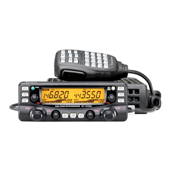
- Page 1 SERVICE MANUAL DUAL BAND FM TRANSCEIVER i2720H...
- Page 2 INTRODUCTION DANGER This service manual describes the latest service information NEVER connect the transceiver to an AC outlet or to a DC for the IC-2720H DUAL BAND FM TRANSCEIVER at the power supply that uses more than 16 V. This will ruin the transceiver.
-
Page 3: Table Of Contents
TABLE OF CONTENTS SECTION 1 SPECIFICATIONS SECTION 2 INSIDE VIEWS SECTION 3 DISASSEMBLY INSTRUCTIONS SECTION 4 CIRCUIT DESCRIPTION 4 - 1 RECEIVER CIRCUITS ............4 - 1 4 - 2 TRANSMITTER CIRCUITS . - Page 4 SECTION 1 SPECIFICATIONS GENERAL • Frequency range LEFT SIDE VERSION RX (MHz) TX (MHz) [KOR] 144.000–146.000, 430.000–440.000 144.000–146.000, 430.000–440.000 [SEA] 136.000–179.995* , 430.000–440.000 140.000–150.000* , 430.000–440.000 [EXP] 118.000–549.995* 136.000–174.000* , 400.000–479.000* [USA] 118.000–549.995* 144.000–148.000, 430.000–450.000* RIGHT SIDE VERSION RX (MHz) TX (MHz) [KOR] 144.000–146.000, 430.000–440.000...
- Page 5 SECTION 2 INSIDE VIEWS • CONTROL UNIT (TOP VIEW) Key back light Key back light LCD back light LCD back light Key back light Key back light (DS14, DS15: LN1371G) (DS14, DS15: LN1371G) DS1-3, DS7-9: SML-010MT DS1-3, DS7-9: SML-010MT (DS16, DS17: LN1371G) (DS16, DS17: LN1371G) DS4-6, DS10-12: SML-020MLT DS4-6, DS10-12: SML-020MLT...
- Page 6 • CONTROL UNIT (BOTTOM VIEW) Dimmer Dimmer circuit Sub CPU Control unit CPU +5V regurator +5V regurator (IC4: HD6473847RH) (IC4: HD6473847RH) (IC3: TA78L05F) (IC3: TA78L05F) (Q6-Q13: 2SC4116) Mic amplifier Mic amplifier Data comparator Data comparator Reset IC Reset IC (IC2: S-80945CLMC) (IC2: S-80945CLMC) IC5: TA75S558F IC5: TA75S558F...
- Page 7 SECTION 3 DISASSEMBLY INSTRUCTIONS Unscrew 2 screws I. • Removing the MAIN unit Unscrew 8 screws A, and remove the cover. Unscrew 12 screws J, and remove MAIN unit. Disconnect two cables B from J1 and J2007. Remove the clip c. MAIN UNIT J2007 Unsolder 3 points E.
- Page 8 • Removing the CONTROL unit Remove 6 knobs A. Unscrew 4 screws B, and remove the cover. Remove the plate C, and remove CONTROL unit. CONTROL UNIT 3 - 2...
-
Page 9: Receiver Circuits
SECTION 4 CIRCUIT DESCRIPTION 4-1 RECEIVER CIRCUITS • RF SIGNALS V220 (174 MHz–260 MHz), V-U1 (225 MHz–375 MHz) 4-1-1 TRIPLEXER AND RX BAND SWITCHING The V220 and V-U1 RF signals from the antenna connector CIRCUITS (MAIN UNIT) are applied to the RX band swtiching circuit (Q34, D66, RL1), The transceiver has a triplexer (low-pass and high-pass fil- and are applied to the left side displayed RX circuit. - Page 10 The signals from the RX band swtiching circuits are then • FM MODE applied to the left side displayed 1st mixer circuit (IC1005, pin The 2nd IF signal is output from the FM IF IC (IC1001, pin 3) and passes through the ceramic bandpass filter (FI1001). The filtered signal is fed back to the IC, and amplified at the limiter amplifier section (pin 5), then demodulated into AF sig- 4-1-3 1ST MIXER AND 1ST IF CIRCUIT FOR LEFT...
- Page 11 A portion of the AF signals from the FM IF IC (IC1001, pin 9) • RF SIGNALS V-U2 (375 MHz–550 MHz) are applied to the active filter section (IC1001, pin 8). The The amplified signals are applied to the RF amplifier (Q19) active filter section amplifies and filters noise components.
- Page 12 The 46.05 MHz 1st IF signal from the IF amplifier (Q1041) is The electronic volume control circuit controls AF gain, there- applied to the 2nd mixer section of the FM IF IC (IC1004, pin fore, the AF output level is according to the [VOL] setting and 16), and is mixed with the 2nd LO signal (45.595 MHz) to be also the squelch conditions.
-
Page 13: Transmitter Circuits
4-2 TRANSMITTER CIRCUITS The “MOD” signal from the D/A convertor IC (IC1009, pin 11) changes the reactance of D5 (VCO unit) to modulate the 4-2-1 MICROPHONE AMPLIFIER CIRCUIT oscillated signal at the VHF-VCO circuit (VCO unit; Q6). The (MAIN AND CONTROL UNITS) modulated signal is amplified at the buffer amplifiers (VCO The microphone amplifier circuit amplifies audio signals from unit;... -
Page 14: Pll Circuits
4-2-5 APC CIRCUIT (MAIN UNIT) • FROM THE VHF-VCO CIRCUIT An oscillated signal from the VHF-VCO circuit (Q1038, The APC circuit protects the pre-drive (Q21), drive amplifier D1014, D1015) passes through the buffer amplifiers (Q1043, (Q25) and power amplifier (Q27) from a mismatched output Q1016) and VCO switch (D1023) is applied to the PLL IC for load and stabilizes the output power. - Page 15 • UHF-VCO 4-3-4 PLL CIRCUIT FOR LEFT SIDE DISPLAY The oscillated signal at the UHF-VCO circuit is amplified at (VCO UNIT) the buffer amplifiers (Q1044, Q1047), and is then applied to An oscillated signal from the L-VCO circuit passes through the VCO switch (D2059, D2060) to divide UHF TX signal the buffer amplifiers (Q7, Q1) is applied to the PLL IC for left and RX signal.
-
Page 16: Power Supply Circuits
4-4 POWER SUPPLY CIRCUITS (1) NORMAL OSCILLATING SIGNAL CIRCUIT The signal from the VCO swtich (D7) passes through the 4-4-1 CONTROL UNIT VOLTAGE LINE attenuator (R33, R37, R38, C41) and low-pass filter (L5, L9, Description Line C45, C47, C53, C63, C64), and then applied to the VCO swtich (D10) which is controlled by the “L_VR5”... - Page 17 4-4-2 MAIN UNIT VOLTAGE LINE MAIN UNIT VOLTAGE LINE–Continued Line Description Line Description The 13.8V external DC power from the power Receive 5 V produced from the 5VS line at the connector. R_AM5 regulator circuit (Q3). The output voltage L220_R5 is applied to the RF amplifier (Q31) for left side The same voltage as the HV line which is con- display’s 220 MHz bandpass filter.
- Page 18 4-5 PORT ALLOCATIONS 4-5-1 CPU (MAIN UNIT; IC2013) Port Port Description Description number name number name FAN_CTRL Outputs microphone mute signal for Outputs cooling fan control signal. UMMUTE right side display. CLONE_OUT Outputs the cloing data signal. Low: While microphone is muting. CLONE_IN Input port for the cloing data signal.
- Page 19 CPU-Continued 4-5-2 D/A CONVERTER IC (CONTROL UNIT; IC4) Port Port Description Description number name number name Outputs shift signal to the 430 MHz R_BPF3 Output tracking signals to the band- 2, 3 bandpass filter for left side display. R_BPF4 pass filter for right side display. L_400SHIFT High:While receiving 310–450 MHz L_BPF1,...
-
Page 20: Parts List
SECTION 5 PARTS LIST [CONTROL UNIT] [CONTROL UNIT] ORDER ORDER DESCRIPTION DESCRIPTION 1110002750 S.IC TA75S01F (TE85R) 7030003440 S.RESISTOR ERJ3GEYJ 102 V (1 kΩ) 1110005780 S.IC S-80945CLMC-G7F-T2 7030003440 S.RESISTOR ERJ3GEYJ 102 V (1 kΩ) ERJ3GEYJ 391 V (390 Ω) 1180000420 S.IC TA78L05F (TE12R) 7030003390 S.RESISTOR 1140010230 S.IC... -
Page 21: Main Unit
[CONTROL UNIT] [MAIN UNIT] ORDER ORDER DESCRIPTION DESCRIPTION 4550000530 S.TANTALUM TESVA 1V 104M1-8L 1110004310 S.IC M62352GP 75EC 4550005980 S.TANTALUM TEMSVA 1A 475M-8L 1110002750 S.IC TA75S01F (TE85R) 4550003220 S.TANTALUM TEMSVA 1E 105M-8L IC1000 1110005340 S.IC NJM12902V-TE1 4550006250 S.TANTALUM TEMSVA 1A 106M-8L IC1001 1110003200 S.IC TA31136FN (EL) IC1003 1130004200 S.IC... - Page 22 [MAIN UNIT] [MAIN UNIT] ORDER ORDER DESCRIPTION DESCRIPTION Q1021 1530002690 S.TRANSISTOR 2SC4116-GR (TE85R) 1750000710 S.VARICAP HVC350BTRF Q1022 1590001190 S.TRANSISTOR XP6501-(TX) .AB 1750000510 S.DIODE UM9401F Q1023 1530002850 S.TRANSISTOR 2SC4116-BL (TE85R) 1790000980 S.DIODE MA742 (TX) Q1025 1590001190 S.TRANSISTOR XP6501-(TX) .AB 1790001240 S.DIODE MA2S728-(TX) Q1026 1590001650 S.TRANSISTOR XP4601 (TX) 1720000240 S.DIODE...
- Page 23 [MAIN UNIT] [MAIN UNIT] ORDER ORDER DESCRIPTION DESCRIPTION D2063 1790001620 S.DIODE 1SV308 (TPL3) 6200005670 S.COIL ELJRE 12NG-F D2064 1790001620 S.DIODE 1SV308 (TPL3) 6200005670 S.COIL ELJRE 12NG-F D2065 1790001620 S.DIODE 1SV308 (TPL3) 6200005740 S.COIL ELJRE 47NG-F D2066 1790001620 S.DIODE 1SV308 (TPL3) 6200005740 S.COIL ELJRE 47NG-F D2067...
- Page 24 [MAIN UNIT] [MAIN UNIT] ORDER ORDER DESCRIPTION DESCRIPTION ERJ3GEYJ 470 V (47 Ω) 7030003280 S.RESISTOR R133 7030003600 S.RESISTOR ERJ3GEYJ 223 V (22 kΩ) [USA] MCR10EZHJ 47 Ω (470) 7030000220 S.RESISTOR 7030003520 S.RESISTOR ERJ3GEYJ 472 V (4.7 kΩ) [OTHER] ERJ3GEYJ 330 V (33 Ω) 7030003260 S.RESISTOR R134 7030003680 S.RESISTOR...
- Page 25 [MAIN UNIT] [MAIN UNIT] ORDER ORDER DESCRIPTION DESCRIPTION R1030 7030003530 S.RESISTOR ERJ3GEYJ 562 V (5.6 kΩ) R1129 7030003560 S.RESISTOR ERJ3GEYJ 103 V (10 kΩ) R1031 7030003580 S.RESISTOR ERJ3GEYJ 153 V (15 kΩ) R1131 7030003590 S.RESISTOR ERJ3GEYJ 183 V (18 kΩ) R1032 7030003580 S.RESISTOR ERJ3GEYJ 153 V (15 kΩ)
- Page 26 [MAIN UNIT] [MAIN UNIT] ORDER ORDER DESCRIPTION DESCRIPTION R1285 7030003470 S.RESISTOR ERJ3GEYJ 182 V (1.8 kΩ) R2101 7030003640 S.RESISTOR ERJ3GEYJ 473 V (47 kΩ) R1286 7030003510 S.RESISTOR ERJ3GEYJ 392 V (3.9 kΩ) R2102 7030003520 S.RESISTOR ERJ3GEYJ 472 V (4.7 kΩ) R1288 7030003640 S.RESISTOR ERJ3GEYJ 473 V (47 kΩ)
- Page 27 [MAIN UNIT] [MAIN UNIT] ORDER ORDER DESCRIPTION DESCRIPTION R2236 7030003520 S.RESISTOR ERJ3GEYJ 472 V (4.7 kΩ) 4030006900 S.CERAMIC C1608 JB 1H 103K-T R2237 7030003760 S.RESISTOR ERJ3GEYJ 474 V (470 kΩ) 4030006990 S.CERAMIC C1608 CH 1H 080D-T R2238 7030003680 S.RESISTOR ERJ3GEYJ 104 V (100 kΩ) 4030006990 S.CERAMIC C1608 CH 1H 080D-T R2239...
- Page 28 [MAIN UNIT] [MAIN UNIT] ORDER ORDER DESCRIPTION DESCRIPTION C162 4030006860 S.CERAMIC C1608 JB 1H 102K-T C265 4030011730 S.CERAMIC GRM31M2C2H101JV01L C163 4030006860 S.CERAMIC C1608 JB 1H 102K-T C266 4030006920 S.CERAMIC C1608 CH 1H 010C-T C164 4030006860 S.CERAMIC C1608 JB 1H 102K-T C267 4030006920 S.CERAMIC C1608 CH 1H 010C-T...
- Page 29 [MAIN UNIT] [MAIN UNIT] ORDER ORDER DESCRIPTION DESCRIPTION C1062 4550003220 S.TANTALUM TEMSVA 1E 105M-8L C1195 4030006860 S.CERAMIC C1608 JB 1H 102K-T C1063 4030006860 S.CERAMIC C1608 JB 1H 102K-T C1197 4030006900 S.CERAMIC C1608 JB 1H 103K-T C1065 4030006900 S.CERAMIC C1608 JB 1H 103K-T C1198 4030006900 S.CERAMIC C1608 JB 1H 103K-T...
- Page 30 [MAIN UNIT] [MAIN UNIT] ORDER ORDER DESCRIPTION DESCRIPTION C2037 4030006860 S.CERAMIC C1608 JB 1H 102K-T C2132 4030006860 S.CERAMIC C1608 JB 1H 102K-T C2038 4510006240 S.ELECTROLYTIC ECEV1CA221P C2133 4030017200 S.CERAMIC GRM31BR32J102KY01L C2039 4510006260 S.ELECTROLYTIC ECEV1AA471UP C2134 4030006860 S.CERAMIC C1608 JB 1H 102K-T C2040 4510006220 S.ELECTROLYTIC ECEV1CA101UP C2135...
-
Page 31: Vco Unit
[MAIN UNIT] [VCO UNIT] ORDER ORDER DESCRIPTION DESCRIPTION 6510014960 S.CONNECTOR B2B-ZR-SM3-TF 1140005990 S.IC MB15A02PFV1-G-BND-ER J2001 6510023110 CONNECTOR 3008L-8P8C 1130004200 S.IC TC4S66F (TE85R) J2003 6510023160 CONNECTOR DN-508B-6 1110004460 S.IC µPB1509GV-E1 J2004 6450002220 CONNECTOR PJ-0008P-5 J2005 6450001440 CONNECTOR HSJ1403-01-010 J2006 6510023170 CONNECTOR 3008L-6P6C 1530002560 S.TRANSISTOR 2SC4403-3-TL J2007... - Page 32 [VCO UNIT] [VCO UNIT] ORDER ORDER DESCRIPTION DESCRIPTION 7030003640 S.RESISTOR ERJ3GEYJ 473 V (47 kΩ) 4030007020 S.CERAMIC C1608 CH 1H 120J-T 7030003440 S.RESISTOR ERJ3GEYJ 102 V (1 kΩ) 4030007030 S.CERAMIC C1608 CH 1H 150J-T 7030003520 S.RESISTOR ERJ3GEYJ 472 V (4.7 kΩ) 4030007040 S.CERAMIC C1608 CH 1H 180J-T 7030003560 S.RESISTOR...
- Page 33 SECTION 6 MECHANICAL PARTS AND DISASSEMBLY [CHASSIS PARTS] [MAIN UNIT] REF. ORDER REF. ORDER DESCRIPTION QTY. DESCRIPTION QTY. 6510004880 Connector MR-DS-E 01 J2001 6510023110 Connector 3008L-8P8C J2003 6510023160 Connector DN-508B-6 2510001160 Speaker 057P0802 J2004 6450002220 Connector PJ-0008P-5 J2005 6450001440 Connector HSJ1403-01-010 2710000730 Fan AD0412HB-G70 (TS) J2006...
- Page 34 MP9 (C) MP11 (C) J1 (C) MP2 (CT) MP1 (C) MP11 (CT) MP10 (CT) MP4 (C) MP11 (CT) R1 (CT) MF1 (C) J2 (CT) MP3 (CT) MP13 (CT) S1 (CT) J2004 (M) MP9 (CT) J2005 (M) R3 (CT) MP13 (C) MP12 (C) EP15 (CT) W2 (M)
- Page 35 SECTION 7 SEMI-CONDUCTOR INFORMATION • TRANSSISTORS AND FET’S • DIODES 2SA1586 GR 2SA1588 GR 2SB1132 T100 R 2SC4116 BL 2SC4116 GR 1SS355 1SV172 1SV308 DA221 TL DAN222TL (Symbol: SG) (Symbol: ZG) (Symbol: BAR) (Symbol: LL) (Symbol: LG) (Symbol: A) (Symbol: BE) (Symbol: TX) (Symbol: K) (Symbol: N)
- Page 36 SECTION 8 BOARD LAYOUTS 8-1 CONTROL UNIT • TOP VIEW MAIN MAIN BAND BAND V/MHz V/MHz SCAN SCAN M/CALL M/CALL TONE MONI DTMF PRIO DIAL DIAL TDATA MICU/D RDATA EXTMIC MICE MICE MICIN to MAIN unit J2006 to Microphone 8 - 1...
- Page 37 • BOTTOM VIEW (CONTROL UNIT) 8 - 2...
- Page 38 8-2 MAIN UNIT • TOP VIEW J2007 to Speaker to VCO unit J5 to VCO unit J2 L_VCO_SHIFT CHASSIS OUT4 REF_MOD L_PLLSW L_VCO8 L_UNLOCK L_TXLO to VCO unit J3 CHASSIS J2000 to FAN 8 - 3...
- Page 39 • BOTTOM VIEW (MAIN UNIT) J2003 DATAOUT PSQL DATAIN PTTP AFOUT to external equipment J2001 MICIN MICE EXTMIC MICU/D to Microphone J2006 CTHV TXDATA RDATA MICE to CONTROL unit J2 8 - 4...
- Page 40 8-3 VCO UNIT • TOP VIEW 8 - 5...
- Page 41 • BOTTOM VIEW (VCO UNIT) to MAIN unit L_TXLO L_VCO8 OUT4 L_VCO_SHIFT to MAIN unit to MAIN unit to MAIN unit to MAIN unit 8 - 6...
-
Page 42: Block Diagram
SECTION 9 BLOCK DIAGRAM DATAMOD MODIN L300 L400 L140 L220 J2001 IC1009 IC1000C MICU/D M62363FP-650C Q2022,Q2023 IC2008 NJM12902V EXTMIC DTC144EU BU4066BCFV L UR5 L VR5 Q1012 Q1009 BUFF 2SC4116 2SC4215 2nd_LO_38.4MHz MIC_SENS BUFF BUFF MICE D1040 D1041 Q1023 SENS IC2007 IC1000A IC1000D DAN222... - Page 43 VUT8 ANTENNA T UHF D42 UM9401F (430-450MHz) D46 UM9957 D2070,D36 D57,D61 D67 MA2S077 D70 MA8047 2SK3075 D52,D2049 MA2S111 RD70HVF1 UM9401F MA742 D71 MA742 R_UVCO_SEL 450kHz DRIVE TX/RX BUFF DRIVE FI1000 FI1001 CFWM450E CFWS450HT R_RVCO_SEL D77,D78 CERAMIC CERAMIC 1SV308 2SC4226 2SK2854 2SK3475 Q1013 DTA144EU L140...
-
Page 44: Voltage Diagrams
SECTION 10 VOLTAGE DIAGRAMS 10-1 CONTROL UNIT CONTROL UNIT DS19 L1-0500TAM DS10 SML-020MLT SML-020MLT EVQ-VENF02 L.DIUD L.DICK DS11 SML-020MLT SML-020MLT XP4601 EVQ-VENF02 R.DIUD R.DICK DS12 SML-020MLT SML-020MLT 4.7k L.VOL SEG34 SEG8 P91/SEG34 P57/WKP7/SEG8 SEG35 SEG7 P92/SEG35 P56/WKP6/SEG7 SEG36 SEG6 P93/SEG36 P55/WKP5/SEG6 R54 1k SEG37... -
Page 45: Main And Vco Units
10-2 MAIN AND VCO UNITS MAIN UNIT(1) 13.7V WN_SEL BUS LINE1 BUS LINE2 J2000 W2001 IC2003 TA7808F R2000 Q2000 2SB1132 13.77V IC2012 C2044 R2077 LA4445 D2032 D2036 D2040 D2044 MATORIX_IN1 C2042 R2076 IC2002 Q2002 D2033 D2037 D2041 D2045 TA7805F R2105 2SA1588 NTCG20 R2161... - Page 46 MAIN UNIT(2) BUS LINE1 BUS LINE1 BUS LINE1 BUS LINE1 BUS LINE2 BUS LINE2 BUS LINE2 BUS LINE2 R1005 R1009 3.9k VCO UNIT DTCS IC1009 C1023 RX: 7.11V R1045 M62363FP-650C 1SV308 1SV308 220k VIN1 VIN8 L_VCO8 L VCO8 0.001 VOUT1 VOUT8 Q1001 R1288...
- Page 47 MAIN UNIT(3) BUS LINE1 BUS LINE1 BUS LINE2 BUS LINE2 BUS LINE2 BUS LINE2 R2210 C1207 TX: 0V 0.001 RX: 0V R1173 R1158 8.2k 1.2k C1289 R_VVCO_SEL R1135 R1139 R1116 4.7k R1159 R1169 R1236 8.2k 1.2k R_UVCO_SEL 4.7k C1304 C1173 R1204 Q1026 XP4601...
- Page 48 MAIN UNIT (4) BUS LINE2 BUS LINE2 VHF TX: 7.83V 7.92V RX: 0V 2SA1588 C293 220p R2216 R2218 C287 DTC144EU 0.001 8.2n 0.001 C73 100p VTX_CTRL TX: 6.07V 2SA1588 1SV308 RX: 0V 0.001 DTC144EU 2SK3475 C2183 C2184 2SK2854 UTX_CTRL 1SV308 470p 470p HF50ACC322513-B...
- Page 49 MAIN UNIT (5) CHASSIS BUS LINE2 BUS LINE2 L140_R5 L140_R5 ATQ209 C129 C2137 RX: 2.73V 0.5p 0.001 C153 L1048 C2138 3SK272 C112 RX: 3.72V MA2S077 2SC4116 V-V(118-180MHz) C165 C202 R149 R2192 L_BPF4 L_BPF4 0.5p 0.001 L_BPF3 L_BPF3 C2136 C158 100p VATT R142 L_BPF2...
- Page 51 S-13907HZ-C1 1-1-32, Kamiminami, Hirano-ku, Osaka 547-0003, Japan © 2002 Icom Inc.
Need help?
Do you have a question about the IC-2720 and is the answer not in the manual?
Questions and answers