Sign In
Upload
Download
Add to my manuals
Delete from my manuals
Share
URL of this page:
HTML Link:
Bookmark this page
Add
Manual will be automatically added to "My Manuals"
Print this page
×
Bookmark added
×
Added to my manuals
Manuals
Brands
Panasonic Manuals
Cordless Telephone
KX-TCD430FXB
Service manual
Panasonic KX-TCD430FXB Service Manual
Telephone eguipment
Hide thumbs
1
2
3
4
5
6
7
8
9
10
11
12
13
14
15
16
17
18
19
20
21
22
23
24
25
26
27
28
29
30
31
32
33
34
35
36
37
38
39
40
41
42
43
44
45
46
47
48
49
50
51
52
53
54
55
56
57
58
59
60
61
62
63
64
65
66
67
68
69
70
71
72
73
74
75
76
77
78
79
80
81
82
83
84
85
86
87
88
89
90
91
92
93
94
95
96
97
98
99
100
101
102
103
104
105
106
107
108
109
110
111
112
113
page
of
113
Go
/
113
Bookmarks
Advertisement
Quick Links
Download this manual
ORDER NO. KM40402351C2
Telephone Equipment
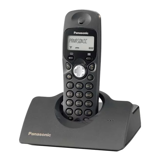
KX-TCD430FXB / KX-TCD430FXC / KX-TCD430FXW / KX-
A143EXB / KX-A143EXC / KX-A143EXW
Digital Cordless Phone
Black Version
Dark Blue Version
White Version
(for Nordic Countries)
SPECIFICATIONS
1
Previous
Page
Next
Page
1
2
3
4
5
Advertisement
Need help?
Do you have a question about the KX-TCD430FXB and is the answer not in the manual?
Ask a question
Questions and answers
Related Manuals for Panasonic KX-TCD430FXB
Cordless Telephone Panasonic KX-TCD430GC Service Manual
Digital cordless phone, dark/light blue version for germany (115 pages)
Cordless Telephone Panasonic KX-TCD430HK Specifications
Dect digital multi-handset clear sound long range (2 pages)
Cordless Telephone Panasonic KX-TCD430AL Operating Instructions Manual
Panasonic digital cordless phone operating instructions (32 pages)
Cordless Telephone Panasonic KX-TCD430NZ Operating Instructions Manual
Digital cordless phone (32 pages)
Cordless Telephone PANASONIC KX-TCD430E Operating Instructions Manual
Digital cordless phone (32 pages)
Cordless Telephone Panasonic KX-TCD440NZ Operating Instructions Manual
Digital cordless phone digital cordless answering system (40 pages)
Cordless Telephone Panasonic KX-TCD410NZ Operating Instructions Manual
Digital cordless phone (40 pages)
Cordless Telephone PANASONIC KX-TCD440E Operating Instructions Manual
Digital cordless phone and digital cordless answering system (40 pages)
Cordless Telephone PANASONIC KX-TCD400E Operating Instructions Manual
Digital cordless phone (32 pages)
Cordless Telephone Panasonic KX-TCD410AXM Service Manual
(115 pages)
Cordless Telephone Panasonic KX-TCD400RUB Service Manual
Telephone equipment (81 pages)
Cordless Telephone Panasonic KX-A144 Series Service Manual
(93 pages)
Cordless Telephone Panasonic KX-TCD400GC Service Manual
(99 pages)
Cordless Telephone Panasonic KX-TCD410ALM Service Manual
Digital cordless phone metallic grey version silver version (for australia) (110 pages)
Cordless Telephone Panasonic KX-TCD410SLS Service Manual
(106 pages)
Cordless Telephone Panasonic KX-TCD400HGB Service Manual
Black/dark blue version for hungary (84 pages)
This manual is also suitable for:
Kx-tcd430fxc
Kx-tcd430fxw
Kx-a143exb
Kx-a143exc
Kx-a143exw
Print
Rename the bookmark
Delete bookmark?
Delete from my manuals?
Login
Sign In
OR
Sign in with Facebook
Sign in with Google
Upload manual
Upload from disk
Upload from URL


Need help?
Do you have a question about the KX-TCD430FXB and is the answer not in the manual?
Questions and answers