
Related Manuals for Nordic Semiconductor nRF51822


Summary of Contents for Nordic Semiconductor nRF51822
- Page 1 Development Kit nRF51822 User Guide v1.4 Copyright © 2013 Nordic Semiconductor ASA. All rights reserved. Reproduction in whole or in part is prohibited without the prior written permission of the copyright holder.
-
Page 2: Table Of Contents
Development Kit User Guide v1.4 Contents Introduction............................... 3 Minimum requirements ..........................3 External resources ............................3 Writing conventions............................3 Development Kit release notes ........................3 Kit content..............................4 nRF51422 Development Kit hardware content..................4 Downloadable content ..........................5 Quick start ..............................6 Install the nRF51422 connector module.................... -
Page 3: Introduction
The nRF51822 Development Kit (DK) for Bluetooth® low energy/2.4 GHz proprietary provides a complete solution for developing, testing, and evaluating the nRF51822 device. nRF51822 is part of the nRF51 series which offers a range of ultra-low power System on Chip (SoC) solutions for your 2.4 GHz wireless products. -
Page 4: Kit Content
Development Kit User Guide v1.4 Kit content The nRF51822 DK consists of hardware and access to software components, documentation, and design files from www.nordicsemi.com. nRF51822 Development Kit hardware content 1 x Helical monopole SMA antenna 5 x nRF51822 chip samples... -
Page 5: Downloadable Content
• nRF51 SDK • nRF51822 PAN 2.2.3 Schematics, Bill of Materials, PCB layout files, and production files The ZIP file and its subdirectories contain the hardware design files for the nRF51822 DK. • Altium Designer files • Schematics • PCB layout files •... -
Page 6: Quick Start
Development Kit User Guide v1.4 Quick start This section shows you how to set up the nRF51822 Development Kit and provides example applications to help you start programming your device. Register, download, and install 1. If you have Keil MDK-ARM Lite already installed, go to step 2. Otherwise, download and install Keil MDK-ARM Lite from https://www.keil.com/demo/eval/arm.htm... -
Page 7: Install The Nrf51422 Connector Module
Install the nRF51822 connector module Connect the hardware 1. Screw the antenna into the SMA connector on the nRF51822 DK SMA (PCA10005) connector module. 2. Ensure that header K1 has a jumper connecting pin 2 and 3. The two upper rows of P4 should have two jumpers placed vertically matching the 32 kHz marking. - Page 8 Motherboard. Make sure the red marking on the cable is always connected to pin 1, as shown in the figure below. 6. Connect the SEGGER J-Link board to the nRF51822 module with the 10 pin flat cable (1.27 mm, provided in the Development Kit).
- Page 9 Development Kit User Guide v1.4 Turn on and set the supply voltage 1. Slide the S8 switch on the Motherboard to VBUS. 2. Slide the On/Off switch on the Motherboard to ON. 3. The VCC and VTG LEDs will light up.
- Page 10 5. Select the desired motherboard from the Device Manager pane in nRFgo Studio. To find the board ID, look on the 7-segment display on the Motherboard. 6. In nRFgo Studio, you can control the supply voltage (VTG) to the connected nRF51822 module. Make sure the voltage is set to 3.3 V.
- Page 11 \ARM\Device\Nordic\nRF51822\Board\nrf6310\blinky_example\arm. 2. Open the Blinky project in Keil μVision by double clicking the blinky.uvproj file. 3. Select nRF51822 from the Select Target list and click Build or press F7 to compile the Blinky project. 4. Click the Load icon to download and run the Blinky example firmware. LED0 to LED7 on the nRFgo Starter Kit Motherboard should now blink sequentially.
- Page 12 Development Kit User Guide v1.4 Bluetooth low energy heart rate monitor demo This section shows you how to program a heart rate monitor demo on top of a SoftDevice that will send data on a Bluetooth link from the heart rate monitor to the Master Control Panel.
- Page 13 4. Only one SEGGER device should be connected to your computer. Make sure it is also connected to the nRF51822 development module to ensure the program is downloaded to the correct target. 5. Go to the Flash menu and click Download to load the program (or click the Load icon).
- Page 14 Development Kit User Guide v1.4 8. Click Enable services. You should see the Heart Rate Measurement characteristic and Battery Level being notified every few seconds with a different value (the Heart Rate Measurement/ Battery Level value line will blink green for each notification).
-
Page 15: Development Kit Configuration
Development environment setup The nRF51822 device can be programmed from several environments. This section shows the development setup using Keil MDK-ARM. The nRF51822 DK can be configured to develop proprietary 2.4 GHz protocol- based applications and Bluetooth 4.0 single-mode applications. - Page 16 Keil nRF51 SDK Keil µVision IDE SAMSUNG J-Link Lite Application Programming & Erase (Via J-Link) nRFgo Studio 10 pin Flat Cable Configure Voltage nRF51822 module Figure 2 nRF51822 DK configuration for 2.4 GHz based development Page 16 of 62...
- Page 17 Master Control Panel Control Keil µVision IDE SAMSUNG PCA10000 J-Link Lite Application Programming & Erase (Via J-Link) nRFgo Studio 10 pin Flat Cable Configure Voltage nRF51822 module Figure 3 nRF51822 DK configuration for Bluetooth 4.0 single-mode Page 17 of 62...
-
Page 18: Kit Setup
Development Kit User Guide v1.4 Kit setup USB connected to computer nRF51 module 10 pin 2.54 mm flat cable 10 pin 1.27 mm flat cable J-Link Lite CortexM USB connected to computer Figure 4 Kit setup Page 18 of 62... - Page 19 The nRF51822 Development Dongle (PCA10000) enables you to see the data sent between the dongle and a single nRF51822 device. The nRF51822 Development Dongle is plugged into a USB port on your computer as described in “Compile, program, and run the heart rate monitor demo“ on page 13.
- Page 20 Development Kit User Guide v1.4 Connect the JTAG/SWD emulator using the 10 pin 1.27 mm flat cable supplied with the kit to the nRF51822 DK module at P3 and to your computer with a USB cable, as shown in Figure 6.
-
Page 21: Hardware Description
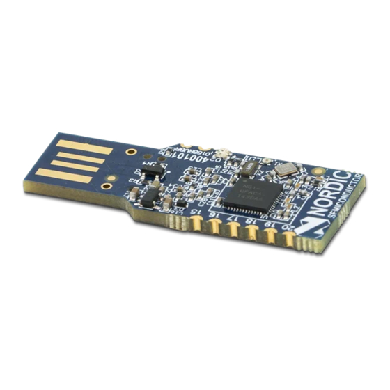
Development Kit User Guide v1.4 Hardware description This chapter describes the nRF51822 DK modules and the nRF51822 Development Dongle (PCA10000). nRFgo nRF51822 DK modules The nRF51822 modules (PCA10004, PCA10005) are delivered with an unprogrammed nRF51822 chip. 5.1.1 Key features The nRF51822 DK modules have the following key features: •... - Page 22 Development Kit User Guide v1.4 5.1.2 Hardware pictures Figure 7 nRF51822 DK module (PCA10004) top Figure 8 nRF51822 DK module (PCA10004) bottom Page 22 of 62...
- Page 23 Development Kit User Guide v1.4 Figure 9 nRF51822 DK module (PCA10005) top Figure 10 nRF51822 DK module (PCA10005) bottom Page 23 of 62...
- Page 24 Development Kit User Guide v1.4 5.1.3 Block diagram Ext A1 Ext B1 SMA/ Matching Analog nRF51822 network antenna 32.768 kHz 16 MHz Figure 11 nRF51822 DK module block diagram Page 24 of 62...
- Page 25 Development Kit User Guide v1.4 5.1.4 nRFgo nRF51822 DK module extension Connectors P1 and P2 on the nRF51822 DK module connect to the Motherboard. VCC_nRF' VCC_nRF' P0.00 P0.01 P0.24 P0.25 P0.02 P0.03 P0.26 P0.27 P0.04 P0.05 P0.28 P0.29 P0.06 P0.07...
- Page 26 5.1.5 Analog inputs Direct access to the nRF51822 analog input is available on connector P5 on the nRF51822 DK module. Note: P5 is not mounted on the board. The analog inputs are routed through the extension connectors to the Motherboard. To avoid noise from ...
- Page 27 Development Kit User Guide v1.4 5.1.6 SWD interface The programming and debugging interface is accessed through the 10 pin connector P3 on the nRF51822 DK module. SWDIO SWDCLK Figure 14 SWD interface connector P3 Label Description Reference voltage for programmer...
- Page 28 On the nRF51822 DK module, P0.26 and P0.27 are disconnected from the Motherboard and connected to the two jumpers on the nRF51822 DK module at the position 32 kHz on connector P4 (Pin 1 and Pin 3 for XL1 and Pin 2 and Pin 4 for XL2). This is the default position of the jumpers when shipped.
- Page 29 For current measurements using the CSM, the jumper on connector K1 must be placed on Pin 2 and Pin 3. This is the default position of the jumpers when shipped. Current on the nRF51822 module is measured on connector K2 as voltage proportional to the current.
- Page 30 COM port provided by the SEGGER chip. The PCA10000 can be loaded with Master Emulator firmware, that when combined with the Master Control Panel, gives you a peer device for nRF51822 that you can use to test the wireless connection.
- Page 31 Figure 19 PCA10000 block diagram Figure 20 5.2.4 Mulitcolor LED The Development Dongle (PCA10000) is equipped with a multicolor RGB LED. The LED is connected to dedicated I/Os on the nRF51822 chip. The connections are shown in Table 3. Color GPIO P0.21 Green P0.22...
- Page 32 Note: The UART signals are routed directly to the SEGGER chip. The pins should only be used for UART. In order to use the USB to UART bridge, the software on the nRF51822 has to enable flow control. For details on how to set up the UART with flow control, see the nRF51 Series Reference Manual.
-
Page 33: Flash Programming And Application Development
The nRF51822 chip is shipped without pre-programmed software. This gives you the option of developing your application directly onto the chip or alternatively, by using our S110 nRF51822 SoftDevice, which is a Bluetooth low energy peripheral protocol stack solution. For more information, see the S110 nRF51822 SoftDevice Specification. - Page 34 6.1.2 Identifying the nRF51 chip and chip content When you select a board, nRFgo Studio identifies the nRF51822 chip and how its memory is organized. The following chip and memory information is displayed: • nRF51 chip identification - Identifies the chip by name and code variant (for example, nRF51822 QFAACA).
- Page 35 4. Set the SoftDevice size. This sets the size of the code memory region 0 and will not be available if the size is defined by the HEX file. Note: The S110 nRF51822 SoftDevice can be downloaded from www.nordicsemi.com by logging into your MyPage account and entering the product key printed in the Development Kit.
- Page 36 Development Kit User Guide v1.4 6.1.5 Programming an application This function lets you program an application onto the chip. Before nRFgo Studio starts programming it verifies that the HEX file matches the actual memory configuration. If it matches, nRFgo Studio continues with the programming, if not it stops the programming and returns an error message.
-
Page 37: Application Development
0x2000 Table 6 SoftDevice memory layout Note: See the nRF51822 Product Specification for details on the total code memory and RAM available in the device. The amount of code memory and RAM used by the SoftDevice is described in the S110 nRF51822 SoftDevice Specification. - Page 38 Development Kit User Guide v1.4 6.2.1.1 Memory layout configuration in Keil IDE To access the Keil IDE memory layout: 1. Click the Project menu and select Options for Target. 2. Select the Linker tab. 3. Check Use memory layout from Target Dialog.
- Page 39 Development Kit User Guide v1.4 4. Select the Target tab. 5. In Read/Only Memory Areas, define values for Start and Size. 6. In Read/Write Memory Areas, define values for Start and Size as seen in Figure 24. 7. Click OK.
- Page 40 Development Kit User Guide v1.4 6.2.2 Shared call stack The user application shares the call stack with the SoftDevice if the SoftDevice is loaded on the chip. The application must reserve enough memory for both itself and the SoftDevice in the call stack. The call stack size required by the SoftDevice varies between devices and protocol stack versions, and is supplied in the S110 nRF51822 SoftDevice Specification.
- Page 41 Development Kit User Guide v1.4 6.2.3 Debugger configuration Project files delivered in the SDK are configured and ready for download and debugging. If a new application project is used, the debugger must be properly configured. To configure the debugger: 1.
- Page 42 Development Kit User Guide v1.4 7. In the Target driver setup, provide information about debugging protocol and maximum speed. Select SW in the Port drop-down. 8. In Max Clock the maximum speed for the debugging port cannot be exceeded (1 MHz). A proper configuration is shown in Figure 26.
- Page 43 Memory Protection Unit implements a write protection to certain peripherals used by the protocol stack. Protected peripherals are described in the S110 nRF51822 SoftDevice Specification.Configure the debugger and compile and link the application code. Download the application using the Keil IDE download button.
- Page 44 Development Kit User Guide v1.4 8. In the Utilities tab, select Use Target Driver for Flash Programming. 9. Choose the available debugger from the list as shown in Figure 29. Figure 29 Debugger selection 6.2.6 Erasing the device The code memory area available for the user application can be erased by doing the following: 1.
-
Page 45: Debugging The Nrf51422
Development Kit User Guide v1.4 Debugging the nRF51822 For debugging with SEGGER J-Link, see Appendix A on page 56. For general information of how to debug using the Keil μVision IDE, see http://www.keil.com/uvision/debug.asp. The following steps tell how to configure the debugger in Keil. -
Page 46: Nrf51422 Debug Features And Precautions
Development Kit User Guide v1.4 nRF51822 debug features and precautions This section contains information about the System Viewer Windows and debugging an application when a readback protected SoftDevice is present. 7.1.1 System Viewer windows The System Viewer enables you to select device peripherals and see their contents in separate windows. In the View menu point to System Viewer and select the peripheral you want to see. - Page 47 Any values in peripheral registers that are restricted or blocked by the SoftDevice will be invisible to the debugger as well. Information on the SoftDevice configuration and memory resource mapping can be found in the S110 nRF51822 SoftDevice Specification. Note: Avoid single stepping to the protected area. Instead, set the breakpoint right after SVC calls while debugging and run the application to the actual breakpoint, see Figure 34 on page 48.
- Page 48 Development Kit User Guide v1.4 Figure 34 Setup with breakpoint after an SVC call Page 48 of 62...
- Page 49 • No parity Kit setup for UART The Direct Test Mode is accessed through the UART on the nRF51822 module. The following steps show how to get set up for DTM testing. 1. Mount one of the nRF51822 modules (either PCA10004 or PCA10005) onto the nRFgo Motherboard.
- Page 50 Development Kit User Guide v1.4 UART J-Link Lite Cortex M Figure 35 UART setup for DTM Page 50 of 62...
- Page 51 Development Kit User Guide v1.4 P2.1 P2.0 Table 8 UART setup The DTM is designed for use with Bluetooth test equipment. If you don't have a Bluetooth tester you can access the interface using this Development Kit and nRFgo Studio to run the tests.
- Page 52 Development Kit User Guide v1.4 Programming the nRF51822 module with DTM The nRF51822 module has to be programmed with the DTM application found in the nRF51 SDK. This application is provided with its source code and needs to be compiled using Keil.
-
Page 53: Software Development Kit
Development Kit User Guide v1.4 Software Development Kit The nRF51 Software Development Kit (SDK) enables you to develop applications for the following protocol stacks: • Bluetooth low energy (using the S110_nRF51822 SoftDevice) • Proprietary 2.4 GHz, including Nordic's Gazell protocol •... -
Page 54: Troubleshooting
The nRF51822 device on the PCA10004/5 does not respond when I try to contact it. What has happened? Verify that the jumper on connector K1 on the nRF51822 module is set in the position Pin 2 and Pin 3. When I connect multiple SEGGER J-Link debugger boards to my computer, μVision does not recognize them correctly. - Page 55 Development Kit User Guide v1.4 The debugger is not able to detect my nRF51 device after I have downloaded my firmware. If the nRF51 device goes to SystemOff too soon after reset, it will have a problem communicating with the J-Link debugger.
-
Page 56: Appendix A: Installing Drivers And Configuring Keil Projects For The Segger Debugger
Development Kit User Guide v1.4 Appendix A: Installing drivers and configuring KEIL projects for the SEGGER debugger This appendix describes the steps for installing the software and using the SEGGER J-Link Lite debugger with Keil μVision for nRF51 series devices, based on J-Link software version 4.52b or later. - Page 57 Development Kit User Guide v1.4 4. Go to http://www.segger.com/IDE_Integration_Keil.html#knownproblems for MDK v4.54. Download JL2CM3 and copy it to <keil>/ARM/Segger. This patch is necessary for the SEGGER debugger to work. 5. Plug in the J-Link Lite CortexM-9 module with USB cable. The LED will blink while the driver installation occurs.
- Page 58 Development Kit User Guide v1.4 Configuring KEIL projects for SEGGER debugger for first time use 1. Double-click an example project file to open the Keil μVision IDE. 2. Click Target Options on the toolbar or click Project menu and select Options for Target Figure 38 Keil Target configuration 3.
- Page 59 Development Kit User Guide v1.4 Note: If the SEGGER J-Link Lite firmware requires an update you will be prompted with the message “A new firmware version is available for the connected emulator”. In this case, click OK. Figure 40 SEGGER control panel 5.
- Page 60 Development Kit User Guide v1.4 6. Select the J-Link device for target programing. Figure 42 Flash settings 7. If the J-Link serial number appears in the SN field, the device is properly installed. The default settings can be accepted by clicking OK, closing both the SEGGER Control Panel and Keil target Driver Setup.
- Page 61 Development Kit User Guide v1.4 Liability disclaimer Nordic Semiconductor ASA reserves the right to make changes without further notice to the product to improve reliability, function or design. Nordic Semiconductor ASA does not assume any liability arising out of the application or use of any product or circuits described herein.
- Page 62 Development Kit User Guide v1.4 Revision history Date Version Description March 2014 Updated content: • Section 3.2 “Bluetooth low energy heart rate monitor demo” on page 12. • Section 8.1 “Kit setup for UART” on page 49. • Section 8.2 “Programming the nRF51822 module with DTM”...
Need help?
Do you have a question about the nRF51822 and is the answer not in the manual?
Questions and answers