Table of Contents
Advertisement
Quick Links
Advertisement
Chapters
Table of Contents
Troubleshooting

Related Manuals for Hytera MD78X


Summary of Contents for Hytera MD78X
- Page 1 SERVICE MANUAL DIGITAL MOBILE RADIO...
- Page 2 To repair the product properly, please read this manual carefully before repairing. This manual is applicable to the following product: MD78X Digital Mobile Radio (X may indicate 2, 5, 6 or 8) MD78XG Digital Mobile Radio (X may indicate 2, 5, 6 or 8) ...
- Page 3 Copyright Information Hytera is the trademark or registered trademark of Hytera Communications Corporation Limited (the Company) in PRC and/or other countries or areas. The Company retains the ownership of its trademarks and product names. All other trademarks and/or product names that may be used in this manual are properties of their respective owners.
- Page 4 Documentation Information Conventions Icon Conventions Icon Description Indicates information that can help you make better use of your product. Note Indicates references that can further describe the related topics. Caution Indicates situations that could cause data loss or equipment damage. Warning Indicates situations that could cause minor personal injury.
- Page 5 UHF1 (400–470 MHz)
-
Page 6: Table Of Contents
UHF1 (400–470 MHz) Contents Contents 1. Product Controls ..........................1 2. Disassembly and Reassembly ......................3 2.1 Disassembling the Radio ........................3 2.2 Reassembling the Radio ........................4 3. Exploded View and Packing Guide ....................5 3.1 Exploded View ..........................5 3.2 Packing Guide .......................... - Page 7 UHF1 (400–470 MHz) Contents 9. PCB View ............................. 55 10. Block Diagram ..........................59 11. Schematic Diagram .......................... 62 12. Parts List ............................76 12.1 Front Panel ........................... 76 12.2 GPS Circuit ........................... 77 12.3 Main Board (25 W) ........................77 12.4 Main Board (45 W) ........................
-
Page 8: Product Controls
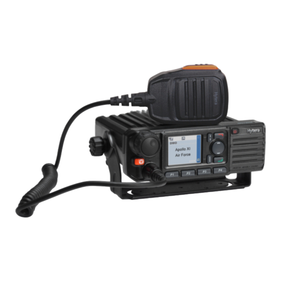
UHF1 (400–470 MHz) Product Controls 1. Product Controls Front Panel Part Name Part Name Volume Control/Group Call Selector Up Key Knob LED Indicator Down Key LCD Display Speaker OK/Menu Key Redial/Answer/Call Key Back/Group Call Management Key Programmable Keys Dial-back/End/Home Screen Key Microphone Connector Power On/Off Key Microphone Installation Index... - Page 9 UHF1 (400–470 MHz) Product Controls Rear Panel Part Name Part Name RF Antenna Connector Accessory Connector Power Inlet GPS Antenna Connector Note The GPS antenna interface is only available for MD78XG.
-
Page 10: Disassembly And Reassembly
UHF1 (400–470 MHz) Disassembly and Reassembly 2. Disassembly and Reassembly Disassembling the Radio Turn off the radio and remove the power cord, and loosen the two screws to remove the radio. Step 1 Remove the antenna. Step 2 Loosen the three screws to remove the front panel. Then remove the FFC. Step 3 Detach the volume control knob and loosen the four screws. -
Page 11: Reassembling The Radio
UHF1 (400–470 MHz) Disassembly and Reassembly Loosen the eleven screws to remove the upper shield cover. Step 6 Loosen the screw fixing the antenna connector and two screws fixing the PA module. Then take Step 7 the PCB out. Reassembling the Radio To reassemble the radio, perform the above steps in a reverse way. -
Page 12: Exploded View And Packing Guide
UHF1 (400–470 MHz) Exploded View and Packing Guide 3. Exploded View and Packing Guide Exploded View Part list: Part No. Description Qty. Part No. Description Qty. 6300109000000 Aluminum chassis 6100334000000 O-ring for encoder switch 7500358000000 Heat sink pad 4399030000020 Rotary switch 6100492101000 Waterproof ring for front 41078001000J0 PCB for control panel... - Page 13 UHF1 (400–470 MHz) Exploded View and Packing Guide Part No. Description Qty. Part No. Description Qty. heat sink pad 4210080000700 Speaker cable (with 2-Pin 3414999000020 PNP transistor plug) 5001210000390 Speaker Main PCB 7400297000000 Speaker felt 6100532100000 D_SUB waterproof ring 7102505000110 Machine screw 5208026100000 Jack 6001076000010 Front case for control...
-
Page 14: Packing Guide
UHF1 (400–470 MHz) Exploded View and Packing Guide Packing Guide... -
Page 15: Specifications And Blind Spot
UHF1 (400–470 MHz) Specifications and Blind Spot 4. Specifications and Blind Spot Specifications General Frequency Range 400–470 MHz Channel Capacity 1024 Group Capacity 64 (each with a maximum of 16 channels) Channel Spacing 12.5 kHz / 20 kHz / 25 kHz Operating Voltage 13.6V±15% DC ... - Page 16 UHF1 (400–470 MHz) Specifications and Blind Spot 12.5 kHz (data and voice): 7K60FXW ±2.5 kHz@12.5 kHz Modulation Limit ±4.0 kHz@20 kHz ±5.0 kHz@25 kHz 40 dB@12.5 kHz FM Hum and Noise 43 dB@20 kHz ...
- Page 17 UHF1 (400–470 MHz) Specifications and Blind Spot 40 dB@12.5 kHz Hum and Noise 43 dB@20 kHz 45 dB@25 kHz Internal (20 Ω load): 3 W Rated Audio Power External (8 Ω load): 7.5 W Internal (20 Ω load): 8 W Max.
-
Page 18: Blind Spot
UHF1 (400–470 MHz) Specifications and Blind Spot Cold Start TTFF (Time To First Fix) <10s Hot Start Horizontal Accuracy <10 m Note All Specifications are tested according to applicable standards, and subject to change without notice due to continuous development. Blind Spot Blind Spot (MHz) Blind Spot (MHz) -
Page 19: Circuit Description
UHF1 (400–470 MHz) Circuit Description 5. Circuit Description Front Panel Front panel includes components such as power supply, keys, LCD, LED indicators, backlight, MMC interface and volume control knob. The function diagram is shown below. CONTROL HEAD Keys Matrix Back Switch Down Menu... - Page 20 UHF1 (400–470 MHz) Circuit Description Conventional Mode Trunking Mode Navigation Key S5 and S11 OK/Menu Key Back/Group Call Management Power On/Off Key Dial-back/End/Home Screen Redial/Answer/Call Key The front panel adopts TFT LCD to transfer data to U302 via the EMIFS data bus. The control signals include read/write enable signal, memory chip select signal, LCD chip select signal and reset signal, each of which is pulled up by R36, R35, R34, R33 and R6 respectively.
-
Page 21: Baseband
UHF1 (400–470 MHz) Circuit Description Baseband 5.2.1 Power Supply Module Auto baterry Voltage Q802\Q803\U201\Q909 13.6±15% Q804\Q805 9V1A 9V3A Q920\Q921\U914 Q810 Q801 9V1A Q6102 Q902 Q6103 U703 U701 3V3A U702 U701 4V3A U915 Q104 Q100\Q103\Q106\Q110 U100 3V3A X100 U918 ON\OFF KEY PWB IGN_SENCE U905 U500... -
Page 22: Control Module
UHF1 (400–470 MHz) Circuit Description Supply for Baseband: The processor U302 is supplied by 3.3 V (U900), 1.8 V (U903) and 1.6 V (U919); the memory (U232/U233) is supplied by 3.3 V (U900) and 1.8 V (U903) respectively; the audio processor IC (U231) is supplied by 3.3 V (U905&U909&U900) and 1.8 V (U903);... - Page 23 UHF1 (400–470 MHz) Circuit Description U917 generates reset signal and remains low level for 1.25 seconds, allowing the processor Step 2 (U302) to get started. Power-on signal is sent to the processor (U302). Step 3 After receiving the signal, the processor (U302) generates the level of PWR_CTRL. Then the Step 4 power-up procedures are completed.
- Page 24 UHF1 (400–470 MHz) Circuit Description MCSI1.CLK U100 U302 DATA MCSI1.DOUT MCSI1.SYNC When U302 is communicating with U100, it works in Master Mode with clock frequency of up to 9.6 MHz. U100 uses MCSI1.CLK as the clock, MCSI1.DOUT as data cable to configure its register, and MCSI1.SYNC as chip select signal.
- Page 25 UHF1 (400–470 MHz) Circuit Description MCBSP3.CLKX PCMCLK MCBSP3.FSX PCMSYNC Option Board MCBSP3.DX PCMIN MCBSP3.DR PCMOUT MCBSP1.CLKX BCLK MCBSP1.FSX WCLK U231 MCBSP1.DX SDIN MCBSP1.DR SDOUT U302 MCBSP2.CLKR CLKOUT U701 MCBSP2.FSR DOUT MCBSP2.DR SCLK MCBSP2.CLKX U500 MCBSP2.FSX MCBSP2.DX U302 provides three MCBSP interfaces including MCBSP1, MCBSP2 and MCBSP3, which are compatible with various interfaces.
- Page 26 UHF1 (400–470 MHz) Circuit Description UART Interface GPS_UART1_TXD U302 UART1.TX GPS_UART1_RXD UART1.RX UART2.TX UART2.TX CONTROLHEAD UART2.RX (GPIO17/GPIO18) UART2.RX UART3_TXD_BT UART3.TX UART_RXD UART3_RXD_BT UART3.RX UART_TXD UART3_RTS_BT Option Board UART3.RTS UART_CTS UART3_CTS_BT UART3.CTS UART_RTS USB_D+ USB_D- Processor U302 provides three UART interfaces, which are used to communicate with different external devices.
- Page 27 UHF1 (400–470 MHz) Circuit Description Option Board Interface J400, an option board interface, is used to achieve specific function by connecting to the designated option board. The definition of each pin is listed as below: Voltage I/O of the Signal Function Remarks...
-
Page 28: Audio Module
UHF1 (400–470 MHz) Circuit Description Voltage I/O of the Signal Function Remarks (Option Board Radio VDD=3.3 V) (standard output from the main AF MB TO OB MAX: 700mV board to the option board) DGND DGND 3V6 or 5V Power Voltage: 5.0 V 5.2.3 Audio Module The audio module is used to output RX audio and input relay audio and TX audio, which serves as the... -
Page 29: Pcb Difference
UHF1 (400–470 MHz) Circuit Description audio signal to the codec (U231), and adjusts the signal to appropriate amplitude according to the volume (RMS should be 80 mV when frequency is 1 kHz and deviation is 3 kHz). Then the codec (U231) converts PCM data into analog audio data via DAC. -
Page 30: Rf Section
UHF1 (400–470 MHz) Circuit Description 3V3D U910 R932 /PRST1 4.7K D913 SENCE 》 /PRST REST MBRM120LT1G C937 1000p C941 0.15u D912 R920 MBRM120LT1G U906 R923 3V3D /RST R983 C978 《 RST_CTRL 0.1u RESETIC The watchdog circuit is used to prevent the mobile radio from damage due to OMAP malfunction. If the program works properly, U302 feeds pulse signal (25 ms) to the watchdog circuit through RST_CTRL. - Page 31 UHF1 (400–470 MHz) Circuit Description Power Amplifier Circuit The power amplifier circuit consists of four-stage power amplifier circuits and amplifies the signal output from VCO to the required output power level. Note Only one final-stage PA (Q803) is available, if the power of the mobile radio is 25 W and the version of main board is Version H or later version.
- Page 32 UHF1 (400–470 MHz) Circuit Description In TX mode TX signal controls the switching transistor Q810, to further control the power supply (9 V 3 A) for the PIN diodes D801 and D802. Quiescent bias current of the PIN diode is controlled by the resistors R821 and R825.
-
Page 33: Receiver Circuit
UHF1 (400–470 MHz) Circuit Description rubber part mounted on the upper cover. When the switch is turned off, the power control voltage VGG will become low, and no power will be output from PA. Otherwise, PA will work normally. 5.3.2 Receiver Circuit The receiver circuit employs double conversion superheterodyne technique. -
Page 34: Fgu Circuit
UHF1 (400–470 MHz) Circuit Description Receiver Back-end GCP GCN MXOP MXON IF2P IF2N 16dB SSI TO OMAP DECIMATION DOUTA FORMATTING/SSI Σ-ΔADC IFIN FILTER DOUTB CLKOUT FREF CONTROL LOGIC VOLTAGE CLK SYN REFERENCE IOUTL CLKN VREFP VCM VREFN IOUTC CLKP PC PD PE SYNCB LO VCO AND LOOP LOOP FILTER... - Page 35 UHF1 (400–470 MHz) Circuit Description Data Registers Clock PD/Charge Pump Serial MSB/LSB Reference Divider & Pwr-Dn/Mux Out Interface Dividend Frequency Dividers Control Mod_in Modulation Mux_out Unit ΔΣ 18-Bit Fractional Reference Unit Frequency Oscillator Main Main Divider Divider Fref_main Fref_main Main Phase/ Freq.Detector Reference Frequency...
-
Page 36: Gps Circuit Section
UHF1 (400–470 MHz) Circuit Description and the other two VCOs (Q106 and Q110) to receive LO signals. U302 controls the operating frequency of the VCO. Q102 and Q107 constitute the buffer amplifiers for the transmitter circuit, while Q111 and Q109 for the receiver circuit. The digital-to-analog converter (U500) modulates the TX oscillator signal. GPS Circuit Section Power Antenna... -
Page 37: Troubleshooting Flow Chart
UHF1 (400–470 MHz) Troubleshooting Flow Chart 6. Troubleshooting Flow Chart Control Circuit Check the control circuit Cannot drive Power-on indication is Verify the the RF circuit normal?[1] control circuit properly Front panel FFC is Replace FFC normal?[2] X302 (19.2 MHz) is U905 (5VA) and Check normal? -
Page 38: Gps Circuit
UHF1 (400–470 MHz) Troubleshooting Flow Chart [4] The output voltage of U905 and U909 is 5 V and 3.3 V respectively. [5] The output voltage of U902 is 5 V. [6] The output voltage of U900 and U901 is 3.3 V. [7] The output voltage of U903 is 1.8 V. -
Page 39: Tx Circuit
UHF1 (400–470 MHz) Troubleshooting Flow Chart [5] R368 and R370 have no soldering defects. TX Circuit Check TX circuit Power supply is Check the power normal? supply circuit Check PA matching Current is normal? circuit, antenna switch, and low-pass circuit, etc Control voltage is Check U801 normal? [2]... -
Page 40: Rx Circuit
UHF1 (400–470 MHz) Troubleshooting Flow Chart [2] The voltage at TP811 is above 2 V. [3] The output amplitude of the TX LO signal at TP803 is about 10 dBm. Make sure that the back-end circuit is disconnected during test. [4] The gain is 16 dB and the input signal is 0 dBm at Q801. - Page 41 UHF1 (400–470 MHz) Troubleshooting Flow Chart Check RX circuit Check the power-on Q920 outputs 9V3A? circuit Check Q902 and Q902 outputs 9V1A? Q903 Replace the front Front panel output is panel normal? [1] Check Q701 and Input an IF signal (73.35 Second LO is normal? peripheral MHz) and test whether the...
-
Page 42: Frequency Generation Unit (Fgu)
UHF1 (400–470 MHz) Troubleshooting Flow Chart [4] The sensitivity at TP6101 is about -110 dBm. [5] The received LO signal at TP6106 is about 18 dBm。 [6] The sensitivity at TP6104 is about -120 dBm. [7] The sensitivity at TP6103 is -117 dBm. Frequency Generation Unit (FGU) Check FGU U915 outputs 5 V and... - Page 43 UHF1 (400–470 MHz) Troubleshooting Flow Chart [3] The emitter voltage of Q106, Q110, Q100 and Q103 is about 1.8 V. [4] The CV of TP124 ranges from 0.5 V to 4.5 V. [5] PLL U100 is supplied by 5 V and 3.3 V normally. [6] The power of the signal from TP109 to PLL is about -15 dBm.
-
Page 44: Interface Definition
UHF1 (400–470 MHz) Interface Definition 7. Interface Definition 10-Pin Connector The 10-pin connector on the front panel is used for audio accessories or data cable connection. The definition of each pin is described as below. Signal Electrical Name Type Description Performance Pin 1 and Pin 10 (accessory identifier interface 2) compose... - Page 45 UHF1 (400–470 MHz) Interface Definition Signal Electrical Name Type Description Performance code is 11. Modulation sensitivity Mic input Analog input Mic input for palm microphone Vrms=80mV±10%@1kHz 60%system max. deviation When this pin is used for USB data USB_D+ USB data function, USB function of DB26 cable+ will be disabled.
-
Page 46: Db26 Accessory Interface
UHF1 (400–470 MHz) Interface Definition Pin 1 Pin 10 Radio Status The mobile radio is connected to an external speaker (including High level Low level desktop microphone with earpiece). The mobile radio is in USB slave mode, or it is not connected to any High level High level accessory, or it is connected to a palm microphone without keypad. - Page 47 UHF1 (400–470 MHz) Interface Definition Signal Electrical Name Type Description Performance Power Power supply :13.2V±15%; Power output: 13.2 V; output SWB+ output output current ≤1 A current: ≤1 A Programmable output Analog (“External Horn & Lights” feature External Alarm voltage 13 V alarm output by default, programmable via output...
- Page 48 UHF1 (400–470 MHz) Interface Definition Signal Electrical Name Type Description Performance three accessory identification statuses. Please refer to the “DB26 Accessory Identification Matrix Table” below for detailed function definitions. Emergency switch. This pin is Emerg Sw Digital input 5V TTL valid when low level is input.
-
Page 49: Other Interfaces
UHF1 (400–470 MHz) Interface Definition Signal Electrical Name Type Description Performance cable Digital GP5_7 5V TTL GPIO. Programmable via CPS. input/output Digital GP5_6 5V TTL GPIO. Programmable via CPS. input/output Load impedance >1 kΩ AUX Audio Out Analog Auxiliary audio (external speaker) output output 1 Vrms=300 mV±10%... - Page 50 UHF1 (400–470 MHz) Interface Definition Pin No. Name Description Grounding pin 2.5–3.3 V adjustable port 2.5–3.3 V adjustable port IOVCC 1.65–3.3 V adjustable I/O port Synchronization signal control port Chip select signal Register select Write signal Read signal Data bus DB10 DB11 DB12...
- Page 51 UHF1 (400–470 MHz) Interface Definition Pin No. Name Description DB16 DB17 RESET Reset signal Select data cable LEDA LED anode LED_K1 LED_K2 LED cathode LED_K3 J4 (Aviation Interface of Front Panel) Pin No. Name Description ACC_IO1 Digital input PTT_IN Digital input External_Audio Analog output USB_D- USB data cable...
- Page 52 UHF1 (400–470 MHz) Interface Definition Voltage I/O of the Pin No. Signal Function Remark (Option Board Radio VDD=3.3 V) VOH MIN=0.8VDD board. GPIO3 VOL MAX=0.22VDD GPIO4/GPIO5: GPIO4 Unidirectional output interfaces. They require their input resistances GPIO5 RESET-OUT greater than equal to 47 kΩ. UART-TX UART-RX UART-CT...
- Page 53 UHF1 (400–470 MHz) Interface Definition Voltage I/O of the Pin No. Signal Function Remark (Option Board Radio VDD=3.3 V) (standard AF MB TO output from the main MAX: 700mV board to the option board) DGND DGND 3V6 or 5V Power Voltage: 5.0 V J403 (Pin Interface) Pin No.
- Page 54 UHF1 (400–470 MHz) Interface Definition Pin No. Name Description Spkr+ Analog output D- USB USB data cable- GP5_8 Input/output Ground Ground cable GP5_7 Input/output GP5_6 Digital input/output AUX Audio Out Analog output AUX Audio Out Analog output Ign Sense Analog voltage input J404 (Front Panel Interface) Pin No.
- Page 55 UHF1 (400–470 MHz) Interface Definition Pin No. Name Description SPKR1- Speaker audio signal cable- Power supply PRST Reset signal KB_C0 KB_C1 KB_C2 KB_C3 Matrix keyboard B_R0 B_R1 B_R2 CSLED Backlight control IC chip select CLOC Backlight control IC clock DATA Backlight control IC data OE_LCD LCD read enable...
- Page 56 UHF1 (400–470 MHz) Interface Definition Pin No. Name Description Grounding PWB_IN Power On/Off signal...
-
Page 57: Tuning Description
UHF1 (400–470 MHz) Tuning Description 8. Tuning Description Required Test Instruments Radio communication test sets: HP8921 and Aeroflex 3920 Power supply: 15 A/30 V Multimeter Tuner software Tuning Procedures 8.2.1 Tuning the Radio After re-assembling the radio, you need to tune it with the Tuner software and HP8921. The specific operations are described in the table below. - Page 58 UHF1 (400–470 MHz) Tuning Description Items Method Click the “Transmit On” button on Tuner. Adjust the power to the required level as follows: Low power: 1 W (for version D/F); 5 W (for version H or later) Medium power: 25 W High power: 45 W Click the “Save”...
- Page 59 UHF1 (400–470 MHz) Tuning Description Items Method Click the “Transmit On” button on Tuner. Then set the modulation signal of HP8921 to “100 Hz”. Adjust the value in the dialog box on Tuner until the frequency deviation displayed on HP8921 is “5 kHz”. Press the Enter key on the keyboard to confirm your settings.
-
Page 60: Testing The Radio
UHF1 (400–470 MHz) Tuning Description Items Method to RX test mode. Set HP8921 to output an unmodulated RF signal with a value of “-70 dBm/Frequency (current channel frequency)”. Press the Enter key on the keyboard to confirm your settings. Click the “Save” button on Tuner to save the existing value to the radio. Connect the radio to HP8921 via the antenna connector, and set HP8921 to RX test mode. - Page 61 UHF1 (400–470 MHz) Tuning Description Magnitude Error: ≤1% UUT TX Bit Err = 0% Click the “Transmit Off” button on Tuner to finish testing. Step 7 Receiving Connect the antenna connector of the radio to the RF port of Aeroflex 3920, and set Aeroflex Step 1 3920 as follows (remain default values for other parameters): ...
-
Page 62: Pcb View
9. PCB View MD78X/MD78XG PCB View (Front Panel) Top Layer... - Page 63 MD78X/MD78XG PCB View (Front Panel) Bottom Layer...
- Page 64 MD78X/MD78XG PCB View (Main Board) - Top Layer...
- Page 65 MD78X/MD78XG PCB View (Main Board) Bottom Layer...
-
Page 66: Block Diagram
10. 原理框图 10. Block Diagram MD78X/MD78XG Block Diagram (Power Section) Auto baterry Voltage Q802\Q803\U201\Q909 13.6±15% Q804\Q805 9V1A 9V3A Q920\Q921\U914 Q810 Q801 Q810 Q801 9V1A Q6102 Q902 Q6103 U703 U701 3V3A U702 U701 4V3A U915 Q104 Q100\Q103\Q106\Q110 U100 3V3A X100 U918... - Page 67 High Temperature Protection 9V1A_TX Gain:10dB Tx/Rx Gain:15dB Gain:11dB Switch Gain:-6dB Gain:16dB Tx_PORT Microstrip Attenuator Match Match Match Matcher Microstrip Dual Harmonic Rx_PORT Q805 Directional Coupler Filter Q804 Q801 PreDriver Switch s Power Driver Firstsage Reflect Forward 9.1V Detector Detector Q802 Q803 Alarm to ADC Finalstage VSWR Protection...
- Page 68 MD78X/MD78XG Block Diagram (Baseband Section) RF Units PLL-SKY72310 IF Processor Tx,Rx,CTL Power,IO control Temperature DET Nor FLASH and psRAM McSI1 McBSP2 GPIO datax16 FLASH:8Mx16 psRAM:2MX16 Speed:96MHz( Headset max) McBSP1 TMS320C55X CODEC EMIFF Mobile SDRAM datax16 driver 128Mb:8Mx16 McBSP3 JTAG JTAG...
-
Page 69: Schematic Diagram
11. Schematic Diagram MD78X CONTROL BOARD (J) MD78X/MD78XG Schematic Diagram (Front Panel Circuit) TP10 TP10 TP11 TP11 TP12 TP12 TP13 TP13 TP14 TP14 TP15 TP15 TP16 TP16 TP17 TP17 3V3A 0.1uF 0.1uF 100pF 100pF 0.1uF 0.1uF CM1440 CM1440 UART2_RXD PRST... - Page 70 MD78X/MD78XG Schematic Diagram (Audio Circuit) EXT_SPKR+ EXT_SPKR- SPKR1+ SPKR1- 9d3V L232 L232 BLM18PG300SN1D BLM18PG300SN1D C233 C233 C234 C234 C235 C235 0.1u 0.1u 10uF/25V 10uF/25V C232 C232 0.01u 0.01u 0.1u 0.1u U201 U201 TP232 TP232 TP233 TP233 TP234 TP234 TP235 TP235...
- Page 71 MD78X/MD78XG Schematic Diagram (DAC Circuit) c508 c508 C509 C509 C510 C510 10uF/16V 10uF/16V 0.1u 0.1u 100P 100P R528 R528 R513 R513 100K 100K R564 R564 R503 1K R503 1K R566 0 R566 0 Final_bias C502 C502 C501 C501 R565 R565...
- Page 72 MD78X/MD78XG Schematic Diagram (Memory Circuit) F_D0 R487 R487 F_D0_LCD F_D1 R489 R489 F_D1_LCD F_D2 R490 R490 F_D2_LCD F_D3 R492 R492 F_D3_LCD F_D4 R515 R515 F_D4_LCD F_D5 R516 R516 F_D5_LCD F_D6 R517 R517 F_D6_LCD F_D7 R518 R518 F_D7_LCD R519 R519 /OE_LCD...
- Page 73 MD78X/MD78XG Schematic Diagram (OMAP Circuit) 3V3A 19.2_OMAP R414 10 R414 10 L909 L909 BLM18PG181SN1D BLM18PG181SN1D C340 C340 C368 C368 C338 C338 0.1u 0.1u 470pF 470pF 1000p 1000p X302 X302 TP309 TP309 C364 39p C364 39p X375 X375 TP377 TP377 C376...
- Page 74 MD78X/MD78XG Schematic Diagram (OMAP & GPS Circuit) TP326 TP326 U302B U302B MPUIO2/SPIF.CS1/UWIRE.CS1 LCD.P0 R357 R357 98_PE MPUIO4/SPIF.CS2/UWIRE.CS2/LED2 LCD.P1 R327 R327 MPUIO1/SPIF.SCK LCD.P2 98_PC R324 R324 98_PD GPIO46/SPIF.DOUT/UWIRE.SDO LCD.P3 R347 R347 C355 100p C355 100p GPIO47/SPIF.DIN/UWIRE.SDI LCD.P4 98_DOUTB C358 100p C358 100p MAP_GPIO_6 MPUIO1/UWIRE.SCLK...
- Page 75 MD78X/MD78XG Schematic Diagram (Peripheral Interface Circuit) 3V3D OPTION BOARD 3V3D R476 R476 R484 R484 4.7K 4.7K 4.7K 4.7K C482 C482 C481 C481 C409 C409 C410 C410 C411 C411 C412 C412 C413 C413 C414 C414 C415 C415 C416 C416 100p 100p...
- Page 76 MD78X/MD78XG Schematic Diagram (40-Pin Interface Circuit) 3V3D C468 C468 C439 C439 C438 C438 C441 C441 C440 C440 C435 C435 C420 C420 C419 C419 USB_VBUS R494 R494 J404 J404 R555 R555 100p 100p 0.47u 0.47u 0.47u 0.47u 100p 100p 100p 100p...
- Page 77 MD78X/MD78XG Schematic Diagram (Power Circuit) TP4031 TP4031 U900 U900 3V3D VOUT TP4032 TP4032 C900 C900 B900 B900 C901 C901 C921 C921 0.1uF 0.1uF MMBZ6V8ALT1G MMBZ6V8ALT1G D237 D237 U901 U901 3V3DP D900 D900 TP4035 TP4035 C902 C902 C903 C903 22p/50V 22p/50V...
- Page 78 MD78X/MD78XG Schematic Diagram (PLL Circuit) 5VA_FGU L156 L156 R175 R175 3.3UH 3.3UH 1000p 1000p 0.1u 0.1u C1010 C1010 + C1009 + C1009 1000p 1000p 1u/16V 1u/16V 3V3A_FGU 601SN1 601SN1 601SN1 601SN1 0.01U 0.01U 0.1u 0.1u 601SN1 601SN1 C121 C121 100p 100p 0.1u...
- Page 79 Q101 Q101 R153 R153 4V3A EMD22 EMD22 601SN1 601SN1 MD78X/MD78XG Schematic Diagram R142 R142 220p 220p 0.1u 0.1u 3.3k 3.3k TX_VCO_H 470n 470n (VCO Circuit) R145 R145 220p 220p C195 C195 C194 C194 R143 R143 220p 220p 0.1u 0.1u 6.8k 6.8k...
- Page 80 MD78X/MD78XG Schematic Diagram (RX Circuit) L6100 L6100 BLM18PG600SN1 BLM18PG600SN1 9V1A_RX C6100 C6100 R6100 R6100 C6102 C6102 C6185 C6185 R6101 R6101 470p 470p RX FE R6102 R6102 UMC4N UMC4N L6101 L6101 Q6101 Q6101 BLM18PG600SN1 BLM18PG600SN1 UMT1N UMT1N RF_ATTEN C6103 C6103 220p...
- Page 81 MD78X/MD78XG Schematic Diagram (IF Circuit) TP703 TP703 TP702 TP702 TP704 TP704 C701 C701 2FLO 2FLO L716 L716 C703 C703 330n 330n IF-out TP701 TP701 C743 C743 TEST POINT TEST POINT C702 C702 0.01u 0.01u L701 L701 L702 L702 601S 601S...
- Page 82 MD78X/MD78XG Schematic Diagram (TX Circuit) C805 C805 C855 C855 20pF 20pF C909 C909 C889 C889 C913 C913 C888 C888 C825 C825 C885 C885 L801 L801 W801 W801 47pF 47pF 470p 470p 100p 100p 3300p 3300p 0.018uF 0.018uF C916 C916 C930...
-
Page 83: Parts List
UHF1 (400–470 MHz) Parts List 12. Parts List 12.1 Front Panel Print Print Part No. Description Part No. Description ESD protection 3101051010030 100pF 3310240000000 diode ESD protection 3101051010030 100pF 3310240000000 diode ESD protection 3101051010030 100pF 3310990000090 diode ESD protection 3101051010030 100pF 3310990000090 diode 3101051040010 0.1uF... -
Page 84: Gps Circuit
UHF1 (400–470 MHz) Parts List Print Print Part No. Description Part No. Description 3101054710010 470pF 3001061020010 1kΩ 3101054710010 470pF 3001061020010 1kΩ 3101061040010 0.1uF 3001062710000 270Ω 3101054710010 470pF 3001061020010 1kΩ 3101054710010 470pF 3001062710000 270Ω 3101051010030 100pF 3001061030010 10kΩ 3101061040010 0.1uF 3001062710000 270Ω 3307110100080 LED 3001062710000 270Ω... - Page 85 UHF1 (400–470 MHz) Parts List Print Print Part No. Description Part No. Description C1007 T6F 3110071040000 0.1uF 780 L418 3001050000000 0Ω C101 T7E 3101051590000 1.5pF 781 L5 3217607471000 470nH C1010 T7F 3101051020010 1000pF 782 L6 3221506601000 Ferrite bead C1015 B7F 3101054710010 470pF 783 L6100 T6I 3211506101000 Ferrite bead...
- Page 86 UHF1 (400–470 MHz) Parts List Print Print Part No. Description Part No. Description 3101061000000 10pF 842 L823 3001060000000 0Ω C200 B5D 3101061050020 1uF 843 L824 3221506601000 Ferrite bead 3101054710010 470pF 844 L825 3221506601000 Ferrite bead 3101050800000 8pF 845 L826 3101061600000 16pF 3101052210010 220pF 846 L827 3212106390000 40nH...
- Page 87 UHF1 (400–470 MHz) Parts List Print Print Part No. Description Part No. Description 138 C286 B5D 3101081060010 10uF 905 Q6100 T4J 3499000000150 Transistor 139 C287 B5A 3101064740000 0.47uF 906 Q6101 T5I 3403014000020 Transistor 140 C288 B5B 3101051010030 100pF 907 Q6102 T5J 3404999000000 NPN transistor 141 C289 B6A 3101061040010 0.1uF...
- Page 88 UHF1 (400–470 MHz) Parts List Print Print Part No. Description Part No. Description 201 C358 T7D 3101051010030 100pF 968 R157 3221506601000 Ferrite bead 202 C359 B7D 3101051010030 100pF 969 R158 3001056820000 6.8kΩ 203 C360 B7D 3101051010030 100pF 970 R159 3001057520000 7.5kΩ 204 C361 B7D 3101051010030 100pF 971 R160...
- Page 89 UHF1 (400–470 MHz) Parts List Print Print Part No. Description Part No. Description 264 C433 T2B 3101052210010 220pF 1031 R272 3001054730000 47kΩ 265 C434 T2B 3101052210010 220pF 1032 R273 3001052430010 24kΩ 266 C435 B8D 3101051010030 100pF 1033 R274 3001051040010 100kΩ 267 C436 T2C 3101052210010 220pF 1034 R275...
- Page 90 UHF1 (400–470 MHz) Parts List Print Print Part No. Description Part No. Description 327 C520 B6D 3101071060010 10uF 1094 R378 3001051020000 1kΩ 328 C53 3101051590000 1.5pF 1095 R379 3001051030000 10kΩ 329 C55 3101063690000 3.6pF 1096 R380 3001053300010 33Ω 330 C56 3101050600010 6pF 1097 R381 3001053300010 33Ω...
- Page 91 UHF1 (400–470 MHz) Parts List Print Print Part No. Description Part No. Description 390 C6162 B8I 3101051500020 15pF 1157 R447 3001051030000 10kΩ 391 C6163 B8I 3101050700010 7pF 1158 R448 3001054720000 4.7kΩ 392 C6164 B8I 3101051500020 15pF 1159 R449 3001064730000 47kΩ 393 C6166 T7I 3101051010030 100pF 1160 R450...
- Page 92 UHF1 (400–470 MHz) Parts List Print Print Part No. Description Part No. Description 453 C736 T5H 3101051030020 0.01uF 1220 R513 3001051040000 100kΩ 454 C737 T5H 3101051040010 0.1uF 1221 R514 3001051040000 100kΩ 455 C738 T5H 3101051010030 100pF 1222 R515 3001053300010 33Ω 456 C739 T5H 3101051010030 100pF 1223 R516...
- Page 93 UHF1 (400–470 MHz) Parts List Print Print Part No. Description Part No. Description 516 C840 T5F 3101074700050 47pF 1283 R6101 T6I 3001056810000 680Ω 517 C841 T3F 3101080800010 8pF 1284 R6102 T5J 3001071000000 10Ω 518 C843 T5E 3101064710000 470pF 1285 R6103 T5I 3001052730010 27kΩ...
- Page 94 UHF1 (400–470 MHz) Parts List Print Print Part No. Description Part No. Description 579 C915 T4C 3101082260020 22uF 1346 R808 3001061000000 10Ω 580 C916 T2E 3101063320000 3300pF 1347 R809 3001061210000 120Ω 581 C917 T5D 3101071060010 10uF 1348 R810 3001068200000 82Ω 582 C918 T5D 3101052200010 22pF 1349 R811...
- Page 95 UHF1 (400–470 MHz) Parts List Print Print Part No. Description Part No. Description 642 D101 B7E 3304010100220 Varactor 1409 R889 3001050000000 0Ω 643 D102 B7E 3304010100220 Varactor 1410 R890 3001053320000 3.3kΩ 644 D103 B3A 3303240000000 Switching diode 1411 R891 3001053320000 3.3kΩ 645 D105 B7F 3304010100220 Varactor 1412 R892...
- Page 96 UHF1 (400–470 MHz) Parts List Print Print Part No. Description Part No. Description 686 D6103 T6J 3304010100890 Varactor 1453 R956 3001051840000 180kΩ 687 D6104 T6J 3304010100890 Varactor 1454 R957 3001051020010 1kΩ 688 D6105 T5J 3399990004910 Limiter diode 1455 R958 3001066810000 680Ω 689 D6106 B7J 3699019000000 Mixer IC 1456 R959...
-
Page 97: Main Board (45 W)
UHF1 (400–470 MHz) Parts List Print Print Part No. Description Part No. Description 12.5nH amplifier 1509 Operational L138 3210306270000 27nH U802 3605002054590 amplifier 1510 Operational L139 3210107330000 33nH U804 3605008005070 amplifier 1511 Power L140 3217607471000 470nH U900 3608015000180 management IC 1512 Power L147... - Page 98 UHF1 (400–470 MHz) Parts List Print Print Part No. Description Part No. Description C1015 B7F 3101054710010 470pF 791 L6102 T5I 3210306221000 220nH C1016 T7F 3101061040010 0.1uF 792 L6103 T6J 3212106100000 10nH C102 3101061590010 1.5pF 793 L6110 T5J 3210306150000 15nH 3101050400010 4pF 794 L6114 B4I 3211506101000 Ferrite bead 3101050500030 5pF...
- Page 99 UHF1 (400–470 MHz) Parts List Print Print Part No. Description Part No. Description 3101052210010 220pF 854 L830 3101065600040 56pF C232 3101051040010 0.1uF 855 L832 3212106100000 10nH C233 3101051040010 0.1uF 856 L833 3101064700000 47pF C234 3101081060010 10uF 857 L9 3221506601000 Ferrite bead C235 3101051030020 0.01uF 858 L900...
- Page 100 UHF1 (400–470 MHz) Parts List Print Print Part No. Description Part No. Description 142 C29 3101052210010 220pF 917 Q701 3408002000000 NPN transistor 143 C290 3101061050020 1uF 918 Q702 3403003000060 NPN transistor 144 C291 3101061050020 1uF 919 Q801 3404999000000 NPN transistor 145 C292 3101064750030 4.7uF 920 Q802...
- Page 101 UHF1 (400–470 MHz) Parts List Print Print Part No. Description Part No. Description 205 C362 3101058200000 82pF 980 R167 3001053300010 33Ω 206 C363 3101058200000 82pF 981 R171 3001060000000 0Ω 207 C364 3101053900000 39pF 982 R174 3001050000000 0Ω 208 C365 3101058200000 82pF 983 R175 3001051000000 10Ω...
- Page 102 UHF1 (400–470 MHz) Parts List Print Print Part No. Description Part No. Description 268 C437 3101052210010 220pF 1043 R277 3001054730000 47kΩ 269 C438 3101054740020 0.47uF 1044 R278 3001051010000 100Ω 270 C439 3101054740020 0.47uF 1045 R279 3001053030010 30kΩ 271 C440 3101051010030 100pF 1046 R282 3001060000000 0Ω...
- Page 103 UHF1 (400–470 MHz) Parts List Print Print Part No. Description Part No. Description 331 C58 3101051030020 0.01uF 1106 R383 3001051020010 1kΩ 332 C59 3101051200020 12pF 1107 R385 3001051030000 10kΩ 333 C6 3101052210010 220pF 1108 R386 3001051000000 10Ω 334 C60 3101051020010 1000pF 1109 R387 3001053300010 33Ω...
- Page 104 UHF1 (400–470 MHz) Parts List Print Print Part No. Description Part No. Description 394 C6168 T7I 3101051040010 0.1uF 1169 R452 3001051030000 10kΩ 395 C6169 T7I 3101051040010 0.1uF 1170 R453 3001051030000 10kΩ 396 C6170 T7I 3101050900000 9pF 1171 R454 3001050000000 0Ω 397 C6171 T7I 3101051040010 0.1uF 1172 R455...
- Page 105 UHF1 (400–470 MHz) Parts List Print Print Part No. Description Part No. Description 457 C74 3110071040000 0.1uF 1232 R518 3001053300010 33Ω 458 C740 3101051040010 0.1uF 1233 R519 3001053300010 33Ω 459 C741 3101051040010 0.1uF 1234 R520 3001053300010 33Ω 460 C742 3101061050020 1uF 1235 R521 3001053300010 33Ω...
- Page 106 UHF1 (400–470 MHz) Parts List Print Print Part No. Description Part No. Description 520 C839 3001070000000 0Ω 1295 R6106 T4J 3001066810000 680Ω 521 C84 3110071040000 0.1uF 1296 R6107 T5J 3001051220000 1.2kΩ 522 C840 3101072000010 20pF 1297 R6109 T4J 3001063910000 390Ω 523 C841 3101080800010 8pF 1298 R6110 T5J...
- Page 107 UHF1 (400–470 MHz) Parts List Print Print Part No. Description Part No. Description 583 C913 3101063300000 33pF 1358 R810 3001061010000 100Ω 584 C914 3101092260010 22uF 1359 R811 3001061830010 18kΩ 585 C915 3101082260020 22uF 1360 R812 3001084790000 4.7Ω 586 C916 3101063320000 3300pF 1361 R813 3001084790000 4.7Ω...
- Page 108 UHF1 (400–470 MHz) Parts List Print Print Part No. Description Part No. Description 646 C997 3101062240030 0.22uF 1421 R887 3001058210000 820Ω 647 D100 3303030800020 Switching diode 1422 R889 3001050000000 0Ω 648 D101 3304010100220 Varactor 1423 R890 3001053320000 3.3kΩ 649 D102 3304010100220 Varactor 1424 R891 3001053320000 3.3kΩ...
- Page 109 UHF1 (400–470 MHz) Parts List Print Print Part No. Description Part No. Description 690 D6101 T4J 3304010100890 Varactor 1465 R955 3001052030000 20kΩ 691 D6102 T4J 3304010100890 Varactor 1466 R956 3001051840000 180kΩ 692 D6103 T6J 3304010100890 Varactor 1467 R957 3001051020010 1kΩ 693 D6104 T6J 3304010100890 Varactor 1468 R958...
- Page 110 UHF1 (400–470 MHz) Parts List Print Print Part No. Description Part No. Description 1521 Operational L136 3210306150000 15nH U801 3605026000020 amplifier 1522 Operational L137 3237199120000 12.5nH U802 3605002054590 amplifier 1523 Operational L138 3210306270000 27nH U804 3605008005070 amplifier 1524 Power L139 3210107330000 33nH U900 3608015000180...
- Page 111 UHF2 (450–520 MHz)
- Page 112 UHF2 (450–520 MHz) Contents Contents 1. Product Controls ..........................1 2. Disassembly and Reassembly ......................3 2.1 Disassembling the Radio ........................3 2.2 Reassembling the Radio ........................4 3. Exploded View and Packing Guide ....................5 3.1 Exploded View ..........................5 3.2 Packing Guide ..........................
- Page 113 UHF2 (450–520 MHz) Contents 9. PCB View ............................. 54 10. Block Diagram ..........................58 11. Schematic Diagram .......................... 61 12. Parts List ............................75 12.1 Front Panel ........................... 75 12.2 GPS Circuit ........................... 76 12.3 Main Board (25 W) ........................76 12.4 Main Board (45 W) ........................
-
Page 114: Product Controls
UHF2 (450–520 MHz) Product Controls 1. Product Controls Front Panel Part Name Part Name Volume Control/Group Call Selector Up Key Knob LED Indicator Down Key LCD Display Speaker OK/Menu Key Redial/Answer/Call Key Back/Group Call Management Key Programmable Keys Dial-back/End/Home Screen Key Microphone Connector Power On/Off Key Microphone Installation Index... - Page 115 UHF2 (450–520 MHz) Product Controls Rear Panel Part Name Part Name RF Antenna Connector Accessory Connector Power Inlet GPS Antenna Connector Note The GPS antenna interface is only available for MD78XG.
-
Page 116: Disassembly And Reassembly
UHF2 (450–520 MHz) Disassembly and Reassembly 2. Disassembly and Reassembly Disassembling the Radio Turn off the radio and remove the power cord, and loosen the two screws to remove the radio. Step 1 Remove the antenna. Step 2 Loosen the three screws to remove the front panel. Then remove the FFC. Step 3 Detach the volume control knob and loosen the four screws. -
Page 117: Reassembling The Radio
UHF2 (450–520 MHz) Disassembly and Reassembly Loosen the eleven screws to remove the upper shield cover. Step 6 Loosen the screw fixing the antenna connector and two screws fixing the PA module. Then take Step 7 the PCB out. Reassembling the Radio To reassemble the radio, perform the above steps in a reverse way. -
Page 118: Exploded View And Packing Guide
UHF2 (450–520 MHz) Exploded View and Packing Guide 3. Exploded View and Packing Guide Exploded View Part list: Part No. Description Qty. Part No. Description Qty. 6300109000000 Aluminum chassis 6100334000000 O-ring for encoder switch 7500358000000 Heat sink pad 4399030000020 Rotary switch 6100492101000 Waterproof ring for front 41078001000J0 PCB for control panel... - Page 119 UHF2 (450–520 MHz) Exploded View and Packing Guide Part No. Description Qty. Part No. Description Qty. 4210080000700 Speaker cable (with 2-Pin 3414999000020 PNP transistor plug) 5001210000390 Speaker Main PCB 7400297000000 Speaker felt 6100532100000 D_SUB waterproof ring 7102505000110 Machine screw 5208026100000 Jack 6001076000010 Front case for control 6100530100000...
-
Page 120: Packing Guide
UHF2 (450–520 MHz) Exploded View and Packing Guide Packing Guide... -
Page 121: Specifications And Blind Spot
UHF2 (450–520 MHz) Specifications and Blind Spot 4. Specifications and Blind Spot Specifications General Frequency Range 450–520 MHz Channel Capacity 1024 Group Capacity 64 (each with a maximum of 16 channels) Channel Spacing 12.5 kHz / 20 kHz / 25 kHz Operating Voltage 13.6V±15% DC ... - Page 122 UHF2 (450–520 MHz) Specifications and Blind Spot ±2.5 kHz@12.5 kHz Modulation Limit ±4.0 kHz@20 kHz ±5.0 kHz@25 kHz 40dB@12.5kHz FM Hum and Noise 43 dB@20 kHz 45 dB@25 kHz 60 dB@12.5 kHz Adjacent Channel Power ...
- Page 123 UHF2 (450–520 MHz) Specifications and Blind Spot 43 dB@20 kHz 45 dB@25 kHz Internal (20 Ω load): 3 W Rated Audio Power External (8 Ω load): 7.5 W Internal (20 Ω load): 8 W Max. Audio Power ...
-
Page 124: Blind Spot
UHF2 (450–520 MHz) Specifications and Blind Spot TTFF (Time To First Fix) Hot <10s Start Horizontal Accuracy <10 m Note All Specifications are tested according to applicable standards, and subject to change without notice due to continuous development. Blind Spot Blind Spot (MHz) Blind Spot (MHz) 460.8... -
Page 125: Circuit Description
UHF2 (450–520 MHz) Circuit Description 5. Circuit Description Front Panel Front panel includes components such as power supply, keys, LCD, LED indicators, backlight, MMC interface and volume control knob. The function diagram is shown below. CONTROL HEAD Keys Matrix Back Switch Down Menu... - Page 126 UHF2 (450–520 MHz) Circuit Description Conventional Mode Trunking Mode Navigation Key S5 and S11 OK/Menu Key Back/Group Call Management Key Power On/Off Key Dial-back/End/Home Screen Key Redial/Answer/Call Key The front panel adopts TFT LCD to transfer data to U302 via the EMIFS data bus. The control signals include read/write enable signal, memory chip select signal, LCD chip select signal and reset signal, each of which is pulled up by R36, R35, R34, R33 and R6 respectively.
-
Page 127: Baseband
UHF2 (450–520 MHz) Circuit Description Baseband 5.2.1 Power Supply Module Auto baterry Voltage Q802\Q803\U201\Q909 13.6±15% Q804\Q805 9V1A 9V3A Q920\Q921\U914 Q810 Q801 9V1A Q6102 Q902 Q6103 U703 U701 3V3A U702 U701 4V3A U915 Q104 Q100\Q103\Q106\Q110 U100 3V3A X100 U918 ON\OFF KEY PWB IGN_SENCE U905 U500... -
Page 128: Control Module
UHF2 (450–520 MHz) Circuit Description Supply for Baseband: The processor U302 is supplied by 3.3 V (U900), 1.8 V (U903) and 1.6 V (U919); the memory is supplied by 3.3 V (U900) and 1.8 V (U903) respectively; the audio processor IC (U231) is supplied by 3.3 V (U905&U909&U900) and 1.8 V (U903);... - Page 129 UHF2 (450–520 MHz) Circuit Description U917 generates reset signal and remains low level for 1.25 seconds, allowing the processor Step 2 (U302) to get started. Power-on signal is sent to the processor (U302). Step 3 After receiving the signal, the processor (U302) generates the level of PWR_CTRL. Then the Step 4 power-up procedures are completed.
- Page 130 UHF2 (450–520 MHz) Circuit Description MCSI1.CLK U100 U302 DATA MCSI1.DOUT MCSI1.SYNC When U302 is communicating with U100, it works in Master Mode with clock frequency of up to 9.6 MHz. U100 uses MCSI1.CLK as the clock, MCSI1.DOUT as data cable to configure its register, and MCSI1.SYNC as chip select signal.
- Page 131 UHF2 (450–520 MHz) Circuit Description MCBSP3.CLKX PCMCLK MCBSP3.FSX PCMSYNC Option Board MCBSP3.DX PCMIN MCBSP3.DR PCMOUT MCBSP1.CLKX BCLK MCBSP1.FSX WCLK U231 MCBSP1.DX SDIN MCBSP1.DR SDOUT U302 MCBSP2.CLKR CLKOUT U701 MCBSP2.FSR DOUT MCBSP2.DR SCLK MCBSP2.CLKX U500 MCBSP2.FSX MCBSP2.DX U302 provides three MCBSP interfaces including MCBSP1, MCBSP2 and MCBSP3, which are compatible with various interfaces.
- Page 132 UHF2 (450–520 MHz) Circuit Description UART Interface GPS_UART1_TXD U302 UART1.TX GPS_UART1_RXD UART1.RX UART2.TX UART2.TX CONTROLHEAD UART2.RX (GPIO17/GPIO18) UART2.RX UART3_TXD_BT UART3.TX UART_RXD UART3_RXD_BT UART3.RX UART_TXD UART3_RTS_BT Option Board UART3.RTS UART_CTS UART3_CTS_BT UART3.CTS UART_RTS USB_D+ USB_D- Processor U302 provides three UART interfaces, which are used to communicate with different external devices.
- Page 133 UHF2 (450–520 MHz) Circuit Description Option Board Interface J400, an option board interface, is used to achieve specific function by connecting to the designated option board. The definition of each pin is listed as below: Voltage I/O of Signal Function Remarks (Option Board...
-
Page 134: Audio Module
UHF2 (450–520 MHz) Circuit Description Voltage I/O of Signal Function Remarks (Option Board Radio VDD=3.3 V) (standard output from the main AF MB TO OB MAX: 700mV board to the option board) DGND DGND 3V6 or 5V Power Voltage: 5.0 V 5.2.3 Audio Module The audio module is used to output RX audio and input relay audio and TX audio, which serves as the... -
Page 135: Pcb Difference
UHF2 (450–520 MHz) Circuit Description volume (RMS should be 80 mV when frequency is 1 kHz and deviation is 3 kHz). Then the codec (U231) converts PCM data into analog audio data via DAC. U231 provides two outputs: SPK1 and SPK2. SPK1 is amplified by U238 and then is fed to the PA U201, to derive two outputs of received audio, which will be applied to the front panel speaker and further development interface respectively. -
Page 136: Rf Section
UHF2 (450–520 MHz) Circuit Description 3V3D U910 R932 /PRST1 4.7K D913 SENCE 》 /PRST REST MBRM120LT1G C937 1000p C941 0.15u D912 R920 MBRM120LT1G U906 R923 3V3D /RST R983 C978 《 RST_CTRL 0.1u RESETIC The watchdog circuit is used to prevent the mobile radio from damage due to OMAP malfunction. If the program works properly, U302 feeds pulse signal (25 ms) to the watchdog circuit through RST_CTRL. - Page 137 UHF2 (450–520 MHz) Circuit Description Power Amplifier Circuit The power amplifier circuit consists of four-stage power amplifier circuits and amplifies the signal output from VCO to the required output power level. Note Only one final-stage PA (Q803) is available, if the power of the mobile radio is 25 W and the version of main board is Version H or later version.
- Page 138 UHF2 (450–520 MHz) Circuit Description TX signal controls the switching transistor Q810, to further control the power supply (9 V 3 A) for the PIN diodes D801 and D802. Quiescent bias current of the PIN diode is controlled by the resistors R821 and R825.
-
Page 139: Receiver Circuit
UHF2 (450–520 MHz) Circuit Description will become low, and no power will be output from PA. Otherwise, PA will work normally. 5.3.2 Receiver Circuit The receiver circuit employs double conversion superheterodyne technique. The first IF is 73.35 MHz and the second IF is 2.25 MHz. The first local oscillator (LO) signal is supplied by the PLL circuit (U100), and the second LO signal (71.1 MHz) is supplied by IF processor circuit (U701). -
Page 140: Fgu Circuit
UHF2 (450–520 MHz) Circuit Description Receiver Back-end GCP GCN MXOP MXON IF2P IF2N 16dB SSI TO OMAP DECIMATION DOUTA FORMATTING/SSI Σ-ΔADC IFIN FILTER DOUTB CLKOUT FREF CONTROL LOGIC VOLTAGE CLK SYN REFERENCE IOUTL CLKN VREFP VCM VREFN IOUTC CLKP PC PD PE SYNCB LO VCO AND LOOP LOOP FILTER... - Page 141 UHF2 (450–520 MHz) Circuit Description Data Registers Clock PD/Charge Pump Serial MSB/LSB Reference Divider & Pwr-Dn/Mux Out Interface Dividend Frequency Dividers Control Mod_in Modulation Mux_out Unit ΔΣ 18-Bit Fractional Reference Unit Frequency Oscillator Main Main Divider Divider Fref_main Fref_main Main Phase/ Freq.Detector Reference Frequency...
-
Page 142: Gps Circuit Section
UHF2 (450–520 MHz) Circuit Description of the VCO. Q102 and Q107 constitute the buffer amplifiers for the transmitter circuit, while Q111 and Q109 for the receiver circuit. The digital-to-analog converter (U500) modulates the TX oscillator signal. GPS Circuit Section Power Antenna UART U302... -
Page 143: Troubleshooting Flow Chart
UHF2 (450–520 MHz) Troubleshooting Flow Chart 6. Troubleshooting Flow Chart Control Circuit Check the control circuit Cannot drive Power-on indication is Verify the the RF circuit normal?[1] control circuit properly Front panel FFC is Replace FFC normal?[2] X302 (19.2 MHz) is U905 (5VA) and Check normal? -
Page 144: Gps Circuit
UHF2 (450–520 MHz) Troubleshooting Flow Chart [4] The output voltage of U905 and U909 is 5 V and 3.3 V respectively. [5] The output voltage of U902 is 5 V. [6] The output voltage of U900 and U901 is 3.3 V. [7] The output voltage of U903 is 1.8 V. -
Page 145: Tx Circuit
UHF2 (450–520 MHz) Troubleshooting Flow Chart [5] R368 and R370 have no soldering defects. TX Circuit Check TX circuit Power supply is Check the power normal? supply circuit Check PA matching Current is normal? circuit, antenna switch, and low-pass circuit, etc Control voltage is Check U801 normal? [2]... -
Page 146: Rx Circuit
UHF2 (450–520 MHz) Troubleshooting Flow Chart [3] The output amplitude of the TX LO signal at TP803 is about 10 dBm. Make sure that the back-end circuit is disconnected during test. [4] The gain is 16 dB and the input signal is 0 dBm at Q801. [5] The gain is 15 dB and the input signal is 0 dBm at Q805. - Page 147 UHF2 (450–520 MHz) Troubleshooting Flow Chart Check RX circuit Check the power-on Q920 outputs 9V3A? circuit Check Q902 and Q902 outputs 9V1A? Q903 Replace the front Front panel output is panel normal? [1] Check Q701 and Input an IF signal (73.35 Second LO is normal? peripheral MHz) and test whether the...
-
Page 148: Frequency Generation Unit (Fgu)
UHF2 (450–520 MHz) Troubleshooting Flow Chart [4] The sensitivity at TP6101 is about -110 dBm. [5] The received LO signal at TP6106 is about 18 dBm. [6] The sensitivity at TP6104 is about -120 dBm. [7] The sensitivity at TP6103 is -117 dBm. Frequency Generation Unit (FGU) Check FGU U915 outputs 5 V and... - Page 149 UHF2 (450–520 MHz) Troubleshooting Flow Chart [4] The CV of TP124 ranges from 0.5 V to 4.5 V. [5] PLL U100 is supplied by 5 V and 3.3 V normally. [6] The power of the signal from TP109 to PLL is about -15 dBm. [7] TP110 outputs 19.2 MHz signal.
-
Page 150: Interface Definition
UHF2 (450–520 MHz) Interface Definition 7. Interface Definition 10-Pin Connector The 10-pin connector on the front panel is used for audio accessories or data cable connection. The definition of each pin is described as below. Signal Electrical Name Type Description Performance Pin 1 and Pin 10 (accessory identifier interface 2) compose... - Page 151 UHF2 (450–520 MHz) Interface Definition Signal Electrical Name Type Description Performance Modulation sensitivity Mic input Analog input Mic input for palm microphone Vrms=80mV±10%@1kHz 60%system max. deviation When this pin is used for USB data USB_D+ USB data function, USB function of DB26 cable+ will be disabled.
-
Page 152: Db26 Accessory Interface
UHF2 (450–520 MHz) Interface Definition Pin 1 Pin 10 Radio Status desktop microphone with earpiece). The mobile radio is in USB slave mode, or it is not connected to any High level High level accessory, or it is connected to a palm microphone without keypad. DB26 Accessory Interface DB26 accessory interface, namely the 26-pin further development interface on the rear panel, is mainly used for accessory connection of mobile radio, or compatibility with other interfaces. - Page 153 UHF2 (450–520 MHz) Interface Definition Signal Electrical Name Type Description Performance output output current ≤1 A current: ≤1 A Programmable output Analog (“External Horn & Lights” feature External Alarm voltage 13 V alarm output by default, programmable via output CPS). Power Power Ground supply...
- Page 154 UHF2 (450–520 MHz) Interface Definition Signal Electrical Name Type Description Performance statuses. Please refer to the “DB26 Accessory Identification Matrix Table” below for detailed function definitions. Emergency switch. This pin is Emerg Sw Digital input 5V TTL valid when low level is input. Accessory identification interface;...
-
Page 155: Other Interfaces
UHF2 (450–520 MHz) Interface Definition Signal Electrical Name Type Description Performance Digital GP5_7 5V TTL GPIO. Programmable via CPS. input/output Digital GP5_6 5V TTL GPIO. Programmable via CPS. input/output Load impedance >1 kΩ AUX Audio Out Analog Auxiliary audio (external speaker) output output 1 Vrms=300 mV±10%... - Page 156 UHF2 (450–520 MHz) Interface Definition Pin No. Name Description 2.5–3.3 V adjustable port IOVCC 1.65–3.3 V adjustable I/O port Synchronization signal control port Chip select signal Register select Write signal Read signal Data bus DB10 DB11 DB12 DB13 DB14 DB15 DB16 DB17...
- Page 157 UHF2 (450–520 MHz) Interface Definition Pin No. Name Description RESET Reset signal Select data cable LEDA LED anode LED_K1 LED_K2 LED cathode LED_K3 J4 (Aviation Interface of Front Panel) Pin No. Name Description ACC_IO1 Digital input PTT_IN Digital input External_Audio Analog output USB_D- USB data cable Ground cable...
- Page 158 UHF2 (450–520 MHz) Interface Definition Voltage I/O of the Pin No. Signal Function Remark (Option Board Radio VDD=3.3 V) Unidirectional output interfaces. They require their input resistances GPIO5 RESET-OUT greater than equal to 47 kΩ. UART-TX UART-RX UART-CT UART UART UART-RT I2C –SDA I2C -SCL...
- Page 159 UHF2 (450–520 MHz) Interface Definition Voltage I/O of the Pin No. Signal Function Remark (Option Board Radio VDD=3.3 V) board) DGND DGND 3V6 or 5V Power Voltage: 5.0 V J403 (Pin Interface) Pin No. Name Description Vbus USB Power supply: +5 V Ground Ground cable GP5_3...
- Page 160 UHF2 (450–520 MHz) Interface Definition Pin No. Name Description Ground Ground cable Input/output GP5_7 GP5_6 Digital input/output AUX Audio Out Analog output AUX Audio Out Analog output Ign Sense Analog voltage input J404 (Front Panel Interface) Pin No. Name Description INT_MIC Audio input MIC_GROUND...
- Page 161 UHF2 (450–520 MHz) Interface Definition Pin No. Name Description KB_C0 KB_C1 KB_C2 KB_C3 Matrix keyboard B_R0 B_R1 B_R2 CSLED Backlight control IC chip select CLOC Backlight control IC clock DATA Backlight control IC data OE_LCD LCD read enable WE_LCD LCD write enable CS2_LCD LCD chip select F_A1_LCD...
-
Page 162: Tuning Description
UHF2 (450–520 MHz) Tuning Description 8. Tuning Description Required Test Instruments Radio communication test sets: HP8921 and Aeroflex 3920 Power supply: 15 A/30 V Multimeter Tuner software Tuning Procedures 8.2.1 Tuning the Radio After re-assembling the radio, you need to tune it with the Tuner software and HP8921. The specific operations are described in the table below. - Page 163 UHF2 (450–520 MHz) Tuning Description Items Method Click the “Transmit On” button on Tuner. Adjust the power to the required level as follows: Low power: 1 W (for version D/F); 5 W (for version H or later) Medium power: 25 W High power: 45 W Click the “Save”...
- Page 164 UHF2 (450–520 MHz) Tuning Description Items Method of HP8921 to “100 Hz”. Adjust the value in the dialog box on Tuner until the frequency deviation displayed on HP8921 is “5 kHz”. Press the Enter key on the keyboard to confirm your settings. Click the “Save”...
-
Page 165: Testing The Radio
UHF2 (450–520 MHz) Tuning Description Items Method Set HP8921 to output an unmodulated RF signal with a value of “-70 dBm/Frequency (current channel frequency)”. Press the Enter key on the keyboard to confirm your settings. Click the “Save” button on Tuner to save the existing value to the radio. Connect the radio to HP8921 via the antenna connector, and set HP8921 to RX test mode. - Page 166 UHF2 (450–520 MHz) Tuning Description UUT TX Bit Err = 0% Click the “Transmit Off” button on Tuner to finish testing. Step 7 Receiving Connect the antenna connector of the radio to the RF port of Aeroflex 3920, and set Aeroflex Step 1 3920 as follows (remain default values for other parameters): ...
-
Page 167: Pcb View
9. PCB View MD78X/MD78XG PCB View (Front Panel) Top Layer... - Page 168 MD78X/MD78XG PCB View (Front Panel) Bottom Layer...
- Page 169 MD78X/MD78XG PCB View (Main Board) - Top Layer...
- Page 170 MD78X/MD78XG PCB View (Main Board) Bottom Layer...
-
Page 171: Block Diagram
10. 原理框图 10. Block Diagram MD78X/MD78XG Block Diagram (Power Section) Auto baterry Voltage Q802\Q803\U201\Q909 13.6±15% Q804\Q805 9V1A 9V3A Q920\Q921\U914 Q810 Q801 Q810 Q801 9V1A Q6102 Q902 Q6103 U703 U701 3V3A U702 U701 4V3A U915 Q104 Q100\Q103\Q106\Q110 U100 3V3A X100 U918... - Page 172 High Temperature Protection 9V1A_TX Gain:10dB Tx/Rx Gain:15dB Gain:11dB Switch Gain:-6dB Gain:16dB Tx_PORT Microstrip Attenuator Match Match Match Matcher Microstrip Dual Harmonic Rx_PORT Q805 Directional Coupler Filter Q804 Q801 PreDriver Switch s Power Driver Firstsage Reflect Forward 9.1V Detector Detector Q802 Q803 Alarm to ADC Finalstage VSWR Protection...
- Page 173 MD78X/MD78XG Block Diagram (Baseband Section) RF Units PLL-SKY72310 IF Processor Tx,Rx,CTL Power,IO control Temperature DET Nor FLASH and psRAM McSI1 McBSP2 GPIO datax16 FLASH:8Mx16 psRAM:2MX16 Speed:96MHz( Headset max) McBSP1 TMS320C55X CODEC EMIFF Mobile SDRAM datax16 driver 128Mb:8Mx16 McBSP3 JTAG JTAG...
-
Page 174: Schematic Diagram
11. Schematic Diagram MD78X CONTROL BOARD (J) MD78X/MD78XG Schematic Diagram (Front Panel Circuit) TP10 TP10 TP11 TP11 TP12 TP12 TP13 TP13 TP14 TP14 TP15 TP15 TP16 TP16 TP17 TP17 3V3A 0.1uF 0.1uF 100pF 100pF 0.1uF 0.1uF CM1440 CM1440 UART2_RXD PRST... - Page 175 MD78X/MD78XG Schematic Diagram (Audio Circuit) EXT_SPKR+ EXT_SPKR- SPKR1+ SPKR1- 9d3V L232 L232 BLM18PG300SN1D BLM18PG300SN1D C233 C233 C234 C234 C235 C235 0.1u 0.1u 10uF/25V 10uF/25V C232 C232 0.01u 0.01u 0.1u 0.1u U201 U201 TP232 TP232 TP233 TP233 TP234 TP234 TP235 TP235...
- Page 176 MD78X/MD78XG Schematic Diagram (DAC Circuit) c508 c508 C509 C509 C510 C510 10uF/16V 10uF/16V 0.1u 0.1u 100P 100P R528 R528 R513 R513 100K 100K R564 R564 R503 1K R503 1K R566 0 R566 0 Final_bias C502 C502 C501 C501 R565 R565...
- Page 177 MD78X/MD78XG Schematic Diagram (Memory Circuit) F_D0 R487 R487 F_D0_LCD F_D1 R489 R489 F_D1_LCD F_D2 R490 R490 F_D2_LCD F_D3 R492 R492 F_D3_LCD F_D4 R515 R515 F_D4_LCD F_D5 R516 R516 F_D5_LCD F_D6 R517 R517 F_D6_LCD F_D7 R518 R518 F_D7_LCD R519 R519 /OE_LCD...
- Page 178 MD78X/MD78XG Schematic Diagram (OMAP Circuit) 3V3A 19.2_OMAP R414 10 R414 10 L909 L909 BLM18PG181SN1D BLM18PG181SN1D C340 C340 C368 C368 C338 C338 0.1u 0.1u 470pF 470pF 1000p 1000p X302 X302 TP309 TP309 C364 39p C364 39p X375 X375 TP377 TP377 C376...
- Page 179 MD78X/MD78XG Schematic Diagram (OMAP & GPS Circuit) TP326 TP326 U302B U302B MPUIO2/SPIF.CS1/UWIRE.CS1 LCD.P0 R357 R357 98_PE MPUIO4/SPIF.CS2/UWIRE.CS2/LED2 LCD.P1 R327 R327 MPUIO1/SPIF.SCK LCD.P2 98_PC R324 R324 98_PD GPIO46/SPIF.DOUT/UWIRE.SDO LCD.P3 R347 R347 C355 100p C355 100p GPIO47/SPIF.DIN/UWIRE.SDI LCD.P4 98_DOUTB C358 100p C358 100p MAP_GPIO_6 MPUIO1/UWIRE.SCLK...
- Page 180 MD78X/MD78XG Schematic Diagram (Peripheral Interface Circuit) 3V3D OPTION BOARD 3V3D R476 R476 R484 R484 4.7K 4.7K 4.7K 4.7K C482 C482 C481 C481 C409 C409 C410 C410 C411 C411 C412 C412 C413 C413 C414 C414 C415 C415 C416 C416 100p 100p...
- Page 181 MD78X/MD78XG Schematic Diagram (40-Pin Interface Circuit) 3V3D C468 C468 C439 C439 C438 C438 C441 C441 C440 C440 C435 C435 C420 C420 C419 C419 USB_VBUS R494 R494 J404 J404 R555 R555 100p 100p 0.47u 0.47u 0.47u 0.47u 100p 100p 100p 100p...
- Page 182 MD78X/MD78XG Schematic Diagram (Power Circuit) TP4031 TP4031 U900 U900 3V3D VOUT TP4032 TP4032 C900 C900 B900 B900 C901 C901 C921 C921 0.1uF 0.1uF MMBZ6V8ALT1G MMBZ6V8ALT1G D237 D237 U901 U901 3V3DP D900 D900 TP4035 TP4035 C902 C902 C903 C903 22p/50V 22p/50V...
- Page 183 MD78X/MD78XG Schematic Diagram (PLL Circuit) 5VA_FGU L156 L156 R175 R175 3.3UH 3.3UH 1000p 1000p 0.1u 0.1u C1010 C1010 + C1009 + C1009 1000p 1000p 1u/16V 1u/16V 3V3A_FGU 601SN1 601SN1 601SN1 601SN1 0.01U 0.01U 0.1u 0.1u 601SN1 601SN1 C121 C121 100p 100p 0.1u...
- Page 184 Q101 Q101 R153 R153 4V3A EMD22 EMD22 601SN1 601SN1 MD78X/MD78XG Schematic Diagram R142 R142 220p 220p 0.1u 0.1u 3.3k 3.3k TX_VCO_H 470n 470n (VCO Circuit) R145 R145 220p 220p C195 C195 C194 C194 R143 R143 220p 220p 0.1u 0.1u 6.8k 6.8k...
- Page 185 MD78X/MD78XG Schematic Diagram (RX Circuit) L6100 L6100 BLM18PG600SN1 BLM18PG600SN1 9V1A_RX C6100 C6100 R6100 R6100 C6102 C6102 C6185 C6185 R6101 R6101 470p 470p RX FE R6102 R6102 UMC4N UMC4N L6101 L6101 Q6101 Q6101 BLM18PG600SN1 BLM18PG600SN1 UMT1N UMT1N RF_ATTEN C6103 C6103 220p...
- Page 186 MD78X/MD78XG Schematic Diagram (IF Circuit) TP703 TP703 TP702 TP702 TP704 TP704 C701 C701 2FLO 2FLO L716 L716 C703 C703 330n 330n IF-out TP701 TP701 C743 C743 TEST POINT TEST POINT C702 C702 0.01u 0.01u L701 L701 L702 L702 601S 601S...
- Page 187 MD78X/MD78XG Schematic Diagram (TX Circuit) C805 C805 C855 C855 20pF 20pF C909 C909 C889 C889 C913 C913 C888 C888 C825 C825 C885 C885 L801 L801 W801 W801 47pF 47pF 470p 470p 100p 100p 3300p 3300p 0.018uF 0.018uF C916 C916 C930...
-
Page 188: Parts List
UHF2 (450–520 MHz) Parts List 12. Parts List 12.1 Front Panel Print Print Part No. Description Part No. Description ESD protection 3101051010030 100pF 3310240000000 diode ESD protection 3101051010030 100pF 3310240000000 diode ESD protection 3101051010030 100pF 3310990000090 diode ESD protection 3101051010030 100pF 3310990000090 diode 3101051040010 0.1uF... -
Page 189: Gps Circuit
UHF2 (450–520 MHz) Parts List Print Print Part No. Description Part No. Description 3101054710010 470pF 3001061020010 1kΩ 3001061020010 1kΩ 3101054710010 470pF 3101054710010 470pF 3001061020010 1kΩ 3101061040010 0.1uF 3001062710000 270Ω 3101054710010 470pF 3001061020010 1kΩ 3101054710010 470pF 3001062710000 270Ω 3101051010030 100pF 3001061030010 10kΩ 3101061040010 0.1uF 3001062710000 270Ω... - Page 190 UHF2 (450–520 MHz) Parts List Print Print Part No. Description Part No. Description C1006 B8F 3101051040010 0.1uF 781 L417 3001050000000 0Ω C1007 T6F 3110071040000 0.1uF 782 L418 3001050000000 0Ω C101 3101051590000 1.5pF 783 L5 3217607471000 470nH C1010 T7F 3101051020010 1000pF 784 L6 3221506601000 Ferrite bead C1015 B7F...
- Page 191 UHF2 (450–520 MHz) Parts List Print Print Part No. Description Part No. Description C198 3101053690000 3.6pF 843 L822 3221506601000 Ferrite bead C199 3101051030020 0.01uF 844 L823 3001060000000 0Ω 3101060200010 2pF 845 L824 3221506601000 Ferrite bead 3101060800010 8pF 846 L825 3221506601000 Ferrite bead C200 3101061050020 1uF 847 L826...
- Page 192 UHF2 (450–520 MHz) Parts List Print Print Part No. Description Part No. Description 137 C283 3101061040010 0.1uF 906 Q415 3599990000710 P-MOSFET 138 C284 3101092260010 22uF 907 Q416 3414001000020 PNP transistor 139 C285 3101051040010 0.1uF 908 Q6100 T4J 3499000000150 Transistor 140 C286 3101081060010 10uF 909 Q6101 T5I 3403014000020 Transistor...
- Page 193 UHF2 (450–520 MHz) Parts List Print Print Part No. Description Part No. Description 200 C355 3101051010030 100pF 969 R155 3001051530010 15kΩ 201 C356 3101051040010 0.1uF 970 R156 3001053300000 33Ω 202 C357 3101051010030 100pF 971 R157 3221506601000 Ferrite bead 203 C358 3101051010030 100pF 972 R158 3001056820000 6.8kΩ...
- Page 194 UHF2 (450–520 MHz) Parts List Print Print Part No. Description Part No. Description 263 C430 3101051010030 100pF 1032 R269 3001051040010 100kΩ 264 C431 3101051010030 100pF 1033 R270 3001054730000 47kΩ 265 C432 3101052210010 220pF 1034 R271 3001051010000 100Ω 266 C433 3101052210010 220pF 1035 R272 3001054730000 47kΩ...
- Page 195 UHF2 (450–520 MHz) Parts List Print Print Part No. Description Part No. Description 326 C518 3101051010030 100pF 1095 R375 3001050000000 0Ω 327 C519 3101071060010 10uF 1096 R376 3001053300010 33Ω 328 C52 3101052210010 220pF 1097 R377 3001051030000 10kΩ 329 C520 3101071060010 10uF 1098 R378 3001051020000 1kΩ...
- Page 196 UHF2 (450–520 MHz) Parts List Print Print Part No. Description Part No. Description 389 C6159 B8H 3101052210010 220pF 1158 R442 3001051030000 10kΩ 390 C6160 B8H 3101052200010 22pF 1159 R443 3001051030000 10kΩ 391 C6161 B8H 3101051200020 12pF 1160 R445 3001051010000 100Ω 392 C6162 B8I 3101051200020 12pF 1161 R447...
- Page 197 UHF2 (450–520 MHz) Parts List Print Print Part No. Description Part No. Description 452 C733 3101051040010 0.1uF 1221 R510 3001051030000 10kΩ 453 C734 3101053000010 30pF 1222 R511 3001054720000 4.7kΩ 454 C735 3101051040010 0.1uF 1223 R512 3001051030000 10kΩ 455 C736 3101051030020 0.01uF 1224 R513 3001051040000 100kΩ...
- Page 198 UHF2 (450–520 MHz) Parts List Print Print Part No. Description Part No. Description 515 C836 3101080100010 1pF 1284 R6 3001050000000 0Ω 516 C837 3101080300010 3pF 1285 R6004 T5B 3001063320000 3.3kΩ 517 C838 3101080300010 3pF 1286 R6100 T4I 3001055110000 510Ω 518 C839 3101068200030 82pF 1287 R6101 T6I 3001056810000 680Ω...
- Page 199 UHF2 (450–520 MHz) Parts List Print Print Part No. Description Part No. Description 578 C910 3101051020010 1000pF 1347 R802 3001062020030 2kΩ 579 C911 3101051040010 0.1uF 1348 R803 3001062020030 2kΩ 580 C912 3101072250100 2.2uF 1349 R808 3001061000000 10Ω 581 C913 3101063300000 33pF 1350 R809 3001068200000 82Ω...
- Page 200 UHF2 (450–520 MHz) Parts List Print Print Part No. Description Part No. Description 641 C983 3101051050000 1uF 1410 R885 3001051030000 10kΩ 642 C984 3101051020010 1000pF 1411 R886 3001052240000 220kΩ 643 C99 3101052710000 270pF 1412 R887 3001058210000 820Ω 644 C997 3101062240030 0.22uF 1413 R889 3001050000000 0Ω...
- Page 201 UHF2 (450–520 MHz) Parts List Print Print Part No. Description Part No. Description USB protection 1455 D450 3699037000010 R953 3001061000000 10Ω 687 D6100 T4J 3399030000010 PIN diode 1456 R954 3001061020010 1kΩ 688 D6101 T4J 3304010101100 Varactor 1457 R955 3001052030000 20kΩ 689 D6102 T4J 3304010101100 Varactor 1458 R956...
-
Page 202: Main Board (45 W)
UHF2 (450–520 MHz) Parts List Print Print Part No. Description Part No. Description management IC 1512 Power L135 3210306270000 27nH U703 3608015000060 management IC 1513 Operational L136 3212106120000 12nH U801 3605026000020 amplifier 1514 Operational L137 3237199080000 Air-core coil 8nH U802 3605002054590 amplifier 1515... - Page 203 UHF2 (450–520 MHz) Parts List Print Print Part No. Description Part No. Description C101 3101051590000 1.5pF 787 L417 3001050000000 0Ω C1010 T7F 3101051020010 1000pF 788 L418 3001050000000 0Ω C1015 B7F 3101054710010 470pF 789 L5 3217607471000 470nH C1016 T7F 3101064730000 0.047uF 790 L6 3221506601000 Ferrite bead C102...
- Page 204 UHF2 (450–520 MHz) Parts List Print Print Part No. Description Part No. Description 3101060200010 2pF 849 L822 3221506601000 Ferrite bead 3101060800010 8pF 850 L823 3001060000000 0Ω C200 3101061050020 1uF 851 L824 3221506601000 Ferrite bead 3101050800000 8pF 852 L825 3221506601000 Ferrite bead 3101052210010 220pF 853 L826 3101061600000 16pF...
- Page 205 UHF2 (450–520 MHz) Parts List Print Print Part No. Description Part No. Description 139 C286 3101081060010 10uF 912 Q415 3599990000710 P-MOSFET 140 C287 3101064740000 0.47uF 913 Q416 3414001000020 PNP transistor 141 C288 3101051010030 100pF 914 Q6100 T4J 3499000000150 Transistor 142 C289 3101061040010 0.1uF 915 Q6101 T5I 3403014000020 Transistor...
- Page 206 UHF2 (450–520 MHz) Parts List Print Print Part No. Description Part No. Description 202 C358 3101051010030 100pF 975 R153 3221506601000 Ferrite bead 203 C359 3101051010030 100pF 976 R155 3001051530010 15kΩ 204 C360 3101051010030 100pF 977 R156 3001053300000 33Ω 205 C361 3101051010030 100pF 978 R157 3221506601000 Ferrite bead...
- Page 207 UHF2 (450–520 MHz) Parts List Print Print Part No. Description Part No. Description 265 C433 3101052210010 220pF 1038 R268 3001051040010 100kΩ 266 C434 3101052210010 220pF 1039 R269 3001051040010 100kΩ 267 C435 3101051010030 100pF 1040 R270 3001054730000 47kΩ 268 C436 3101052210010 220pF 1041 R271 3001051010000 100Ω...
- Page 208 UHF2 (450–520 MHz) Parts List Print Print Part No. Description Part No. Description 328 C520 3101071060010 10uF 1101 R374 3001050000000 0Ω 329 C53 3101052290020 2.2pF 1102 R375 3001050000000 0Ω 330 C55 3101063690000 3.6pF 1103 R376 3001053300010 33Ω 331 C56 3101050400010 4pF 1104 R377 3001051030000 10kΩ...
- Page 209 UHF2 (450–520 MHz) Parts List Print Print Part No. Description Part No. Description 391 C6162 B8I 3101051200020 12pF 1164 R441 3001051030000 10kΩ 392 C6163 B8I 3101053390010 3.3pF 1165 R442 3001051030000 10kΩ 393 C6164 B8I 3101051200020 12pF 1166 R443 3001051030000 10kΩ 394 C6166 T7I 3101051010030 100pF 1167 R445...
- Page 210 UHF2 (450–520 MHz) Parts List Print Print Part No. Description Part No. Description 454 C737 3101051040010 0.1uF 1227 R509 3001051030000 10kΩ 455 C738 3101051010030 100pF 1228 R510 3001051030000 10kΩ 456 C739 3101051010030 100pF 1229 R511 3001054720000 4.7kΩ 457 C74 3110071040000 0.1uF 1230 R512 3001051030000 10kΩ...
- Page 211 UHF2 (450–520 MHz) Parts List Print Print Part No. Description Part No. Description 517 C8330 T3F 3101372000000 20pF 1290 R581 3001061010000 100Ω 518 C835 3101080200010 2pF 1291 R6 3001050000000 0Ω 519 C836 3101080100010 1pF 1292 R6004 T5B 3001063320000 3.3kΩ 520 C837 3101080300010 3pF 1293 R6100 T4I 3001055110000 510Ω...
- Page 212 UHF2 (450–520 MHz) Parts List Print Print Part No. Description Part No. Description 580 C906 3101061050020 1uF 1353 R728 3001064730000 47kΩ 581 C907 3101051040010 0.1uF 1354 R802 3001061230000 12kΩ 582 C908 3101061050020 1uF 1355 R803 3001062210000 220Ω 583 C909 3101063310010 330pF 1356 R804 3001080000000 0Ω...
- Page 213 UHF2 (450–520 MHz) Parts List Print Print Part No. Description Part No. Description 643 C979 3101051040010 0.1uF 1416 R883 3001055630000 56kΩ 644 C98 3101051040010 0.1uF 1417 R884 3001051030000 10kΩ 645 C980 3101081060010 10uF 1418 R885 3001051030000 10kΩ 646 C981 3101081060010 10uF 1419 R886 3001052240000 220kΩ...
- Page 214 UHF2 (450–520 MHz) Parts List Print Print Part No. Description Part No. Description diode ESD protection 1464 D409 3310240000040 R955 3001052030000 20kΩ diode ESD protection 1465 D410 3310240000040 R956 3001051840000 180kΩ diode USB protection 1466 D450 3699037000010 R957 3001051020010 1kΩ 694 D6100 T4J 3399030000010 PIN diode 1467 R958...
- Page 215 UHF2 (450–520 MHz) Parts List Print Print Part No. Description Part No. Description 1518 Power L129 3217607471000 470nH U702 3608006000000 management IC 1519 Power L131 3221506601000 Ferrite bead U703 3608015000060 management IC 1520 Operational L132 3217106220000 22nH U801 3605025000020 amplifier 1521 Operational L133...
- Page 216 UHF3 (350–400 MHz)
- Page 217 UHF3 (350–400 MHz) Contents Contents 1. Product Controls ..........................1 2. Disassembly and Reassembly ......................3 2.1 Disassembling the Radio ........................3 2.2 Reassembling the Radio ........................4 3. Exploded View and Packing Guide ....................5 3.1 Exploded View ..........................5 3.2 Packing Guide ..........................
- Page 218 UHF3 (350–400 MHz) Contents 9. PCB View ............................. 54 10. Block Diagram ..........................58 11. Schematic Diagram .......................... 61 12. Parts List ............................75 12.1 Front Panel ........................... 75 12.2 GPS Circuit ........................... 76 12.3 Main Board (25 W) ........................76 12.4 Main Board (45 W) ........................
-
Page 219: Product Controls
UHF3 (350–400 MHz) Product Controls 1. Product Controls Front Panel Part Name Part Name Volume Control/Group Call Selector Up Key Knob LED Indicator Down Key LCD Display Speaker OK/Menu Key Redial/Answer/Call Key Back/Group Call Management Key Programmable Keys Dial-back/End/Home Screen Key Microphone Connector Power On/Off Key Microphone Installation Index... - Page 220 UHF3 (350–400 MHz) Product Controls Rear Panel Part Name Part Name RF Antenna Connector Accessory Connector Power Inlet GPS Antenna Connector Note The GPS antenna interface is only available for MD78XG.
-
Page 221: Disassembly And Reassembly
UHF3 (350–400 MHz) Disassembly and Reassembly 2. Disassembly and Reassembly Disassembling the Radio Step 1 Turn off the radio and remove the power cord, and loosen the two screws to remove the radio. Remove the antenna. Step 2 Loosen the three screws to remove the front panel. Then remove the FFC. Step 3 Detach the volume control knob and loosen the four screws. -
Page 222: Reassembling The Radio
UHF3 (350–400 MHz) Disassembly and Reassembly Loosen the eleven screws to remove the upper shield cover. Step 6 Loosen the screw fixing the antenna connector and two screws fixing the PA module. Then take Step 7 the PCB out. Reassembling the Radio To reassemble the radio, perform the above steps in a reverse way. -
Page 223: Exploded View And Packing Guide
UHF3 (350–400 MHz) Exploded View and Packing Guide 3. Exploded View and Packing Guide Exploded View Part list: Part No. Description Qty. Part No. Description Qty. 6300109000000 Aluminum chassis 6100334000000 O-ring for encoder switch 7500358000000 Heat sink pad 4399030000020 Rotary switch 6100492101000 Waterproof ring for front 41078001000J0 PCB for control panel... - Page 224 UHF3 (350–400 MHz) Exploded View and Packing Guide Part No. Description Qty. Part No. Description Qty. 4210080000700 Speaker cable (with 2-Pin 3414999000020 PNP transistor plug) 5001210000390 Speaker Main PCB 7400297000000 Speaker felt 6100532100000 D_SUB waterproof ring 7102505000110 Machine screw 5208026100000 Jack 6001076000010 Front case for control 6100530100000...
-
Page 225: Packing Guide
UHF3 (350–400 MHz) Exploded View and Packing Guide Packing Guide... -
Page 226: Specifications And Blind Spot
UHF3 (350–400 MHz) Specifications and Blind Spot 4. Specifications and Blind Spot Specifications General Frequency Range 350–400 MHz Channel Capacity 1024 Group Capacity 64 (each with a maximum of 16 channels) Channel Spacing 12.5 kHz / 20 kHz / 25 kHz Operating Voltage 13.6V±15% DC ... - Page 227 UHF3 (350–400 MHz) Specifications and Blind Spot ±2.5 kHz@12.5 kHz ±4.0 kHz@20 kHz Modulation Limit ±5.0 kHz@25 kHz 40dB@12.5kHz 43 dB@20 kHz FM Hum and Noise 45 dB@25 kHz 60 dB@12.5 kHz Adjacent Channel Power ...
- Page 228 UHF3 (350–400 MHz) Specifications and Blind Spot 43 dB@20 kHz 45 dB@25 kHz Internal (20 Ω load): 3 W Rated Audio Power External (8 Ω load): 7.5 W Internal (20 Ω load): 8 W Max. Audio Power ...
-
Page 229: Blind Spot
UHF3 (350–400 MHz) Specifications and Blind Spot TTFF (Time To First Fix) Hot <10s Start Horizontal Accuracy <10 m Note All Specifications are tested according to applicable standards, and subject to change without notice due to continuous development. Blind Spot Blind Spot (MHz) Blind Spot (MHz) 364.8... -
Page 230: Circuit Description
UHF3 (350–400 MHz) Circuit Description 5. Circuit Description Front Panel Front panel includes components such as power supply, keys, LCD, LED indicators, backlight, MMC interface and volume control knob. The function diagram is shown below. CONTROL HEAD Keys Matrix Back Switch Down Menu... - Page 231 UHF3 (350–400 MHz) Circuit Description Conventional Mode Trunking Mode Navigation Key S5 and S11 OK/Menu Key Back/Group Call Management Key Power On/Off Key Dial-back/End/Home Screen Key Redial/Answer/Call Key The front panel adopts TFT LCD to transfer data to U302 via the EMIFS data bus. The control signals include read/write enable signal, memory chip select signal, LCD chip select signal and reset signal, each of which is pulled up by R36, R35, R34, R33 and R6 respectively.
-
Page 232: Baseband
UHF3 (350–400 MHz) Circuit Description Baseband 5.2.1 Power Supply Module Auto baterry Voltage Q802\Q803\U201\Q909 13.6±15% Q804\Q805 9V1A 9V3A Q920\Q921\U914 Q810 Q801 9V1A Q6102 Q902 Q6103 U703 U701 3V3A U702 U701 4V3A U915 Q104 Q100\Q103\Q106\Q110 U100 3V3A X100 U918 ON\OFF KEY PWB IGN_SENCE U905 U500... -
Page 233: Control Module
UHF3 (350–400 MHz) Circuit Description Supply for Baseband: The processor U302 is supplied by 3.3 V (U900), 1.8 V (U903) and 1.6 V (U919); the memory (U232/U233) is supplied by 3.3 V (U900) and 1.8 V (U903) respectively; the audio processor IC (U231) is supplied by 3.3 V (U905&U909&U900) and 1.8 V (U903);... - Page 234 UHF3 (350–400 MHz) Circuit Description U917 generates reset signal and remains low level for 1.25 seconds, allowing the processor Step 2 (U302) to get started. Power-on signal is sent to the processor (U302). Step 3 After receiving the signal, the processor (U302) generates the level of PWR_CTRL. Then the Step 4 power-up procedures are completed.
- Page 235 UHF3 (350–400 MHz) Circuit Description MCSI1.CLK U100 U302 DATA MCSI1.DOUT MCSI1.SYNC When U302 is communicating with U100, it works in Master Mode with clock frequency of up to 9.6 MHz. U100 uses MCSI1.CLK as the clock, MCSI1.DOUT as data cable to configure its register, and MCSI1.SYNC as chip select signal.
- Page 236 UHF3 (350–400 MHz) Circuit Description MCBSP3.CLKX PCMCLK MCBSP3.FSX PCMSYNC Option Board MCBSP3.DX PCMIN MCBSP3.DR PCMOUT MCBSP1.CLKX BCLK MCBSP1.FSX WCLK U231 MCBSP1.DX SDIN MCBSP1.DR SDOUT U302 MCBSP2.CLKR CLKOUT U701 MCBSP2.FSR DOUT MCBSP2.DR SCLK MCBSP2.CLKX U500 MCBSP2.FSX MCBSP2.DX U302 provides three MCBSP interfaces including MCBSP1, MCBSP2 and MCBSP3, which are compatible with various interfaces.
- Page 237 UHF3 (350–400 MHz) Circuit Description UART Interface GPS_UART1_TXD UART1.TX U302 GPS_UART1_RXD UART1.RX UART2.TX UART2.TX CONTROLHEAD UART2.RX (GPIO17/GPIO18) UART2.RX UART3_TXD_BT UART3.TX UART_RXD UART3_RXD_BT UART3.RX UART_TXD UART3_RTS_BT Option Board UART3.RTS UART_CTS UART3_CTS_BT UART3.CTS UART_RTS USB_D+ USB_D- Processor U302 provides three UART interfaces, which are used to communicate with different external devices.
- Page 238 UHF3 (350–400 MHz) Circuit Description Option Board Interface J400, an option board interface, is used to achieve specific function by connecting to the designated option board. The definition of each pin is listed as below: Voltage I/O of Signal Function Remarks (Option Board...
-
Page 239: Audio Module
UHF3 (350–400 MHz) Circuit Description Voltage I/O of Signal Function Remarks (Option Board Radio VDD=3.3 V) (standard output from the main AF MB TO OB MAX: 700mV board to the option board) DGND DGND 3V6 or 5V Power Voltage: 5.0 V 5.2.3 Audio Module The audio module is used to output RX audio and input relay audio and TX audio, which serves as the... -
Page 240: Pcb Difference
UHF3 (350–400 MHz) Circuit Description volume (RMS should be 80 mV when frequency is 1 kHz and deviation is 3 kHz). Then the codec (U231) converts PCM data into analog audio data via DAC. U231 provides two outputs: SPK1 and SPK2. SPK1 is amplified by U238 and then is fed to the PA U201, to derive two outputs of received audio, which will be applied to the front panel speaker and further development interface respectively. -
Page 241: Rf Section
UHF3 (350–400 MHz) Circuit Description 3V3D U910 R932 /PRST1 4.7K D913 SENCE 》 /PRST REST MBRM120LT1G C937 1000p C941 0.15u D912 R920 MBRM120LT1G U906 R923 3V3D /RST R983 《 C978 RST_CTRL 0.1u RESETIC The watchdog circuit is used to prevent the mobile radio from damage due to OMAP malfunction. If the program works properly, U302 feeds pulse signal (25 ms) to the watchdog circuit through RST_CTRL. - Page 242 UHF3 (350–400 MHz) Circuit Description Power Amplifier Circuit The power amplifier circuit consists of four-stage power amplifier circuits and amplifies the signal output from VCO to the required output power level. Note Only one final-stage PA (Q803) is available, if the power of the mobile radio is 25 W and the version of main board is Version H or later version.
- Page 243 UHF3 (350–400 MHz) Circuit Description TX signal controls the switching transistor Q810, to further control the power supply (9 V 3 A) for the PIN diodes D801 and D802. Quiescent bias current of the PIN diode is controlled by the resistors R821 and R825.
-
Page 244: Receiver Circuit
UHF3 (350–400 MHz) Circuit Description will become low, and no power will be output from PA. Otherwise, PA will work normally. 5.3.2 Receiver Circuit The receiver circuit employs double conversion superheterodyne technique. The first IF is 73.35 MHz and the second IF is 2.25 MHz. The first local oscillator (LO) signal is supplied by the PLL circuit (U100), and the second LO signal (71.1 MHz) is supplied by IF processor circuit (U701). -
Page 245: Fgu Circuit
UHF3 (350–400 MHz) Circuit Description Receiver Back-end GCP GCN MXOP MXON IF2P IF2N 16dB SSI TO OMAP DECIMATION Σ-ΔADC DOUTA FORMATTING/SSI IFIN FILTER DOUTB CLKOUT FREF CONTROL LOGIC VOLTAGE CLK SYN REFERENCE IOUTL CLKN VREFP VCM VREFN IOUTC CLKP PC PD PE SYNCB LO VCO AND LOOP LOOP FILTER... - Page 246 UHF3 (350–400 MHz) Circuit Description Data Registers Clock PD/Charge Pump Serial MSB/LSB Reference Divider & Pwr-Dn/Mux Out Interface Dividend Frequency Dividers Control Mod_in Modulation Mux_out Unit ΔΣ 18-Bit Fractional Reference Unit Frequency Oscillator Main Main Divider Divider Fref_main Fref_main Main Phase/ Freq.Detector Reference Frequency...
-
Page 247: Gps Circuit Section
UHF3 (350–400 MHz) Circuit Description of the VCO. Q102 and Q107 constitute the buffer amplifiers for the transmitter circuit, while Q111 and Q109 for the receiver circuit. The digital-to-analog converter (U500) modulates the TX oscillator signal. GPS Circuit Section Power Antenna UART U302... -
Page 248: Troubleshooting Flow Chart
UHF3 (350–400 MHz) Troubleshooting Flow Chart 6. Troubleshooting Flow Chart Control Circuit Check the control circuit Cannot drive Power-on indication is Verify the the RF circuit normal?[1] control circuit properly Front panel FFC is Replace FFC normal?[2] X302 (19.2 MHz) is U905 (5VA) and Check normal? -
Page 249: Gps Circuit
UHF3 (350–400 MHz) Troubleshooting Flow Chart [4] The output voltage of U905 and U909 is 5 V and 3.3 V respectively. [5] The output voltage of U902 is 5 V. [6] The output voltage of U900 and U901 is 3.3 V. [7] The output voltage of U903 is 1.8 V. -
Page 250: Tx Circuit
UHF3 (350–400 MHz) Troubleshooting Flow Chart [5] R368 and R370 have no soldering defects. TX Circuit Check TX circuit Power supply is Check the power normal? supply circuit Check PA matching Current is normal? circuit, antenna switch, and low-pass circuit, etc Control voltage is Check U801 normal? [2]... -
Page 251: Rx Circuit
UHF3 (350–400 MHz) Troubleshooting Flow Chart [3] The output amplitude of the TX LO signal at TP803 is about 10 dBm. Make sure that the back-end circuit is disconnected during test. [4] The gain is 16 dB and the input signal is 0 dBm at Q801. [5] The gain is 15 dB and the input signal is 0 dBm at Q805. - Page 252 UHF3 (350–400 MHz) Troubleshooting Flow Chart Check RX circuit Check the power-on Q920 outputs 9V3A? circuit Check Q902 and Q902 outputs 9V1A? Q903 Replace the front Front panel output is panel normal? [1] Check Q701 and Input an IF signal (73.35 Second LO is normal? MHz) and test whether the peripheral...
-
Page 253: Frequency Generation Unit (Fgu)
UHF3 (350–400 MHz) Troubleshooting Flow Chart [4] The sensitivity at TP6101 is about -110 dBm. [5] The received LO signal at TP6106 is about 18 dBm. [6] The sensitivity at TP6104 is about -120 dBm. [7] The sensitivity at TP6103 is -117 dBm. Frequency Generation Unit (FGU) Check FGU U915 outputs 5 V and... - Page 254 UHF3 (350–400 MHz) Troubleshooting Flow Chart [4] The CV of TP124 ranges from 0.5 V to 4.5 V. [5] PLL U100 is supplied by 5 V and 3.3 V normally. [6] The power of the signal from TP109 to PLL is about -15 dBm. [7] TP110 outputs 19.2 MHz signal.
-
Page 255: Interface Definition
UHF3 (350–400 MHz) Interface Definition 7. Interface Definition 10-Pin Connector The 10-pin connector on the front panel is used for audio accessories or data cable connection. The definition of each pin is described as below. Signal Electrical Name Type Description Performance Pin 1 and Pin 10 (accessory identifier interface 2) compose... - Page 256 UHF3 (350–400 MHz) Interface Definition Signal Electrical Name Type Description Performance Modulation sensitivity Mic input Analog input Mic input for palm microphone Vrms=80mV±10%@1kHz 60%system max. deviation When this pin is used for USB data USB_D+ USB data function, USB function of DB26 cable+ will be disabled.
-
Page 257: Db26 Accessory Interface
UHF3 (350–400 MHz) Interface Definition Pin 1 Pin 10 Radio Status desktop microphone with earpiece). The mobile radio is in USB slave mode, or it is not connected to any High level High level accessory, or it is connected to a palm microphone without keypad. DB26 Accessory Interface DB26 accessory interface, namely the 26-pin further development interface on the rear panel, is mainly used for accessory connection of mobile radio, or compatibility with other interfaces. - Page 258 UHF3 (350–400 MHz) Interface Definition Signal Electrical Name Type Description Performance output current ≤1 A current: ≤1 A output Programmable output Analog (“External Horn & Lights” feature External Alarm voltage 13 V alarm output by default, programmable via output CPS). Power Power Ground supply...
- Page 259 UHF3 (350–400 MHz) Interface Definition Signal Electrical Name Type Description Performance statuses. Please refer to the “DB26 Accessory Identification Matrix Table” below for detailed function definitions. Emergency switch. This pin is Emerg Sw Digital input 5V TTL valid when low level is input. Accessory identification interface;...
-
Page 260: Other Interfaces
UHF3 (350–400 MHz) Interface Definition Signal Electrical Name Type Description Performance Digital GP5_7 5V TTL GPIO. Programmable via CPS. input/output Digital GP5_6 5V TTL GPIO. Programmable via CPS. input/output Load impedance >1 kΩ AUX Audio Out Analog Auxiliary audio (external speaker) output output 1 Vrms=300 mV±10%... - Page 261 UHF3 (350–400 MHz) Interface Definition Pin No. Name Description 2.5–3.3 V adjustable port IOVCC 1.65–3.3 V adjustable I/O port Synchronization signal control port Chip select signal Register select Write signal Read signal Data bus DB10 DB11 DB12 DB13 DB14 DB15 DB16 DB17...
- Page 262 UHF3 (350–400 MHz) Interface Definition Pin No. Name Description RESET Reset signal Select data cable LEDA LED anode LED_K1 LED_K2 LED cathode LED_K3 J4 (Aviation Interface of Front Panel) Pin No. Name Description ACC_IO1 Digital input PTT_IN Digital input External_Audio Analog output USB_D- USB data cable Ground cable...
- Page 263 UHF3 (350–400 MHz) Interface Definition Voltage I/O of the Pin No. Signal Function Remark (Option Board Radio VDD=3.3 V) Unidirectional output interfaces. They require their input resistances GPIO5 RESET-OUT greater than equal to 47 kΩ. UART-TX UART-RX UART-CT UART UART UART-RT I2C –SDA I2C -SCL...
- Page 264 UHF3 (350–400 MHz) Interface Definition Voltage I/O of the Pin No. Signal Function Remark (Option Board Radio VDD=3.3 V) board) DGND DGND 3V6 or 5V Power Voltage: 5.0 V J403 (Pin Interface) Pin No. Name Description Vbus USB Power supply: +5 V Ground Ground cable Digital input/output...
- Page 265 UHF3 (350–400 MHz) Interface Definition Pin No. Name Description Ground Ground cable Input/output GP5_7 GP5_6 Digital input/output AUX Audio Out Analog output AUX Audio Out Analog output Ign Sense Analog voltage input J404 (Front Panel Interface) Pin No. Name Description INT_MIC Audio input MIC_GROUND...
- Page 266 UHF3 (350–400 MHz) Interface Definition Pin No. Name Description KB_C0 KB_C1 KB_C2 KB_C3 Matrix keyboard B_R0 B_R1 B_R2 CSLED Backlight control IC chip select CLOC Backlight control IC clock DATA Backlight control IC data OE_LCD LCD read enable WE_LCD LCD write enable CS2_LCD LCD chip select F_A1_LCD...
-
Page 267: Tuning Description
UHF3 (350–400 MHz) Tuning Description 8. Tuning Description Required Test Instruments Radio communication test sets: HP8921 and Aeroflex 3920 Power supply: 15 A/30 V Multimeter Tuner software Tuning Procedures 8.2.1 Tuning the Radio After re-assembling the radio, you need to tune it with the Tuner software and HP8921. The specific operations are described in the table below. - Page 268 UHF3 (350–400 MHz) Tuning Description Items Method Click the “Transmit On” button on Tuner. Adjust the power to the required level as follows: Low power: 1 W (for version D/F); 5 W (for version H or later) Medium power: 25 W High power: 45 W Click the “Save”...
- Page 269 UHF3 (350–400 MHz) Tuning Description Items Method of HP8921 to “100 Hz”. Adjust the value in the dialog box on Tuner until the frequency deviation displayed on HP8921 is “5 kHz”. Press the Enter key on the keyboard to confirm your settings. Click the “Save”...
-
Page 270: Testing The Radio
UHF3 (350–400 MHz) Tuning Description Items Method Set HP8921 to output an unmodulated RF signal with a value of “-70 dBm/Frequency (current channel frequency)”. Press the Enter key on the keyboard to confirm your settings. Click the “Save” button on Tuner to save the existing value to the radio. Connect the radio to HP8921 via the antenna connector, and set HP8921 to RX test mode. - Page 271 UHF3 (350–400 MHz) Tuning Description UUT TX Bit Err = 0% Click the “Transmit Off” button on Tuner to finish testing. Step 7 Receiving Connect the antenna connector of the radio to the RF port of Aeroflex 3920, and set Aeroflex Step 1 3920 as follows (remain default values for other parameters): ...
-
Page 272: Pcb View
9. PCB View MD78X/MD78XG PCB View (Front Panel) Top Layer... - Page 273 MD78X/MD78XG PCB View (Front Panel) Bottom Layer...
- Page 274 MD78X/MD78XG PCB View (Main Board) - Top Layer...
- Page 275 MD78X/MD78XG PCB View (Main Board) Bottom Layer...
- Page 276 10. 原理框图 10. Block Diagram MD78X/MD78XG Block Diagram (Power Section) Auto baterry Voltage Q802\Q803\U201\Q909 13.6±15% Q804\Q805 9V1A 9V3A Q920\Q921\U914 Q810 Q801 Q810 Q801 9V1A Q6102 Q902 Q6103 U703 U701 3V3A U702 U701 4V3A U915 Q104 Q100\Q103\Q106\Q110 U100 3V3A X100 U918...
- Page 277 High Temperature Protection 9V1A_TX Gain:10dB Tx/Rx Gain:15dB Gain:11dB Switch Gain:-6dB Gain:16dB Tx_PORT Microstrip Attenuator Match Match Match Matcher Microstrip Dual Harmonic Rx_PORT Q805 Directional Coupler Filter Q804 Q801 PreDriver Switch s Power Driver Firstsage Reflect Forward 9.1V Detector Detector Q802 Q803 Alarm to ADC Finalstage VSWR Protection...
- Page 278 MD78X/MD78XG Block Diagram (Baseband Section) RF Units PLL-SKY72310 IF Processor Tx,Rx,CTL Power,IO control Temperature DET Nor FLASH and psRAM McSI1 McBSP2 GPIO datax16 FLASH:8Mx16 psRAM:2MX16 Speed:96MHz( Headset max) McBSP1 TMS320C55X CODEC EMIFF Mobile SDRAM datax16 driver 128Mb:8Mx16 McBSP3 JTAG JTAG...
-
Page 279: Schematic Diagram
11. Schematic Diagram MD78X CONTROL BOARD (J) MD78X/MD78XG Schematic Diagram (Front Panel Circuit) TP10 TP10 TP11 TP11 TP12 TP12 TP13 TP13 TP14 TP14 TP15 TP15 TP16 TP16 TP17 TP17 3V3A 0.1uF 0.1uF 100pF 100pF 0.1uF 0.1uF CM1440 CM1440 UART2_RXD PRST... - Page 280 MD78X/MD78XG Schematic Diagram (Audio Circuit) EXT_SPKR+ EXT_SPKR- SPKR1+ SPKR1- 9d3V L232 L232 BLM18PG300SN1D BLM18PG300SN1D C233 C233 C234 C234 C235 C235 0.1u 0.1u 10uF/25V 10uF/25V C232 C232 0.01u 0.01u 0.1u 0.1u U201 U201 TP232 TP232 TP233 TP233 TP234 TP234 TP235 TP235...
- Page 281 MD78X/MD78XG Schematic Diagram (DAC Circuit) c508 c508 C509 C509 C510 C510 10uF/16V 10uF/16V 0.1u 0.1u 100P 100P R528 R528 R513 R513 100K 100K R564 R564 R503 1K R503 1K R566 0 R566 0 Final_bias C502 C502 C501 C501 C500 C500...
- Page 282 MD78X/MD78XG Schematic Diagram (Memory Circuit) F_D0 R487 R487 F_D0_LCD F_D1 R489 R489 F_D1_LCD F_D2 R490 R490 F_D2_LCD F_D3 R492 R492 F_D3_LCD F_D4 R515 R515 F_D4_LCD F_D5 R516 R516 F_D5_LCD F_D6 R517 R517 F_D6_LCD F_D7 R518 R518 F_D7_LCD R519 R519 /OE_LCD...
- Page 283 MD78X/MD78XG Schematic Diagram (OMAP Circuit) 3V3A 19.2_OMAP R414 10 R414 10 L909 L909 BLM18PG181SN1D BLM18PG181SN1D C340 C340 C368 C368 C338 C338 0.1u 0.1u 470pF 470pF 1000p 1000p X302 X302 TP309 TP309 C364 39p C364 39p X375 X375 TP377 TP377 C376...
- Page 284 MD78X/MD78XG Schematic Diagram (OMAP & GPS Circuit) TP326 TP326 U302B U302B MPUIO2/SPIF.CS1/UWIRE.CS1 LCD.P0 R357 R357 98_PE MPUIO4/SPIF.CS2/UWIRE.CS2/LED2 LCD.P1 R327 R327 98_PC MPUIO1/SPIF.SCK LCD.P2 R324 R324 98_PD GPIO46/SPIF.DOUT/UWIRE.SDO LCD.P3 R347 R347 C355 100p C355 100p GPIO47/SPIF.DIN/UWIRE.SDI LCD.P4 98_DOUTB C358 100p C358 100p MAP_GPIO_6 MPUIO1/UWIRE.SCLK...
- Page 285 MD78X/MD78XG Schematic Diagram (Peripheral Interface Circuit) 3V3D OPTION BOARD 3V3D R476 R476 R484 R484 4.7K 4.7K 4.7K 4.7K C482 C482 C481 C481 C409 C409 C410 C410 C411 C411 C412 C412 C413 C413 C414 C414 C415 C415 C416 C416 100p 100p...
- Page 286 MD78X/MD78XG Schematic Diagram (40-Pin Interface Circuit) 3V3D C468 C468 C439 C439 C438 C438 C441 C441 C440 C440 C435 C435 C420 C420 C419 C419 USB_VBUS R494 R494 J404 J404 R555 R555 100p 100p 0.47u 0.47u 0.47u 0.47u 100p 100p 100p 100p...
- Page 287 MD78X/MD78XG Schematic Diagram (Power Circuit) TP4031 TP4031 U900 U900 3V3D VOUT TP4032 TP4032 C900 C900 B900 B900 C901 C901 C921 C921 0.1uF 0.1uF MMBZ6V8ALT1G MMBZ6V8ALT1G D237 D237 U901 U901 3V3DP D900 D900 TP4035 TP4035 C902 C902 C903 C903 22p/50V 22p/50V...
- Page 288 MD78X/MD78XG Schematic Diagram (PLL Circuit) 5VA_FGU L156 L156 R175 R175 3.3UH 3.3UH 1000p 1000p 0.1u 0.1u + C1009 + C1009 C1010 C1010 1000p 1000p 1u/16V 1u/16V 3V3A_FGU 601SN1 601SN1 601SN1 601SN1 0.01U 0.01U 0.1u 0.1u 601SN1 601SN1 C121 C121 100p 100p 0.1u...
- Page 289 Q101 Q101 R153 R153 4V3A EMD22 EMD22 MD78X/MD78XG Schematic Diagram 601SN1 601SN1 R142 R142 220p 220p 0.1u 0.1u 3.3k 3.3k TX_VCO_H 470n 470n (VCO Circuit) R145 R145 220p 220p C195 C195 C194 C194 R143 R143 220p 220p 0.1u 0.1u 6.8k 6.8k...
- Page 290 MD78X/MD78XG Schematic Diagram (RX Circuit) L6100 L6100 BLM18PG600SN1 BLM18PG600SN1 9V1A_RX C6100 C6100 R6100 R6100 C6102 C6102 C6185 C6185 R6101 R6101 470p 470p RX FE R6102 R6102 UMC4N UMC4N L6101 L6101 Q6101 Q6101 BLM18PG600SN1 BLM18PG600SN1 UMT1N UMT1N RF_ATTEN C6103 C6103 220p...
- Page 291 MD78X/MD78XG Schematic Diagram (IF Circuit) TP703 TP703 TP702 TP702 TP704 TP704 C701 C701 2FLO 2FLO L716 L716 C703 C703 330n 330n IF-out TP701 TP701 C743 C743 TEST POINT TEST POINT C702 C702 0.01u 0.01u L701 L701 L702 L702 601S 601S...
- Page 292 MD78X/MD78XG Schematic Diagram (TX Circuit) C805 C805 C855 C855 20pF 20pF C909 C909 C889 C889 C913 C913 C888 C888 C825 C825 C885 C885 L801 L801 W801 W801 47pF 47pF 470p 470p 100p 100p 3300p 3300p 0.018uF 0.018uF C916 C916 C930...
-
Page 293: Parts List
UHF3 (350–400 MHz) Parts List 12. Parts List 12.1 Front Panel Print Print Part No. Description Part No. Description ESD protection 3101051010030 100pF 3310240000000 diode ESD protection 3101051010030 100pF 3310240000000 diode ESD protection 3101051010030 100pF 3310990000090 diode ESD protection 3101051010030 100pF 3310990000090 diode 3101051040010 0.1uF... -
Page 294: Gps Circuit
UHF3 (350–400 MHz) Parts List Print Print Part No. Description Part No. Description 3101054710010 470pF 3001061020010 1kΩ 3101054710010 470pF 3001061020010 1kΩ 3101061040010 0.1uF 3001062710000 270Ω 3101054710010 470pF 3001061020010 1kΩ 3101054710010 470pF 3001062710000 270Ω 3101051010030 100pF 3001061030010 10kΩ 3101061040010 0.1uF 3001062710000 270Ω 3307110100080 LED 3001062710000 270Ω... - Page 295 UHF3 (350–400 MHz) Parts List Print Print Part No. Description Part No. Description 3001050000000 0Ω C1007 T6F 3110071040000 0.1uF 784 L417 3001050000000 0Ω C101 3101050200010 2pF 785 L418 C1010 T7F 3101051020010 1000pF 786 L5 3217607471000 470nH C1015 B7F 3101054710010 470pF 787 L6 3221506601000 Ferrite bead C1016 T7F...
- Page 296 UHF3 (350–400 MHz) Parts List Print Print Part No. Description Part No. Description 3101061000000 10pF 846 L822 3221506601000 Ferrite bead 3001060000000 0Ω C200 3101061050020 1uF 847 L823 3101052200010 22pF 848 L824 3221506601000 Ferrite bead 3101052210010 220pF 849 L825 3221506601000 Ferrite bead C232 3101051040010 0.1uF 850 L826...
- Page 297 UHF3 (350–400 MHz) Parts List Print Print Part No. Description Part No. Description 137 C286 3101081060010 10uF 908 Q414 3414999000000 Transistor 138 C287 3101064740000 0.47uF 909 Q415 3599990000710 P-MOSFET 139 C288 3101051010030 100pF 910 Q416 3414001000020 PNP transistor 140 C289 3101061040010 0.1uF 911 Q6100 T4J 3499000000150 Transistor...
- Page 298 UHF3 (350–400 MHz) Parts List Print Print Part No. Description Part No. Description 200 C358 3101051010030 100pF 971 R153 3221506601000 Ferrite bead 201 C359 3101051010030 100pF 972 R155 3001052030000 20kΩ 3001050000000 0Ω 202 C360 3101051010030 100pF 973 R156 203 C361 3101051010030 100pF 974 R157 3221506601000 Ferrite bead...
- Page 299 UHF3 (350–400 MHz) Parts List Print Print Part No. Description Part No. Description 263 C433 3101052210010 220pF 1034 R269 3001051040010 100kΩ 264 C434 3101052210010 220pF 1035 R270 3001054730000 47kΩ 3001051010000 100Ω 265 C435 3101051010030 100pF 1036 R271 266 C436 3101052210010 220pF 1037 R272 3001054730000 47kΩ...
- Page 300 UHF3 (350–400 MHz) Parts List Print Print Part No. Description Part No. Description 3001050000000 0Ω 326 C520 3101071060010 10uF 1097 R375 3001053300010 33Ω 327 C53 3101051590000 1.5pF 1098 R376 328 C55 3101060400010 4pF 1099 R377 3001051030000 10kΩ 329 C56 3101051000030 10pF 1100 R378 3001051020000 1kΩ...
- Page 301 UHF3 (350–400 MHz) Parts List Print Print Part No. Description Part No. Description 389 C6160 B8H 3101053300000 33pF 1160 R442 3001051030000 10kΩ 390 C6161 B8H 3101051500020 15pF 1161 R443 3001051030000 10kΩ 3001051010000 100Ω 391 C6162 B8I 3101051500020 15pF 1162 R445 392 C6163 B8I 3101050700010 7pF 1163 R447...
- Page 302 UHF3 (350–400 MHz) Parts List Print Print Part No. Description Part No. Description 452 C731 3101050600010 6pF 1223 R510 3001051030000 10kΩ 453 C732 3101052200010 22pF 1224 R511 3001054720000 4.7kΩ 454 C733 3101051040010 0.1uF 1225 R512 3001051030000 10kΩ 455 C734 3101053000010 30pF 1226 R513 3001051040000 100kΩ...
- Page 303 UHF3 (350–400 MHz) Parts List Print Print Part No. Description Part No. Description 3001050000000 0Ω 515 C8330 T3F 3101081500010 15pF 1286 R6 516 C835 3101080700010 7pF 1287 R6004 T5B 3001063320000 3.3kΩ 517 C836 3101080400010 4pF 1288 R6100 T4I 3001050000000 0Ω 3001056810000 680Ω...
- Page 304 UHF3 (350–400 MHz) Parts List Print Print Part No. Description Part No. Description 578 C91 3110071040000 0.1uF 1349 R727 3001064730000 47kΩ 579 C910 3101051020010 1000pF 1350 R728 3001064730000 47kΩ 580 C911 3101051040010 0.1uF 1351 R802 3001061530010 15kΩ 3001062210000 220Ω 581 C912 3101072250100 2.2uF 1352 R803 3001061000000 10Ω...
- Page 305 UHF3 (350–400 MHz) Parts List Print Print Part No. Description Part No. Description 641 C982 3101051040010 0.1uF 1412 R883 3001055630000 56kΩ 642 C983 3101051050000 1uF 1413 R884 3001051030000 10kΩ 643 C984 3101051020010 1000pF 1414 R885 3001051030000 10kΩ 644 C99 3101052710000 270pF 1415 R886 3001052240000 220kΩ...
- Page 306 UHF3 (350–400 MHz) Parts List Print Print Part No. Description Part No. Description diode USB protection 1458 D450 3699037000010 R952 3001053330000 33kΩ 3001061000000 10Ω 688 D6100 T4J 3399030000010 PIN diode 1459 R953 689 D6101 T4J 3304010100890 Varactor 1460 R954 3001061020010 1kΩ 690 D6102 T4J 3304010100890 Varactor 1461 R955...
- Page 307 UHF3 (350–400 MHz) Parts List Print Print Part No. Description Part No. Description amplifier 743 L134 3217607471000 470nH 1514 U701 3603999000000 IF IC 1515 Power L135 3210306330000 33nH U702 3608006000000 management IC 1516 Power L136 3210306180000 18nH U703 3608015000060 management IC Air-core coil 1517 Operational...
- Page 308 UHF3 (350–400 MHz) Parts List Print Print Part No. Description Part No. Description C1003 B7F 3101054710010 470pF 786 L408 3221506300000 Ferrite bead C1004 T8F 3101063300000 33pF 787 L409 3221506300000 Ferrite bead C1005 T6F 3110071040000 0.1uF 788 L410 3221506300000 Ferrite bead C1006 B8F 3101051040010 0.1uF 789 L411...
- Page 309 UHF3 (350–400 MHz) Parts List Print Print Part No. Description Part No. Description C198 3101054090010 4pF 849 L815 3221506601000 Ferrite bead Air-core coil C199 3101051030020 0.01uF L816 3233099111000 111nH 3101060300010 3pF 851 L817 3233099160000 Air-core coil 16nH 3101061000000 10pF 852 L819 3233099470000 Air-core coil 47nH C200 3101061050020 1uF...
- Page 310 UHF3 (350–400 MHz) Parts List Print Print Part No. Description Part No. Description 134 C283 3101061040010 0.1uF 911 Q408 3414999000000 Transistor 135 C284 3101092260010 22uF 912 Q409 3414999000000 Transistor 136 C285 3101051040010 0.1uF 913 Q410 3414999000000 Transistor 137 C286 3101081060010 10uF 914 Q411 3414999000000 Transistor 138 C287...
- Page 311 UHF3 (350–400 MHz) Parts List Print Print Part No. Description Part No. Description 3001061510000 150Ω 197 C355 3101051010030 100pF 974 R144 3001051010040 100Ω 198 C356 3101051040010 0.1uF 975 R145 3001051010040 100Ω 199 C357 3101051010030 100pF 976 R146 3001051010040 100Ω 200 C358 3101051010030 100pF 977 R147 3001051010040 100Ω...
- Page 312 UHF3 (350–400 MHz) Parts List Print Print Part No. Description Part No. Description 260 C430 3101051010030 100pF 1037 R262 3001051040010 100kΩ 261 C431 3101051010030 100pF 1038 R263 3001053030010 30kΩ 262 C432 3101052210010 220pF 1039 R264 3001051020010 1kΩ 263 C433 3101052210010 220pF 1040 R265 3001051820000 1.8kΩ...
- Page 313 UHF3 (350–400 MHz) Parts List Print Print Part No. Description Part No. Description 3001051010000 100Ω 323 C518 3101051010030 100pF 1100 R368 3001053300010 33Ω 324 C519 3101071060010 10uF 1101 R369 3001051010000 100Ω 325 C52 3101052210010 220pF 1102 R370 3001053300010 33Ω 326 C520 3101071060010 10uF 1103 R371 327 C53...
- Page 314 UHF3 (350–400 MHz) Parts List Print Print Part No. Description Part No. Description 386 C6157 B8I 3101061010010 100pF 1163 R435 3001054720000 4.7kΩ 3001060000000 0Ω 387 C6158 B7H 1164 R436 3001054720000 4.7kΩ 388 C6159 B8H 3101052210010 220pF 1165 R437 3001054720000 4.7kΩ 389 C6160 B8H 3101053300000 33pF 1166 R438...
- Page 315 UHF3 (350–400 MHz) Parts List Print Print Part No. Description Part No. Description 449 C728 3101051020010 1000pF 1226 R503 3001051020000 1kΩ 450 C729 3101051040010 0.1uF 1227 R504 3001051020000 1kΩ 3001050000000 0Ω 451 C730 3101052200010 22pF 1228 R505 452 C731 3101050600010 6pF 1229 R506 3001051030000 10kΩ...
- Page 316 UHF3 (350–400 MHz) Parts List Print Print Part No. Description Part No. Description 512 C825 3101074700050 47pF 1289 R575 3001053330010 33kΩ 513 C826 3210306180000 18nH 1290 R576 3001053330010 33kΩ 3001061010000 100Ω 514 C827 3101084710010 470pF 1291 R577 3001061010000 100Ω 515 C828 3101071000050 10pF 1292 R578 3001061010000 100Ω...
- Page 317 UHF3 (350–400 MHz) Parts List Print Print Part No. Description Part No. Description 3001053300010 33Ω 575 C898 3101052210010 220pF 1352 R717 3001055110000 510Ω 576 C899 3101051210000 120pF 1353 R718 3001053300010 33Ω 577 C9 3101051590000 1.5pF 1354 R719 3001053300010 33Ω 578 C90 3101051010030 100pF 1355 R720 3001053300010 33Ω...
- Page 318 UHF3 (350–400 MHz) Parts List Print Print Part No. Description Part No. Description 638 C962 3101051050000 1uF 1415 R869 3001051020000 1kΩ 639 C963 3101061040010 0.1uF 1416 R870 3001051530000 15kΩ 640 C965 3101062250000 2.2uF 1417 R872 3001051840000 180kΩ 641 C966 3101061050020 1uF 1418 R874 3001051020000 1kΩ...
- Page 319 UHF3 (350–400 MHz) Parts List Print Print Part No. Description Part No. Description diode ESD protection 1467 3001051010000 100Ω D405 3310240000000 R948 diode ESD protection 1468 D406 3310240000000 R949 3001054730000 47kΩ diode ESD protection 1469 D407 3399040600010 R950 3001051030000 10kΩ diode ESD protection 1470...
- Page 320 UHF3 (350–400 MHz) Parts List Print Print Part No. Description Part No. Description amplifier 741 L121 3217607471000 470nH 1518 U237 3616010000000 Switch IC 1519 Operational L122 3210306180000 18nH U238 3605008005070 amplifier 743 L123 3210306180000 18nH 1520 U302 3610010000010 MCU Air-core coil 1521 L124 3237199190000...
- Page 321 UHF5 (806–941 MHz)
- Page 322 UHF5 (806MHz–941MHz) Contents Contents 1. Product Controls ..........................1 2. Disassembly and Reassembly ......................3 2.1 Disassembling the Radio ........................3 2.2 Reassembling the Radio ........................4 3. Exploded View and Packing Guide ....................5 3.1 Exploded View ..........................5 3.2 Packing Guide ..........................
- Page 323 UHF5 (806MHz–941MHz) Contents 10. Block Diagram ..........................57 11. Schematic Diagram .......................... 60 12. Parts List ............................75 12.1 Front Panel ........................... 75 12.2 GPS Circuit ........................... 76 12.3 Main Board ........................... 76...
-
Page 324: Product Controls
UHF5 (806MHz–941MHz) Product Controls 1. Product Controls Front Panel Part Name Part Name Volume Control/Group Call Selector Up Key Knob LED Indicator Down Key LCD Display Speaker OK/Menu Key Redial/Answer/Call Key Back/Group Call Management Key Programmable Keys Dial-back/End/Home Screen Key Microphone Connector Power On/Off Key Microphone Installation Index... - Page 325 UHF5 (806MHz–941MHz) Product Controls Rear Panel Part Name Part Name RF Antenna Connector Accessory Connector Power Inlet GPS Antenna Connector Note The GPS antenna interface is only available for MD78XG.
-
Page 326: Disassembly And Reassembly
UHF5 (806MHz–941MHz) Disassembly and Reassembly 2. Disassembly and Reassembly Disassembling the Radio Turn off the radio and remove the power cord, and loosen the two screws to remove the radio. Step 1 Remove the antenna. Step 2 Loosen the three screws to remove the front panel. Then remove the FFC. Step 3 Detach the volume control knob and loosen the four screws. -
Page 327: Reassembling The Radio
UHF5 (806MHz–941MHz) Disassembly and Reassembly Loosen the eleven screws to remove the upper shield cover. Step 6 Loosen the screw fixing the antenna connector and two screws fixing the PA module. Then take Step 7 the PCB out. Reassembling the Radio To reassemble the radio, perform the above steps in a reverse way. -
Page 328: Exploded View And Packing Guide
UHF5 (806MHz–941MHz) Exploded View and Packing Guide 3. Exploded View and Packing Guide Exploded View Part list: Part No. Description Qty. Part No. Description Qty. 6300109000000 Aluminum chassis 6100334000000 O-ring for encoder switch 7500358000000 Heat sink pad 4399030000020 Rotary switch 6100492101000 Waterproof ring for front 41078001000J0 PCB for control panel... - Page 329 UHF5 (806MHz–941MHz) Exploded View and Packing Guide Part No. Description Qty. Part No. Description Qty. heat sink pad 4210080000700 Speaker cable (with 2-Pin 3414999000020 PNP transistor plug) 5001210000390 Speaker Main PCB 7400297000000 Speaker felt 6100532100000 D_SUB waterproof ring 7102505000110 Machine screw 5208026100000 Jack 6001076000010 Front case for control...
-
Page 330: Packing Guide
UHF5 (806MHz–941MHz) Exploded View and Packing Guide Packing Guide... -
Page 331: Specifications And Blind Spot
UHF5 (806MHz–941MHz) Specifications and Blind Spot 4. Specifications and Blind Spot Specifications General 806–825 MHz (for transmitting only) 851–870 MHz (for transmitting and receiving) Frequency Range 896–902 MHz (for transmitting only) 935–941 MHz (for transmitting and receiving) Channel Capacity 1024 Group Capacity... - Page 332 UHF5 (806MHz–941MHz) Specifications and Blind Spot 11K0F3E@12.5 kHz FM Modulation 14K0F3E@20 kHz 16K0F3E@25 kHz 12.5 kHz (data only): 7K60FXD 4FSK Digital Modulation 12.5 kHz (data and voice): 7K60FXW ±2.5 kHz@12.5 kHz Modulation Limit ±4.0 kHz@20 kHz ...
- Page 333 UHF5 (806MHz–941MHz) Specifications and Blind Spot TIA-603: 75 dB@12.5/20/25 kHz Spurious Response Rejection ETSI: 70 dB@12.5/20/25 kHz TIA-603: 90 dB Blocking ETSI: 84 dB 40 dB@12.5 kHz Hum and Noise 43 dB@20 kHz 45 dB@25 kHz ...
-
Page 334: Blind Spot
UHF5 (806MHz–941MHz) Specifications and Blind Spot GPS (for MD780XG only) Accuracy specs are for long-term tracking (95th percentile values>5 satellites visible at a nominal -130dBm signal strength). TTFF (Time To First Fix) < 60s Cold Start TTFF (Time To First Fix) <10s Hot Start Horizontal Accuracy... -
Page 335: Circuit Description
UHF5 (806MHz–941MHz) Circuit Description 5. Circuit Description Front Panel Front panel includes components such as power supply, keys, LCD, LED indicators, backlight, MMC interface and volume control knob. The function diagram is shown below. CONTROL HEAD Keys Matrix Back Switch Down Menu Keyboard... - Page 336 UHF5 (806MHz–941MHz) Circuit Description Conventional Mode Trunking Mode Navigation Key S5 and S11 OK/Menu Key Back/Group Call Management Power On/Off Key Dial-back/End/Home Screen Redial/Answer/Call Key The front panel adopts TFT LCD to transfer data to U302 via the EMIFS data bus. The control signals include read/write enable signal, memory chip select signal, LCD chip select signal and reset signal, each of which is pulled up by R36, R35, R34, R33 and R6 respectively.
-
Page 337: Power Supply Module
UHF5 (806MHz–941MHz) Circuit Description Baseband 5.2.1 Power Supply Module Auto baterry Voltage Q802\Q803\U201\Q909 13.6±15% Q804\Q805 9V1A 9V3A Q920\Q921\U914 Q810 Q111 9V1A Q6102 Q902 Q6103 U703 U701 3V3A U702 U701 4V3A U915 Q104 Q100\Q103\Q106\Q110 U100 3V3A X100 U918 ON\OFF KEY PWB IGN_SENCE U905 U500... -
Page 338: Control Module
UHF5 (806MHz–941MHz) Circuit Description Supply for Baseband: The processor U302 is supplied by 3.3 V (U900), 1.8 V (U903) and 1.6 V (U919); the memory (U232/U233) is supplied by 3.3 V (U900) and 1.8 V (U903) respectively; the audio processor IC (U231) is supplied by 3.3 V (U905&U909&U900) and 1.8 V (U903); the DAC (U500) is supplied by 5 V (U905) and 3.3 V (U900). - Page 339 UHF5 (806MHz–941MHz) Circuit Description U917 generates reset signal and remains low level for 1.25 seconds, allowing the processor Step 2 (U302) to get started. Power-on signal is sent to the processor (U302). Step 3 After receiving the signal, the processor (U302) generates the level of PWR_CTRL. Then the Step 4 power-up procedures are completed.
- Page 340 UHF5 (806MHz–941MHz) Circuit Description MCSI1.CLK U100 U302 DATA MCSI1.DOUT MCSI1.SYNC When U302 is communicating with U100, it works in Master Mode with clock frequency of up to 9.6 MHz. U100 uses MCSI1.CLK as the clock, MCSI1.DOUT as data cable to configure its register, and MCSI1.SYNC as chip select signal.
- Page 341 UHF5 (806MHz–941MHz) Circuit Description MCBSP3.CLKX PCMCLK MCBSP3.FSX PCMSYNC Option Board MCBSP3.DX PCMIN MCBSP3.DR PCMOUT MCBSP1.CLKX BCLK MCBSP1.FSX WCLK U231 MCBSP1.DX SDIN MCBSP1.DR SDOUT U302 MCBSP2.CLKR CLKOUT U701 MCBSP2.FSR DOUT MCBSP2.DR SCLK MCBSP2.CLKX U500 MCBSP2.FSX MCBSP2.DX U302 provides three MCBSP interfaces including MCBSP1, MCBSP2 and MCBSP3, which are compatible with various interfaces.
- Page 342 UHF5 (806MHz–941MHz) Circuit Description UART Interface GPS_UART1_TXD U302 UART1.TX GPS_UART1_RXD UART1.RX UART2.TX UART2.TX CONTROLHEAD UART2.RX (GPIO17/GPIO18) UART2.RX UART3_TXD_BT UART3.TX UART_RXD UART3_RXD_BT UART3.RX UART_TXD UART3_RTS_BT Option Board UART3.RTS UART_CTS UART3_CTS_BT UART3.CTS UART_RTS USB_D+ USB_D- Processor U302 provides three UART interfaces, which are used to communicate with different external devices.
- Page 343 UHF5 (806MHz–941MHz) Circuit Description Option Board Interface J400, an option board interface, is used to achieve specific function by connecting to the designated option board. The definition of each pin is listed as below: Voltage I/O of the Signal Function Remarks (Option Board...
- Page 344 UHF5 (806MHz–941MHz) Circuit Description Voltage I/O of the Signal Function Remarks (Option Board Radio VDD=3.3 V) (standard output from the main AF MB TO OB MAX: 700 mV board to the option board) DGND DGND 3V6 or 5V Power Voltage: 5.0 V...
-
Page 345: Audio Module
UHF5 (806MHz–941MHz) Circuit Description 5.2.3 Audio Module The audio module is used to output RX audio and input relay audio and TX audio, which serves as the RX audio path and TX audio path. RX Audio Path U302 sends digital audio signals to the audio processor codec (U231) via the SSI bus of MCBSP1.This bus is composed of CLKX, FSX, DX and DR. -
Page 346: Rf Section
UHF5 (806MHz–941MHz) Circuit Description After 9.3 V is divided by R255 and R264, a bias voltage of about 7 V is provided to the front panel MIC. The external MIC is connected to the MIC_HED of the codec (U231) as a unidirectional input. Both MICs are controlled by Q232.When the internal MIC is active, EXT_MIC_EN is at low level, bias voltage of external MIC is disconnected, and the ADC in U231 samples voltage at the MICIN_HND. - Page 347 UHF5 (806MHz–941MHz) Circuit Description TX buffer amplifier provides 16 dB power gain by Q111.Adjust the bias circuit of TX buffer amplifier circuit to get a quiescent bias current of 28 mA for Q111. Power supply for the switching transistor Q810 is controlled by TX signal, so as to further control the power supply for the whole circuit. ...
-
Page 348: Receiver Circuit
UHF5 (806MHz–941MHz) Circuit Description D804. It is used to detect both forward and reverse power of the transmitter. The forward power is coupled to the diode D803, and the voltage is applied to the power control circuit (U801). Then U801 outputs the voltage VGG for controlling the gate voltage of Q805 and Q804, ensuring a constant power output. -
Page 349: Fgu Circuit
UHF5 (806MHz–941MHz) Circuit Description (SAW) filter) to remove unuseful signals in corresponding frequency band. After passing through the RF band-pass filter and LNA (Q6102), the RF signals together with the first LO signal are sent to the mixer for the first frequency conversion, to generate the first IF signal of 73.35 MHz. Meanwhile, The LO signal (12–13 dBm) from the VCO feeds to Q6103 to get a gain (8 dB). - Page 350 UHF5 (806MHz–941MHz) Circuit Description Crystal Oscillator Crystal oscillator (X100) employs a 19.2 MHz Temperature Compensated Crystal Oscillator (TCXO), and its reference frequency is calibrated by the digital-to-analog converter IC (U500) for accuracy. PLL IC The PLL IC (U100) is a fractional frequency divider IC. The logic switch ICs (U101 and U102) work with the PLL IC (U100) to achieve locking.
-
Page 351: Gps Circuit Section
UHF5 (806MHz–941MHz) Circuit Description Voltage-Controlled Oscillator (VCO) TX:935-941MHz; Rx:851-870MHz 4V3A MOD H 5VA&3V3D TX/RX_VCO U500 Q100 MOD L BPF1 Q107 U105 806-941MHz TX:896-902MHz; VCTCXO 4V3A X100 TX_VCO Q103 BPF2 806-941MHz 5V&3V3A TX:851-870MHz; Rx:935-941MHz L P F PLL IC 4V3A U100 TX/RX_VCO DATA Q106... -
Page 352: Troubleshooting Flow Chart
UHF5 (806MHz–941MHz) Troubleshooting Flow Chart 6. Troubleshooting Flow Chart Control Circuit Check the control circuit Cannot drive Power-on indication is Verify the the RF circuit normal?[1] control circuit properly Front panel FFC is Replace FFC normal?[2] X302 (19.2 MHz) is U905 (5VA) and Check normal? -
Page 353: Gps Circuit
UHF5 (806MHz–941MHz) Troubleshooting Flow Chart [4] The output voltage of U905 and U909 is 5 V and 3.3 V respectively. [5] The output voltage of U902 is 5 V. [6] The output voltage of U900 and U901 is 3.3 V. [7] The output voltage of U903 is 1.8 V. -
Page 354: Tx Circuit
UHF5 (806MHz–941MHz) Troubleshooting Flow Chart [5] R368 and R370 have no soldering defects. TX Circuit Check TX circuit Power supply is Check the power normal? supply circuit Check PA matching Current is normal? circuit, antenna switch, and low-pass circuit, etc Control voltage is Check U801 normal? [2]... -
Page 355: Rx Circuit
UHF5 (806MHz–941MHz) Troubleshooting Flow Chart [2] The voltage at TP811 is above 2 V. [3] The output amplitude of the TX LO signal at TP803 is about 10 dBm. Make sure that the back-end circuit is disconnected during test. [4] The gain is 16 dB and the input signal is 0 dBm at Q111. [5] The gain is 15 dB and the input signal is 0 dBm at Q805. -
Page 356: Frequency Generation Unit (Fgu)
UHF5 (806MHz–941MHz) Troubleshooting Flow Chart [1] During sensitivity test, use a communication test set to demodulate the audio signal at TP4012 and TP4016. If the signal is demodulated normally, it is concluded that the front panel is defective. [2] Use the communication test set to apply a 73.35 MHz IF signal at the mixer, and sensitivity is about -110 dBm. - Page 357 UHF5 (806MHz–941MHz) Troubleshooting Flow Chart Check FGU U915 outputs 5 V and Replace U915 or U918 outputs 3.3 V? U918 Q104 outputs 4.3 V? Check Q104 Replace Q106, Q108, Q112, Q101, and Q106, Q110, Q100, and VCO oscillates?[1] Q110, Q105 work normally? Q103 work normally? Q100, and Q103 Replace Q108,...
-
Page 358: Interface Definition
UHF5 (806MHz–941MHz) Interface Definition 7. Interface Definition 10-Pin Connector The 10-pin connector on the front panel is used for audio accessories or data cable connection. The definition of each pin is described as below. Signal Electrical Name Type Description Performance Pin 1 and Pin 10 (accessory identifier interface 2) compose accessory... - Page 359 UHF5 (806MHz–941MHz) Interface Definition Signal Electrical Name Type Description Performance level when the code is 11. Modulation sensitivity Vrms=80 mV±10%@1 kHz Mic input Analog input Mic input for palm microphone 60% system max. deviation When this pin is used for USB data USB_D+ USB data...
-
Page 360: Db26 Accessory Interface
UHF5 (806MHz–941MHz) Interface Definition Pin 1 Pin 10 Radio Status The mobile radio is in USB master mode or connected to a USB Low level High level smart accessory (such as palm microphone with keypad). The mobile radio is connected to an external speaker (including High level Low level desktop microphone with earpiece). - Page 361 UHF5 (806MHz–941MHz) Interface Definition Signal Electrical Name Type Description Performance GP5_3 GPIO 5V TTL GPIO. Programmable via CPS. (Chan_Act) Power Power supply :13.2V±15%; Power output: 13.2 V; output SWB+ output output current ≤1 A current: ≤1 A Programmable output Analog (“External Horn &...
- Page 362 UHF5 (806MHz–941MHz) Interface Definition Signal Electrical Name Type Description Performance interface; high level by default. This pin and Pin 15 (ACC_IO3) can compose three accessory identification statuses. Please refer to the “DB26 Accessory Identification Matrix Table” below detailed function definitions. Emergency switch.
- Page 363 UHF5 (806MHz–941MHz) Interface Definition Signal Electrical Name Type Description Performance input/output Ground Ground cable Digital GP5_7 5V TTL GPIO. Programmable via CPS. input/output Digital GP5_6 5V TTL GPIO. Programmable via CPS. input/output Load impedance >1 kΩ AUX Audio Out Analog Auxiliary audio (external...
-
Page 364: Other Interfaces
UHF5 (806MHz–941MHz) Interface Definition Other Interfaces J2 (LCD Display Interface) Pin No. Name Description Grounding pin 2.5–3.3 V adjustable port 2.5–3.3 V adjustable port IOVCC 1.65–3.3 V adjustable I/O port Synchronization signal control port Chip select signal Register select Write signal Read signal Data bus DB10... - Page 365 UHF5 (806MHz–941MHz) Interface Definition Pin No. Name Description DB14 DB15 DB16 DB17 RESET Reset signal Select data cable LEDA LED anode LED_K1 LED_K2 LED cathode LED_K3 J4 (Aviation Interface of Front Panel) Pin No. Name Description ACC_IO1 Digital input PTT_IN Digital input External_Audio Analog output USB_D-...
- Page 366 UHF5 (806MHz–941MHz) Interface Definition Voltage I/O of the Pin No. Signal Function Remark (Option Board Radio VDD=3.3 V) GPIO1 GPIO5: output signal of resetting option GPIO2 GPIO board. GPIO3 GPIO4/GPIO5: GPIO4 Unidirectional output interfaces. They require their input resistances GPIO5 RESET-OUT greater than...
- Page 367 UHF5 (806MHz–941MHz) Interface Definition Voltage I/O of the Pin No. Signal Function Remark (Option Board Radio VDD=3.3 V) option board to the main board) (standard AF MB TO output from the main MAX: 700mV board to the option board) DGND DGND 3V6 or 5V Power...
- Page 368 UHF5 (806MHz–941MHz) Interface Definition Pin No. Name Description PRGM_IN_PTT Digital input Audio Ground Audio ground Spkr+ Analog output D- USB USB data cable- GP5_8 Input/output Ground Ground cable GP5_7 Input/output GP5_6 Digital input/output AUX Audio Out Analog output AUX Audio Out Analog output Ign Sense Analog voltage input...
- Page 369 UHF5 (806MHz–941MHz) Interface Definition Pin No. Name Description EXTERNAL_AUDIO Audio signal output by accessory (mobile radio) SPKR1+ Speaker audio signal cable+ SPKR1- Speaker audio signal cable- Power supply PRST Reset signal KB_C0 KB_C1 KB_C2 KB_C3 Matrix keyboard KB_R0 KB_R1 KB_R2 CSLED Backlight control IC chip select CLOCK...
- Page 370 UHF5 (806MHz–941MHz) Interface Definition Pin No. Name Description F_D1 LCD data bus F_D0 Grounding PWB_IN Power On/Off signal...
-
Page 371: Tuning Description
UHF5 (806MHz–941MHz) Tuning Description 8. Tuning Description Required Test Instruments Radio communication test sets: HP8921 and Aeroflex 3920 Power supply: 15 A/30 V Multimeter Tuner software Tuning Procedures 8.2.1 Tuning the Radio After re-assembling the radio, you need to tune it with the Tuner software and HP8921. The specific operations are described in the table below. - Page 372 UHF5 (806MHz–941MHz) Tuning Description Items Method channel. Click the “Transmit On” button on Tuner. Adjust the power to the required level as follows: Low power: 10 W 806 MHz–825 MHz/851 MHz–870 MHz: 35 W 896 MHz–902 MHz/935 MHz–941 MHz: 30 W Click the “Save”...
- Page 373 UHF5 (806MHz–941MHz) Tuning Description Items Method Balance” in the left navigation tree. Then select an appropriate channel. Click the “Transmit On” button on Tuner. Then set the modulation signal of HP8921 to “100 Hz”. Adjust the value in the dialog box on Tuner until the frequency deviation displayed on HP8921 is “5 kHz”.
-
Page 374: Testing The Radio
UHF5 (806MHz–941MHz) Tuning Description Items Method Connect the radio to HP8921 via the antenna connector, and set HP8921 to RX test mode. Set HP8921 to output an unmodulated RF signal with a value of “-70 Front-end Gain dBm/Frequency (current channel frequency)”. Press the Enter key on the keyboard to confirm your settings. - Page 375 UHF5 (806MHz–941MHz) Tuning Description Signal Power: 3.9–4.5W Magnitude Error: ≤1% UUT TX Bit Err = 0% Click the “Transmit Off” button on Tuner to finish testing. Step 7 Receiving Connect the antenna connector of the radio to the RF port of Aeroflex 3920, and set Aeroflex Step 1 3920 as follows (remain default values for other parameters): ...
-
Page 376: Pcb View
9. PCB View MD78X/MD78XG PCB View (Front Panel) Top Layer... - Page 377 MD78X/MD78XG PCB View (Front Panel) Bottom Layer...
- Page 378 MD78X/MD78XG PCB View (Main Board) Top Layer...
- Page 379 MD78X/MD78XG PCB View (Main Board) Bottom Layer...
-
Page 380: Block Diagram
10. 原理框图 10. Block Diagram MD78X/MD78XG Block Diagram (Power Section) Auto baterry Voltage Q802\Q803\U201\Q909 13.6±15% Q804\Q805 9V1A 9V3A Q920\Q921\U914 Q810 Q111 9V1A Q6102 Q902 Q6103 U703 U701 3V3A U702 U701 4V3A U915 Q104 Q100\Q103\Q106\Q110 U100 3V3A X100 U918 ON\OFF KEY PWB... - Page 381 MD78X/MD78XG Block Diagram (RF Section) Voltage 9V1A_TX Detec High Temperature Protection OMAP Tx/Rx Switch Tx_PORT Microstrip Attenuator Match Match Match Matcher Microstrip Dual Harmonic Rx_PORT Directional Coupler Filter Switch’s Power Q111 Q804 Q805 9.1V Firststage Driver PreDriver Forward Reflect Detector...
- Page 382 MD78X/MD78XG Block Diagram (Baseband Section) RF Units PLL-SKY72310 IF Processor Tx,Rx,CTL Power,IO control Temperature DET Nor FLASH and psRAM McSI1 McBSP2 GPIO datax16 FLASH:8Mx16 psRAM:2MX16 Speed:96MHz( Headset max) McBSP1 TMS320C55X CODEC EMIFF Mobile SDRAM datax16 driver 128Mb:8Mx16 McBSP3 JTAG JTAG...
-
Page 383: Schematic Diagram
11. Schematic Diagram MD78X/MD78XG Schematic Diagram (Front Panel Circuit) MD78X CONTROL BOARD (J) TP10 TP10 TP11 TP11 TP12 TP12 TP13 TP13 TP14 TP14 TP15 TP15 TP16 TP16 TP17 TP17 3V3A 0.1uF 0.1uF 100pF 100pF 0.1uF 0.1uF CM1440 CM1440 UART2_RXD PRST... - Page 384 MD78X/MD78XG Schematic Diagram (Audio Circuit) EXT_SPKR+ EXT_SPKR- SPKR1+ SPKR1- 9d3V L232 L232 C232 C232 C233 C233 0.1u 0.1u C285 C285 C284 C284 0.1u 0.1u C234 C234 C235 C235 10uF/25V 10uF/25V 0.01u 0.01u 0.1u 0.1u 47uF/25V 47uF/25V U201 U201 TP232 TP232...
- Page 385 MD78X/MD78XG Schematic Diagram (DAC Circuit) L501 L501 L500 L500 C471 C471 C509 C509 0.1u 0.1u C508 C508 C510 C510 0.1u 0.1u 100P 100P 10u/10v 10u/10v R528 R528 R513 R513 100K 100K R503 1K R503 1K R564 0 R564 0 R566 0...
- Page 386 MD78X/MD78XG Schematic Diagram (Memory Circuit) F_D0 R487 R487 F_D0_LCD F_D1 R489 R489 F_D1_LCD F_D2 R490 R490 F_D2_LCD F_D3 R492 R492 F_D3_LCD F_D4 R515 R515 F_D4_LCD F_D5 R516 R516 F_D5_LCD F_D6 R517 R517 F_D6_LCD F_D7 R518 R518 F_D7_LCD R519 R519 /OE_LCD...
- Page 387 MD78X/MD78XG Schematic Diagram (OMAP Circuit) L908 L908 19.2_OMAP 3V3A R414 R414 R419 R419 C340 C340 C368 C368 C338 C338 C336 C336 C401 C401 0.1u 0.1u 47pF 47pF 1000p 1000p 0.1u 0.1u 10u/10V 10u/10V X302 X302 TP309 TP309 C364 33PF C364 33PF...
- Page 388 MD78X/MD78XG Schematic Diagram (OMAP & GPS Circuit) TP326 TP326 U302B U302B MPUIO2/SPIF.CS1/UWIRE.CS1 LCD.P0 R357 R357 98_PE MPUIO4/SPIF.CS2/UWIRE.CS2/LED2 LCD.P1 R327 R327 98_PC MPUIO1/SPIF.SCK LCD.P2 R324 R324 GPIO46/SPIF.DOUT/UWIRE.SDO LCD.P3 98_PD R347 R347 GPIO47/SPIF.DIN/UWIRE.SDI LCD.P4 C355 100p C355 100p 98_DOUTB C358 100p C358 100p MAP_GPIO_6 MPUIO1/UWIRE.SCLK...
- Page 389 MD78X/MD78XG Schematic Diagram (Peripheral Interface Circuit) 3V3D OPTION BOARD 3V3D R476 R476 R484 R484 4.7K 4.7K 4.7K 4.7K C482 C482 C481 C481 C409 C409 C410 C410 C411 C411 C412 C412 C413 C413 C414 C414 C415 C415 C416 C416 100p 100p...
- Page 390 MD78X/MD78XG Schematic Diagram (40-Pin Interface Circuit) SPK+ SPK+ 3V3D C468 C468 C439 C439 C438 C438 C441 C441 C440 C440 C435 C435 C420 C420 C419 C419 USB_VBUS R494 R494 R555 R555 100p 100p 0.47u 0.47u 0.47u 0.47u 100p 100p 100p 100p...
- Page 391 MD78X/MD78XG Schematic Diagram (Power Circuit) U900 U900 3V3D Vout C901 C901 TP4031 TP4031 C921 C921 0.1uF 0.1uF TP4032 TP4032 C900 C900 B900 B900 D237 D237 U901 U901 C902 C902 TP4035 TP4035 3V3DP C903 C903 D900 D900 22p/50V 22p/50V 470uf 470uf...
- Page 392 MD78X/MD78XG Schematic Diagram (PLL Circuit) 5VA_FGU R175 R175 L156 L156 1000p 1000p C1010 C1010 + C1009 + C1009 1000p 1000p 1u/16V 1u/16V 3V3A_FGU 0.01U 0.01U 1000PF 1000PF C121 C121 1000p 1000p 0.1u 0.1u PLLLD PLLLD R110 R110 U100 U100 R177...
- Page 393 Q110 2SC5010 2SC5010 C165 C165 D125 D125 L133 L133 C154 C154 C161 C161 470nH 470nH MD78X/MD78XG Schematic Diagram (VCO Circuit) L137 L137 C160 C160 220p 220p L139 L139 L140 L140 Hytera Communications Co.Ltd. Hytera Communications Co.Ltd. Hytera Communications Co.Ltd. C162...
- Page 394 9V1A_RX L6100 L6100 C6106 C6106 C6105 C6105 100p 100p 0.1uF 0.1uF MD78X/MD78XG Schematic Diagram R6108 R6108 R6109 R6109 6.8K 6.8K (RX Circuit) C6234 C6234 Q6101 Q6101 C6127 C6127 L6101 L6101 R6110 R6110 0.1u 0.1u 2.7K 2.7K RF_ATTEN C6107 C6107 220p...
- Page 395 MD78X/MD78XG Schematic Diagram (IF Circuit) TP703 TP703 TP702 TP702 TP704 TP704 C701 C701 C703 C703 2FLO 2FLO 330n 330n TEST POINT TEST POINT IF-out TP701 TP701 L716 L716 C743 C743 C702 C702 0.01u 0.01u L701 BLM18AG601SN1 L701 BLM18AG601SN1 L703 L703...
- Page 396 MD78X/MD78XG Schematic Diagram (TX Circuit) C913 C913 C889 C889 C888 C888 Fcouple_DET C1019 C1019 C1018 C1018 C1014 C1014 C825 C825 C885 C885 L812 L812 C909 C909 L801 L801 + C828 + C828 0.22UF 0.22UF 2200pF 2200pF 18pF 18pF 18pF 18pF...
- Page 397 MD78X/MD78XG Schematic Diagram (TX Control Circuit) 9V_TX TP807 TP807 C1008 C1008 RT803 RT803 R871 R871 TV_APC R863 R863 39PF 39PF R900 R900 R841 R841 R847 R847 R_V_DET U802A U802A R892 R892 APC_COMP C890 C890 R872 R872 R_V_DET_T 180k 180k R895...
-
Page 398: Parts List
UHF5 (806MHz–941MHz) Parts List 12. Parts List 12.1 Front Panel Print Print Part No. Description Part No. Description ESD protection 3101051010030 100pF 3310240000000 diode ESD protection 3101051010030 100pF 3310240000000 diode ESD protection 3101051010030 100pF 3310990000090 diode ESD protection 3101051010030 100pF 3310990000090 diode 3101051040010 0.1uF... -
Page 399: Gps Circuit
UHF5 (806MHz–941MHz) Parts List Print Print Part No. Description Part No. Description 3101054710010 470pF 3001061020010 1kΩ 3101054710010 470pF 3001061020010 1kΩ 3101061040010 0.1uF 3001062710000 270Ω 3101054710010 470pF 3001061020010 1kΩ 3101054710010 470pF 3001062710000 270Ω 3101051010030 100pF 3001061030010 10kΩ 3101061040010 0.1uF 3001062710000 270Ω 3307110100080 LED 3001062710000 270Ω... - Page 400 UHF5 (806MHz–941MHz) Parts List Print Print Part No. Description Part No. Description C1014 T2F 3101061800000 18pF L164 3210306279000 2.7nH C1015 B8F 3101054710010 470pF L168 3210306279000 2.7nH C1018 T2F 3101062220010 2200pF L170 3210306339000 3.3nH C1019 T2F 3101062240030 0.22uF L171 3290106120000 12nH C1020 T4E 3101081060010 10uF L173...
- Page 401 UHF5 (806MHz–941MHz) Parts List Print Print Part No. Description Part No. Description 3101050900000 9pF L6134 B7H 3210306569000 5.6nH C160 3101052210010 220pF L6135 B7H 3212106829000 8.2nH C161 3101055600000 56pF L6136 B8I 3210306479000 4.7nH C162 3101051500080 15pF L6141 B7I 3221513600000 Ferrite bead C163 B7G 3101051040020 0.1uF 3221506601000 Ferrite bead...
- Page 402 UHF5 (806MHz–941MHz) Parts List Print Print Part No. Description Part No. Description 141 C24 3101051040020 0.1uF L908 3221506181000 Ferrite bead 142 C240 3101051040010 0.1uF L912 3221506300000 Ferrite bead 143 C241 3001060000000 0Ω L913 3221506300000 Ferrite bead 144 C242 3101062210000 220pF L916 3221513600000 Ferrite bead 145 C243...
- Page 403 UHF5 (806MHz–941MHz) Parts List Print Print Part No. Description Part No. Description 204 C298 3101061050020 1uF 1028 Q813 3403008000010 Transistor 205 C299 3101061050020 1uF 1029 Q902 3403002000000 PNP transistor 206 C3 3101055600000 56pF 1030 Q903 3403008000010 Transistor 207 C30 3101051040020 0.1uF 1031 Q905 3499000000150 Transistor 208 C305...
- Page 404 UHF5 (806MHz–941MHz) Parts List Print Print Part No. Description Part No. Description 267 C380 3101051040010 0.1uF 1091 R181 3001051020000 1kΩ 268 C381 3101051030020 0.01uF 1092 R183 3001051020000 1kΩ 269 C382 3101051040010 0.1uF 1093 R185 3001051020000 1kΩ 270 C383 3101051040010 0.1uF 1094 R186 3221506601000 Ferrite bead 271 C384...
- Page 405 UHF5 (806MHz–941MHz) Parts List Print Print Part No. Description Part No. Description 330 C445 3101051010030 100pF 1154 R287 3001055620000 5.6kΩ 331 C446 3101051010030 100pF 1155 R288 3001054730000 47kΩ 332 C447 3101051010030 100pF 1156 R289 3001050000000 0Ω 333 C448 3101051010030 100pF 1157 R290 3001051020000 1kΩ...
- Page 406 UHF5 (806MHz–941MHz) Parts List Print Print Part No. Description Part No. Description 393 C54 3101051020010 1000pF 1217 R393 3001051030000 10kΩ 394 C55 3101051040020 0.1uF 1218 R394 3001051030000 10kΩ 395 C6 3101052210010 220pF 1219 R395 3001054720000 4.7kΩ 396 C6105 B5J 3101051010030 100pF 1220 R396 3001054720000 4.7kΩ...
- Page 407 UHF5 (806MHz–941MHz) Parts List Print Print Part No. Description Part No. Description 456 C6192 T7H 3101061050020 1uF 1280 R462 3001051030000 10kΩ 457 C6196 B7J 3101055600000 56pF 1281 R463 3001051030000 10kΩ 458 C6197 B7I 3101050200010 2pF 1282 R464 3001051030000 10kΩ 459 C6198 T8I 3101051500020 15pF 1283 R465 3001051030000 10kΩ...
- Page 408 UHF5 (806MHz–941MHz) Parts List Print Print Part No. Description Part No. Description 519 C735 3101051040010 0.1uF 1343 R528 3001056830000 68kΩ 520 C736 3101051030020 0.01uF 1344 R529 3001053330000 33kΩ 521 C737 3101051040010 0.1uF 1345 R530 3001051030000 10kΩ 522 C738 3101051010030 100pF 1346 R531 3001051030000 10kΩ...
- Page 409 UHF5 (806MHz–941MHz) Parts List Print Print Part No. Description Part No. Description 582 C847 3212106829000 8.2nH 1406 R6127 T7H 3001055120030 5.1kΩ 583 C848 3101064700000 47pF 1407 R6128 T7H 3001055100010 51Ω 584 C849 3101064710000 470pF 1408 R6129 T7I 3001053030000 30kΩ 585 C85 3101051040010 0.1uF 1409 R6130 T7I 3001053030000 30kΩ...
- Page 410 UHF5 (806MHz–941MHz) Parts List Print Print Part No. Description Part No. Description 645 C922 3101055600000 56pF 1469 R832 3001113300000 33Ω 646 C923 3101061050020 1uF 1470 R835 3001062220000 2.2kΩ 647 C924 3101061050020 1uF 1471 R837 3001050000000 0Ω 648 C925 3101061050020 1uF 1472 R838 3001052230010 22kΩ...
- Page 411 UHF5 (806MHz–941MHz) Parts List Print Print Part No. Description Part No. Description 708 C989 3101063900060 39pF 1532 R911 3001066830020 68kΩ 709 C99 3101052710000 270pF 1533 R913 3001054720000 4.7kΩ 710 C990 3101060500010 5pF 1534 R914 3001061020010 1kΩ 711 C992 3101371590000 1.5pF 1535 R916 3001081000000 10Ω...
- Page 412 UHF5 (806MHz–941MHz) Parts List Print Print Part No. Description Part No. Description diode ESD protection 757 D406 3310240000000 1581 R977 3001050000000 0Ω diode ESD protection 758 D407 3399040600010 1582 R978 3001051020010 1kΩ diode ESD protection 759 D408 3399040600010 1583 R982 3001051040000 100kΩ...
- Page 413 UHF5 (806MHz–941MHz) Parts List Print Print Part No. Description Part No. Description management IC 801 L112 B8G 3217607471000 470nH 1625 U906 3609010000210 Reset IC Power 802 L114 B8G 3237199080000 Air-core coil 8nH 1626 U909 3608015000180 management IC 803 L115 B8G 3217607330010 33nH 1627 U910 3626015000010 Reset IC Operational...
- Page 414 VHF (136 – 174 MHz)
- Page 415 VHF (136MHz–174MHz) Contents Contents 1. Product Controls ..........................1 2. Disassembly and Reassembly ......................3 2.1 Disassembling the Radio ........................3 2.2 Reassembling the Radio ........................4 3. Exploded View and Packing Guide ....................5 3.1 Exploded View ..........................5 3.2 Packing Guide ..........................
- Page 416 VHF (136MHz–174MHz) Contents 10. Block Diagram ..........................56 11. Schematic Diagram .......................... 53 12. Parts List ............................73 12.1 Front Panel ........................... 73 12.2 GPS Circuit ........................... 74 12.3 Main Board (25W) ........................74 12.4 Main Board (50W) ........................88...
-
Page 417: Product Controls
VHF (136MHz–174MHz) Product Controls 1. Product Controls Front Panel Part Name Part Name Volume Control/Group Call Selector Up Key Knob LED Indicator Down Key LCD Display Speaker OK/Menu Key Redial/Answer/Call Key Back/Group Call Management Key Programmable Keys Dial-back/End/Home Screen Key Microphone Connector Power On/Off Key Microphone Installation Index... - Page 418 VHF (136MHz–174MHz) Product Controls Rear Panel Part Name Part Name RF Antenna Connector Accessory Connector Power Inlet GPS Antenna Connector...
-
Page 419: Disassembly And Reassembly
VHF (136MHz–174MHz) Disassembly and Reassembly 2. Disassembly and Reassembly Disassembling the Radio Turn off the radio and remove the power cord and antenna Step 1 Loosen the two screws to remove the radio. Step 2 Loosen the three screws to remove the front panel. Then remove the FFC. Step 3 Detach the volume control knob and loosen the four screws. -
Page 420: Reassembling The Radio
VHF (136MHz–174MHz) Disassembly and Reassembly Loosen the eleven screws to remove the upper shield cover. Step 6 Step 7 Loosen the screw fixing the antenna connector and two screws fixing the PA module. Then take the PCB out. Reassembling the Radio To reassemble the radio, perform the above steps in a reverse way. -
Page 421: Exploded View And Packing Guide
VHF (136MHz–174MHz) Exploded View and Packing Guide 3. Exploded View and Packing Guide Exploded View Part list: Part No. Description Qty. Part No. Description Qty. 6300109000000 Aluminum chassis 6100334000000 O-ring for encoder switch 7500358000000 Heat sink pad 4399030000020 Rotary switch 6100492101000 Waterproof ring for front 41078001000J0 PCB for front panel... - Page 422 VHF (136MHz–174MHz) Exploded View and Packing Guide Part No. Description Qty. Part No. Description Qty. 5001210000390 Speaker Main PCB 7400297000000 Speaker felt 6100532100000 D_SUB waterproof ring 7102505000110 Machine screw 5208026100000 Jack 6001076000010 Front case for front panel 6100530100000 Waterproof ring for power socket 860P580600100 Logo 5205002100110...
-
Page 423: Packing Guide
VHF (136MHz–174MHz) Exploded View and Packing Guide Packing Guide... -
Page 424: Specifications And Blind Spot
VHF (136MHz–174MHz) Specifications and Blind Spot 4. Specifications and Blind Spot Specification General Frequency Range 136–174 MHz Channel Capacity 1024 Group Capacity 64 (each with a maximum of 16 channels) Channel Spacing 12.5 kHz / 20 kHz / 25 kHz Operating Voltage 13.6±15% V DC ... - Page 425 VHF (136MHz–174MHz) Specifications and Blind Spot ±2.5 kHz@12.5 kHz Modulation Limit ±4.0 kHz@20 kHz ±5.0 kHz@25 kHz 40 dB@12.5 kHz FM Hum and Noise 43 dB@20 kHz 45 dB@25 kHz 60 dB@12.5 kHz Adjacent Channel Power ...
- Page 426 VHF (136MHz–174MHz) Specifications and Blind Spot 43 dB@20 kHz 45 dB@25 kHz Internal (20 Ω load): 3 W Rated Audio Power External (8 Ω load): 7.5 W Internal (20 Ω load): 8 W Max. Audio Power ...
-
Page 427: Blind Spot
VHF (136MHz–174MHz) Specifications and Blind Spot TTFF (Time To First Fix) Hot <10s Start Horizontal Accuracy <10 m Note All Specifications are tested according to applicable standards, and subject to change without notice due to continuous development. Blind Spot Blind Spot (MHz) Blind Spot (MHz) 153.6 172.8... -
Page 428: Circuit Description
VHF (136MHz–174MHz) Circuit Description 5. Circuit Description Front Panel Front panel includes components such as power on/off key, keys, LCD display, LED indicators, backlight and volume control knob. The function diagram is shown below. CONTROL HEAD Keys Matrix Back Switch Down Menu Keyboard... - Page 429 VHF (136MHz–174MHz) Circuit Description Conventional Mode Trunking Mode Navigation Key S5 and S11 OK/Menu Key Back Key Power On/Off Key Dial-back/End/Home Screen Key Answer/Redial/Call Key The front panel adopts TFT LCD to transfer data to U302 via the EMIFS data bus. The control signals include read/write enable signal, memory chip select signal, LCD chip select signal and reset signal, each of which is pulled up by R36, R35, R34, R33 and R6 respectively.
-
Page 430: Baseband
VHF (136MHz–174MHz) Circuit Description Baseband 5.2.1 Power Supply Module Auto baterry Voltage Q802\Q803\U201\Q909 13.6±15% Q804\Q805 9V1A 9V3A Q920\Q921\U914 Q810 Q801 9V1A Q6102 Q902 Q6103 U703 U701 3V3A U702 U701 4V3A U915 Q104 Q100\Q103\Q106\Q110 U100 3V3A X100 U918 ON\OFF KEY PWB IGN_SENCE U905 U500... -
Page 431: Control Module
VHF (136MHz–174MHz) Circuit Description Supply for Baseband: The processor U302 is supplied by 3.3 V (U900), 1.8 V (U903) and 1.6 V (U919); the memory (U232/U233) is supplied by 3.3 V (U900) and 1.8 V (U903) respectively; the audio processor IC (U231) is supplied by 3.3 V (U905&U909&U900) and 1.8 V (U903); the DAC (U500) is supplied by 5 V (U905) and 3.3 V (U900). - Page 432 VHF (136MHz–174MHz) Circuit Description Power-on signal is sent to the processor (U302). Step 3 After receiving the signal, the processor (U302) generates the level of PWR_CTRL. Then the Step 4 power-up procedures are completed. Clock 19.2MHz U302 Option Board U701 U231 32.768KHz U100...
- Page 433 VHF (136MHz–174MHz) Circuit Description UWIRE.SDO MOSI U231 U302 UWIRE.SDI MISO UWIRE.SCLK SCLK UWIRE.CS3 The MICROWIRE interface can accommodate four external devices at most, generally transmitting control and status messages of external devices, and reading data from ROM. Its maximum clock frequency is a quarter of system clock frequency.
- Page 434 VHF (136MHz–174MHz) Circuit Description MCBSP1 is connected to the interface I2C of audio processor U231, to realize two-way transmission of digital voice and data. MCBSP2 uses independent clock and frame synchronization for transmission and reception. The SSI of U701 is connected to the RX end of MCBSP2 for U302. U500 is connected to the TX end of MCBSP2.In this case, U302 works in Master mode.
- Page 435 VHF (136MHz–174MHz) Circuit Description UART Interface GPS_UART1_TXD U302 UART1.TX GPS_UART1_RXD UART1.RX UART2.TX UART2.TX CONTROLHEAD UART2.RX (GPIO17/GPIO18) UART2.RX UART3_TXD_BT UART3.TX UART_RXD UART3_RXD_BT UART3.RX UART_TXD UART3_RTS_BT Option Board UART3.RTS UART_CTS UART3_CTS_BT UART3.CTS UART_RTS USB_D+ USB_D- Processor U302 provides three UART interfaces, which are used to communicate with different external devices.
- Page 436 VHF (136MHz–174MHz) Circuit Description Option Board Interface J400, an option board interface, is used to achieve specific function by connecting to the designated option board. The definition of each pin is listed as below: Voltage of Option I/O of the Board Signal Function...
-
Page 437: Audio Module
VHF (136MHz–174MHz) Circuit Description Voltage of Option I/O of the Board Signal Function Remarks Radio VDD=3.3 V (standard output from the main AF MB TO OB MAX: 700 mV board to the option board) DGND DGND 3V6 or 5V Power Voltage: 5.0 V 5.2.3 Audio Module... -
Page 438: Rf Section
VHF (136MHz–174MHz) Circuit Description (RMS should be 80 mV when frequency is 1 kHz and deviation is 3 kHz). Then the codec (U231) converts PCM data into analog audio data via DAC. U231 provides two outputs: SPK1 and SPK2. SPK1 is amplified by U238 and then is fed to the PA U201, to derive two outputs of received audio, which will be applied to the front panel speaker and further development interface respectively. - Page 439 VHF (136MHz–174MHz) Circuit Description Power Amplifier Circuit The power amplifier circuit consists of four-stage power amplifier circuits and amplifies the signal output from VCO to the required output power level. Note Only one final-stage PA (Q803) is available, if the power of the mobile radio is 25 W and the version of main board is Version D or later version.
- Page 440 VHF (136MHz–174MHz) Circuit Description TX signal controls the switching transistor Q810, to further control the power supply (9 V 3 A) for the PIN diodes D801 and D802. Quiescent bias current of the PIN diode is controlled by the resistors R821 and R825.
-
Page 441: Receiver Circuit
VHF (136MHz–174MHz) Circuit Description will become low, and no power will be output from PA. Otherwise, PA will work normally. 5.3.2 Receiver Circuit The receiver circuit employs double conversion superheterodyne technique. The first IF is 44.85 MHz and the second IF is 2.25 MHz. The first local oscillator (LO) signal is supplied by the PLL circuit (U100), and the second LO signal (47.1 MHz) is supplied by IF processor circuit (U701). -
Page 442: Fgu Circuit
VHF (136MHz–174MHz) Circuit Description GCP GCN MXOP MXON IF2P IF2N 16dB SSI TO OMAP DECIMATION DOUTA FORMATTING/SSI Σ-ΔADC IFIN FILTER DOUTB CLKOUT FREF CONTROL LOGIC VOLTAGE CLK SYN REFERENCE IOUTL CLKN VREFP VCM VREFN IOUTC CLKP PC PD PE SYNCB LO VCO AND LOOP LOOP FILTER FILTER... - Page 443 VHF (136MHz–174MHz) Circuit Description Data Registers Clock PD/Charge Pump Serial MSB/LSB Reference Divider & Pwr-Dn/Mux Out Interface Dividend Frequency Dividers Control Mod_in Modulation Mux_out Unit ΔΣ 18-Bit Fractional Reference Unit Frequency Oscillator Main Main Divider Divider Fref_main Fref_main Main Phase/ Freq.Detector Reference Frequency...
-
Page 444: Gps Circuit
VHF (136MHz–174MHz) Circuit Description VCO.Q102 and Q107 constitute the buffer amplifiers for the transmitter circuit, while Q111 and Q109 for the receiver circuit. The digital-to-analog converter IC (U500) modulates the TX oscillator signal. GPS Circuit Power Antenna UART U302 module REB-1315LPx GPS data can be acquired via the programmable GPS key on the front panel of the mobile radio. -
Page 445: Troubleshooting Flow Chart
VHF (136MHz–174MHz) Troubleshooting Flow Chart 6. Troubleshooting Flow Chart Control Circuit Check the control circuit Cannot drive Power-on indication is Verify the the RF circuit normal?[1] control circuit properly Front panel FFC is Replace FFC normal?[2] X302 (19.2 MHz) is U905 (5VA) and Check normal? -
Page 446: Gps Circuit
VHF (136MHz–174MHz) Troubleshooting Flow Chart [5] The output voltage of U902 is 5 V. [6] The output voltage of U900 and U901 is 3.3 V. [7] The output voltage of U903 is 1.8 V. [8] The output voltage by U919 is 1.6V. GPS Circuit Check the GPS circuit... -
Page 447: Tx Circuit
VHF (136MHz–174MHz) Troubleshooting Flow Chart TX Circuit Check TX circuit Power supply is Check the power normal? supply circuit Check PA matching Current is normal? circuit, antenna switch, and low-pass circuit, etc Control voltage is Check U801 normal? [2] Refer to TX VCO is troubleshooting flow normal?[3]... -
Page 448: Rx Circuit
VHF (136MHz–174MHz) Troubleshooting Flow Chart circuit is disconnected during test. [4] The gain is 16 dB and the input signal is 0 dBm at Q801. [5] The gain is 16 dB and the input signal is 0 dBm at Q805. [6] The gain is 13 dB and the input signal is 0 dBm at Q804. -
Page 449: Frequency Generation Unit (Fgu)
VHF (136MHz–174MHz) Troubleshooting Flow Chart Description of normal situations: [1] During sensitivity test, use a communication test set to demodulate the audio signal at TP4012 and TP4016. If the signal is demodulated normally, it is concluded that the front panel is defective. [2] Use the communication test set to apply a 44.85MHz IF signal at the mixer, and sensitivity is about -117 dBm. - Page 450 VHF (136MHz–174MHz) Troubleshooting Flow Chart Check FGU U915 outputs 5 V and Replace U915 or U918 outputs 3.3 V? U918 Q104 outputs 4.3 V? Check Q104 Replace Q106, Q108, Q112, Q101, and Q106, Q110, Q100, and VCO oscillates?[1] Q110, Q105 work normally? Q103 work normally? Q100, and Q103 Replace Q108,...
-
Page 451: Interface Definition
VHF (136MHz–174MHz) Interface Definition 7. Interface Definition 10-PIN Connector The 10-pin connector on the front panel is used for audio accessories or data cable connection. The definition of each pin is described as below. Signal Electrical Name Type Description Performance Pin 1 and Pin 10 (accessory identifier port 2) compose an Accessory... - Page 452 VHF (136MHz–174MHz) Interface Definition Signal Electrical Name Type Description Performance Modulation sensitivity Mic input Analog input Mic input for palm microphone Vrms=80 mV±10%@1 kHz 60%system max. deviation When this pin is used for USB data USB_D+ USB data function, function cable+ DB26 will be disabled.
-
Page 453: Db26 Accessory Interface
VHF (136MHz–174MHz) Interface Definition Pin 1 Pin 10 Radio Status The mobile radio is connected to an external speaker (including High Level Low Level desktop microphone with earpiece). The mobile radio is in USB slave mode, or it is not connected to any High Level High Level accessory, or it is connected to a palm microphone without keypad. - Page 454 VHF (136MHz–174MHz) Interface Definition Signal Electrical Name Type Description Performance Power Power output: 13.2 SWB+ Power output supply :13.2V±15%; output current: ≤1 A output current≤1 A Programmable output pin Analog voltage (“External Horn & Lights” External Alarm 13 V alarm output output feature default,...
- Page 455 VHF (136MHz–174MHz) Interface Definition Signal Electrical Name Type Description Performance default. This pin and Pin 15 (ACC_IO3) can compose three accessory identification statuses. Please refer to the “DB26 Accessory Identification Matrix Table” below for detailed function definitions. Emergency switch. This pin Emerg Sw Digital input 5V TTL...
- Page 456 VHF (136MHz–174MHz) Interface Definition Signal Electrical Name Type Description Performance USB data cable- USB data USB data cable- Digital GPIO. Programmable via GP5_8 5V TTL input/output CPS. Ground Ground cable Digital GPIO. Programmable via GP5_7 5V TTL input/output CPS. Digital GPIO.
-
Page 457: Other Interfaces
VHF (136MHz–174MHz) Interface Definition Other Interfaces J2 (LCD Display Interface) Name Description Grounding pin 2.5-3.3 V adjustable port 2.5-3.3 V adjustable port IOVCC 1.65-3.3 V adjustable I/O port Synchronization signal control port Chip select signal Register select Write signal Read signal Data bus DB10 DB11... - Page 458 VHF (136MHz–174MHz) Interface Definition Name Description DB14 DB15 DB16 DB17 RESET Reset signal Select data cable LEDA LED anode LED_K1 LED_K2 LED cathode LED_K3 J4 (Aviation Interface of Front Panel) Name Description ACC_IO1 Digital input PTT_IN Digital input External_Audio Analog output USB_D- USB data cable Ground cable...
- Page 459 VHF (136MHz–174MHz) Interface Definition I/O of the Voltage(Option Signal Function Remark Radio Board VDD=3.3 V) GPIO1 GPIO5: Reset output signal GPIO2 GPIO option board. GPIO3 GPIO4/GPIO5: GPIO4 Uni-directional output interfaces. They require the input resistances to GPIO5 RESET-OUT be larger than or equal to 47 kΩ.
- Page 460 VHF (136MHz–174MHz) Interface Definition I/O of the Voltage(Option Signal Function Remark Radio Board VDD=3.3 V) 3V6 or 5V Power Power Voltage: 5.0 V J403 (Pin Interface) Name Description Vbus USB Power supply: +5V Ground Ground cable Digital input/output GP5_3 SW B+ sense Power supply External Alarm Analog voltage output...
- Page 461 VHF (136MHz–174MHz) Interface Definition Name Description GP5_6 Digital input/output Analog output AUX Audio Out 1 AUX Audio Out 2 Analog output Ign Sense Analog voltage input J404 (Front Panel Interface) Name Description INT_MIC Audio Input MIC_GROUND Audio Input (grounding) ACC_IO1 Accessory identification interface 1 USB_VBUS USB power supply...
- Page 462 VHF (136MHz–174MHz) Interface Definition Name Description KB_C3 KB_R0 KB_R1 KB_R2 Backlight control IC chip select CSLED CLOCK Backlight control IC clock DATA Backlight control IC data OE_LCD LCD read enable WE_LCD LCD write enable CS2_LCD LCD chip select F_A1_LCD LCD register select enable F_D7 F_D6 F_D5...
-
Page 463: Tuning Description
VHF (136MHz–174MHz) Tuning Description 8. Tuning Description Required Test Instruments Radio communication test sets: HP8921 and Aeroflex 3920 Power supply: 15 A/30 V Multimeter Tuner software Tuning Procedures 8.2.1 Tuning the Radio After re-assembling the radio, you need to tune it with the Tuner software and HP8921. The specific operations are described in the table below. - Page 464 VHF (136MHz–174MHz) Tuning Description Items Method select an appropriate channel. Click the “Transmit On” button on Tuner. Adjust the power to the required level as follows: Low power: 1 W for version C, and 5 W for version D and the later Medium power: 25 W High power: 50 W for radio with power of 50 W, and 25 W for radio with power of 25 W...
- Page 465 VHF (136MHz–174MHz) Tuning Description Items Method Filter1: <20 Hz HPF Filter2: <15 kHz LPF De-Emphasis: off Open the Tuner software and go to “TUNE_DATA -> TX -> Modulation Balance” in the left navigation tree. Then select an appropriate channel. Click the “Transmit On” button on Tuner. Then set the modulation signal of HP8921 to “100 Hz”.
-
Page 466: Testing The Radio
VHF (136MHz–174MHz) Tuning Description Items Method than 14 dB Set the output RF signal of HP8921 to -25 Bm/(current channel frequency +22.425 MHz) Adjust the vernier on Tuner until the “SINAD” value displayed on HP8921 is less than 14 dB. Press the Enter key on the keyboard to confirm your settings. - Page 467 VHF (136MHz–174MHz) Tuning Description Set the Aeroflex 3920 parameters as follows: Step 5 Frq: Be consistent with the TX frequency of the channel to be tested. STD IB 511: .153 Observe the “avg” value of “UUT TX Bit Err” parameter in “UUT Measurements” module of Step 6 Aeroflex 3920, which is the average bit error rate of the tested channel during transmitting.
-
Page 468: Pcb View
9. PCB View MD78X/MD78XG PCB View (Front Panel) PCB-˜v \ B Top Layer... - Page 469 MD78X/MD78XG PCB View (Front Panel) PCB-^ • \ B Bottom Layer...
- Page 470 MD78X/MD78XG PCB View (Main Board) Top Layer...
- Page 471 MD78X/MD78XG PCB View (Main Board) PCB-^ • \ B Bottom Layer...
-
Page 472: Block Diagram
10. Block Diagram 10. 原理框图 9.5 Block Diagram Power Section Auto baterry Voltage Q802\Q803\U201\Q909 13.6±15% Q804\Q805 9V1A 9V3A Q920\Q921\U914 Q810 Q801 Q801 Q810 9V1A Q6102 Q902 Q6103 U703 U701 3V3A U702 U701 4V3A U915 Q104 Q100\Q103\Q106\Q110 U100 3V3A X100 U918 ON\OFF KEY PWB IGN_SENCE U905... - Page 473 High Temperature Protection 9V1A_TX Gain:10dB Tx/Rx Gain:16dB Gain:13dB Switch Gain:-6dB Gain:16dB Tx_PORT Microstrip Attenuator Match Match Match Matcher Microstrip Dual Harmonic Rx_PORT Q805 Directional Coupler Filter Q804 Q801 PreDriver Switch s Power Driver Firstsage Reflect Forward 9.1V Detector Detector Q802 Q803 Alarm to ADC Finalstage VSWR Protection...
- Page 474 RF Units PLL-SKY72310 IF Processor Tx,Rx,CTL Power,IO control Temperature DET Nor FLASH and psRAM McSI1 McBSP2 GPIO datax16 FLASH:8Mx16 psRAM:2MX16 Speed:96MHz( Headset max) McBSP1 TMS320C55X CODEC EMIFF Mobile SDRAM datax16 driver 128Mb:8Mx16 McBSP3 JTAG JTAG Driver BELL 19.2MHz MCLK AD9864 OMAP5912 TCXO 19.2MHZ...
-
Page 475: Schematic Diagram
11. Schematic Diagram MD78X CONTROL BOARD (J) TP10 TP10 TP11 TP11 TP12 TP12 TP13 TP13 TP14 TP14 TP15 TP15 TP16 TP16 TP17 TP17 3V3A MMBZ6V8ALT1G MMBZ6V8ALT1G 0.1uF 0.1uF 100pF 100pF 0.1uF 0.1uF CM1440 CM1440 UART2_RXD PRST BACKLIGHT UART2_TXD CLOCK 470pF... - Page 476 EXT_SPKR+ EXT_SPKR- SPKR1+ SPKR1- L232 L232 9d3V BLM18PG300SN1D BLM18PG300SN1D C285 C285 C284 C284 C297 C297 C232 C232 C233 C233 C234 C234 C235 C235 0.1uF 0.1uF 22uF 22uF 22uF 22uF 0.1u 0.1u 0.1u 0.1u 0.01u 0.01u 10uF/25V 10uF/25V U201 U201 TP232 TP232 C268 C268...
- Page 477 DAC Circuit C508 C508 C509 C509 C510 C510 R528 R528 0.1u 0.1u 100P 100P 10uF/16V 10uF/16V R513 R513 100K 100K R566 R566 R503 1K R503 1K R564 R564 Final_bias [14] C502 C502 C525 C525 C500 C500 C501 C501 3300p 3300p R565 R565 R504 1K...
- Page 478 Memory Circuit F_D0 R487 R487 F_D0_LCD F_D1 R489 R489 F_D1_LCD F_D2 R490 R490 F_D2_LCD F_D3 R492 R492 F_D3_LCD F_D4 R515 R515 F_D4_LCD F_D5 R516 R516 F_D5_LCD F_D6 R517 R517 F_D6_LCD F_D7 R518 R518 F_D7_LCD R519 R519 /OE_LCD R520 R520 /WE_LCD R521 R521 CS2_LCD...
- Page 479 OMAP Circuit L909 L909 19.2_OMAP 3V3A BLM18PG181SN1D BLM18PG181SN1D R414 R414 R419 R419 C336 C336 C401 C401 C338 C338 0.1u 0.1u 10uF/10v 10uF/10v 1000p 1000p C368 C368 C369 C369 TP309 TP309 C364 39p C364 39p X302 X302 0.1u 0.1u 3900pF 3900pF TP377 TP377 L151...
- Page 480 OMAP & GPS Circuit TP326 TP326 U302B U302B MPUIO2/SPIF.CS1/UWIRE.CS1 LCD.P0 R357 R357 [13] 98_PE MPUIO4/SPIF.CS2/UWIRE.CS2/LED2 LCD.P1 R327 R327 MPUIO1/SPIF.SCK LCD.P2 [13] 98_PC R324 R324 [13] 98_PD GPIO46/SPIF.DOUT/UWIRE.SDO LCD.P3 R347 R347 C355 100p C355 100p GPIO47/SPIF.DIN/UWIRE.SDI LCD.P4 [13] 98_DOUTB C358 C358 MAP_GPIO_6 MPUIO1/UWIRE.SCLK LCD.P5...
- Page 481 Peripheral Interface Circuit 3V3D OPTION BOARD 3V3D R493 R493 R484 R484 4.7K 4.7K 4.7K 4.7K C482 C482 C481 C481 C409 C409 C410 C410 C411 C411 C412 C412 C413 C413 C414 C414 C415 C415 C416 C416 100p 100p 100p 100p 100p 100p 100p 100p...
- Page 482 40-Pin Interface Circuit USB_VBUS 3V3D C468 C468 C439 C439 C438 C438 C441 C441 C440 C440 C435 C435 C420 C420 C419 C419 R494 R494 R555 R555 100p 100p 0.47u 0.47u 0.47u 0.47u 100p 100p 100p 100p 100p 100p 100p 100p 100p 100p INT_MIC_MMP INT_MIC...
- Page 483 M12 M13 U900 U900 3V3D TP4031 TP4031 VOUT TP4032 TP4032 C900 C900 C901 C901 B900 B900 MMBZ6V8ALT1G MMBZ6V8ALT1G D237 D237 U901 U901 D900 D900 3V3DP TP4035 TP4035 C903 C903 C902 C902 B901 B901 VOUT 470p/50V 470p/50V 470uF/25V 470uF/25V 3.0SMCJ20A 3.0SMCJ20A C905 C905 C906...
- Page 484 5VA_FGU L156 L156 R175 R175 3.3UH 3.3UH + C1009 + C1009 0.1u 0.1u C1010 C1010 1500p 1500p 1500p 1500p 1u/16V 1u/16V 3V3A_FGU 601SN1 601SN1 601SN1 601SN1 0.01U 0.01U 0.1u 0.1u 601SN1 601SN1 C121 C121 100p 100p 0.1u 0.1u PLLLD PLLLD U100 U100 R177...
- Page 485 Q101 Q101 R153 R153 EMD22 EMD22 4V3A VCO Circuit 601SN1 601SN1 R185 R185 5VA_FGU Q117 Q117 TX [14,5] EMD22 EMD22 R142 R142 D127 D127 1500p 1500p 0.1u 0.1u 3.3k 3.3k TX_VCO_H [10,5] DAN222 DAN222 680n 680n TX_VCO_H [10,5] R145 R145 1500p 1500p C195...
- Page 486 L6100 L6100 9V1A_RX C6100 C6100 R6100 R6100 C6185 C6185 C6102 C6102 R6101 R6101 RX FE R6102 R6102 UMC4N UMC4N L6101 L6101 Q6101 Q6101 BLM18PG600SN1 BLM18PG600SN1 RF_ATTEN C6103 C6103 220p 220p Q6100 Q6100 TX TP TX TP TP6100 TP6100 C6104 C6104 R6103 R6103 TP6101...
- Page 487 TP703 TP703 TP702 TP702 FROM RX/TX TP704 TP704 C701 C701 2FLO 2FLO 0.01u 0.01u L716 L716 TP701 TP701 [11] IF-out 330nH 330nH C703 C703 C743 C743 TEST POINT TEST POINT C702 C702 0.01u 0.01u L701 L701 L702 L702 601S 601S 601S 601S C742...
- Page 488 C986 C986 C970 C970 C975 C975 C976 C976 C977 C977 C982 C982 C983 C983 C985 C985 C973 C973 C972 C972 C974 C974 C971 C971 C984 C984 390p 390p 330p 330p 220p 220p 180p 180p 220p 220p 1000p 1000p 220p 220p 150p 150p 120p...
-
Page 489: Parts List
VHF (136MHz–174MHz) Parts List 12. Parts List 12.1 Front Panel Print Print Part No. Description Part No. Description protection 3101051010030 100pF 3310240000000 diode protection 3101051010030 100pF 3310240000000 diode protection 3101051010030 100pF 3310990000090 diode protection 3101051010030 100pF 3310990000090 diode 3101051040010 0.1uF 3307110100080 LED 3101051040010 0.1uF 3307110100080 LED... -
Page 490: Gps Circuit
VHF (136MHz–174MHz) Parts List Print Print Part No. Description Part No. Description 3101054710010 470pF 3001061020010 1kΩ 3101054710010 470pF 3001061020010 1kΩ 3101054710010 470pF 3001061020010 1kΩ 3101061040010 0.1uF 3001062710000 270Ω 3101054710010 470pF 3001061020010 1kΩ 3101054710010 470pF 3001062710000 270Ω 3101051010030 100pF 3001061030010 10kΩ 3101061040010 0.1uF 3001062710000 270Ω... - Page 491 VHF (136MHz–174MHz) Parts List Print Print Part No. Description Part No. Description C101 3101053690010 3.6pF 813 L414 3001050000000 0Ω C1010 T7G 3101051520000 1500pF 814 L415 3001050000000 0Ω C1011 T7C 3101051020010 1000pF 815 L417 3221505121000 Ferrite bead C1013 T8E 3104991060060 10uF 816 L418 3221505121000 Ferrite bead C1015 B7F...
- Page 492 VHF (136MHz–174MHz) Parts List Print Print Part No. Description Part No. Description C200 3101061050020 1uF 876 L804 3233099270000 Air-core coil 27nH 3101054720000 4700pF 877 L806 3213306102000 1uH 3101051500080 15pF 878 L807 3210406331000 330nH 3101051520000 1500pF 879 L808 3233099220000 Air-core coil 22nH C232 3101051040010 0.1uF 880 L809...
- Page 493 VHF (136MHz–174MHz) Parts List Print Print Part No. Description Part No. Description 135 C282 3101061050020 1uF 934 Q111 3401002000990 NPN transistor Compound C283 3101061040010 0.1uF Q112 3403999000000 transistor Compound C284 3101092260010 22uF Q116 3403999000000 transistor Compound C285 3101051040010 0.1uF Q117 3403999000000 transistor Compound...
- Page 494 VHF (136MHz–174MHz) Parts List Print Print Part No. Description Part No. Description 187 C345 3101051010030 100pF 986 Q914 3403008000010 BRT 188 C346 3101051010030 100pF 987 Q915 3599990000610 N-MOSFET 189 C347 3101051010030 100pF 988 Q921 3404999000020 NPN transistor 190 C348 3101051010030 100pF 989 Q922 3403008000010 BRT 191 C349...
- Page 495 VHF (136MHz–174MHz) Parts List Print Print Part No. Description Part No. Description 250 C419 3101051010030 100pF 1049 R198 3001053330010 33kΩ 251 C420 3101051010030 100pF 1050 R199 3001051540000 150kΩ 252 C421 3101052210010 220pF 1051 R2 3001060000000 0Ω 253 C422 3101051040010 0.1uF 1052 R200 3001050000000 0Ω...
- Page 496 VHF (136MHz–174MHz) Parts List Print Print Part No. Description Part No. Description 313 C507 3101051030020 0.01uF 1112 R320 3001053300010 33Ω 314 C508 3101071060010 10uF 1113 R322 3001051030000 10kΩ 315 C509 3101051040010 0.1uF 1114 R324 3001053300010 33Ω 316 C510 3101051010030 100pF 1115 R326 3001051030000 10kΩ...
- Page 497 VHF (136MHz–174MHz) Parts List Print Print Part No. Description Part No. Description 376 C6168 T7I 3101051040010 0.1uF 1175 R402 3001053300010 33Ω 377 C6169 T8I 3101051040010 0.1uF 1176 R403 3001051010040 100Ω 378 C6170 T8I 3101051800070 18pF 1177 R404 3001051010040 100Ω 379 C6171 T7I 3101051040010 0.1uF 1178 R405 3001060000000 0Ω...
- Page 498 VHF (136MHz–174MHz) Parts List Print Print Part No. Description Part No. Description 439 C706 3101054710010 470pF 1238 R469 3001054720000 4.7kΩ 440 C707 3101051040010 0.1uF 1239 R470 3001054720000 4.7kΩ 441 C708 3101051040010 0.1uF 1240 R471 3001054720000 4.7kΩ 442 C709 3101051040010 0.1uF 1241 R472 3001054720000 4.7kΩ...
- Page 499 VHF (136MHz–174MHz) Parts List Print Print Part No. Description Part No. Description 502 C8 3101051520000 1500pF 1301 R538 3001051030000 10kΩ 503 C80 3101051030020 0.01uF 1302 R539 3001051030000 10kΩ 504 C801 3101084710010 470pF 1303 R540 3001051030000 10kΩ 505 C802 3101064700000 47pF 1304 R541 3001051030000 10kΩ...
- Page 500 VHF (136MHz–174MHz) Parts List Print Print Part No. Description Part No. Description 565 C879 3101082700010 27pF 1364 R6126 B8H 3001078200000 82Ω 566 C88 3110071040000 0.1uF 1365 R6129 B8I 3001063310010 330Ω 567 C880 3101063330030 0.033uF 1366 R6130 T7I 3001055120030 5.1kΩ 568 C883 3101052210010 220pF 1367 R6131 T8I 3001051220000 1.2kΩ...
- Page 501 VHF (136MHz–174MHz) Parts List Print Print Part No. Description Part No. Description 628 C945 3101054710010 470pF 1427 R828 3001060000000 0Ω 629 C946 3101061050020 1uF 1428 R829 3001062010000 200Ω 630 C947 3101051030020 0.01uF 1429 R831 3001051020000 1kΩ 631 C948 3101051040010 0.1uF 1430 R835 3001063300000 33Ω...
- Page 502 VHF (136MHz–174MHz) Parts List Print Print Part No. Description Part No. Description 691 D113 3304010100220 Varactor 1490 R913 3001054720000 4.7kΩ 692 D116 3304010100220 Varactor 1491 R914 3001053330000 33kΩ 693 D117 3304010100220 Varactor 1492 R917 3001053340010 330kΩ 694 D121 3304010100220 Varactor 1493 R919 3001051540000 150kΩ...
- Page 503 VHF (136MHz–174MHz) Parts List Print Print Part No. Description Part No. Description Schottky barrier 1533 D804 3303030300000 R968 3001052220010 2.2kΩ diode 735 D805 3302030500030 Zener diode 1534 R969 3001064730000 47kΩ 736 D806 3303030800020 Switching diode 1535 R970 3001061020010 1kΩ 737 D900 3399100000010 TVS diode 1536 R971 3099052741000 2.74kΩ...
-
Page 504: Main Board (50W)
VHF (136MHz–174MHz) Parts List Print Print Part No. Description Part No. Description management IC 1582 Power L151 3210406471000 470nH U903 3608015000170 management IC 1583 Power L152 3221506601000 Ferrite bead U905 3608015000060 management IC 1584 Power L154 3213306561000 0.56uH U909 3608015000180 management IC 786 L156 3213212332000 3.3uH... - Page 505 VHF (136MHz–174MHz) Parts List Print Print Part No. Description Part No. Description C136 3101074750000 4.7uF 844 L6115 B7H 3211506101000 Ferrite bead 3101051520000 1500pF 845 L6116 B8H 3210306470000 47nH C141 3101051040010 0.1uF 846 L6117 B8I 3210306390000 39nH C142 3101051520000 1500pF 847 L6118 B8I 3210306220000 22nH C147 3101051520000 1500pF...
- Page 506 VHF (136MHz–174MHz) Parts List Print Print Part No. Description Part No. Description C245 3101062210000 220pF 906 L827 3101061020000 1000pF C246 3101052230000 0.022uF 907 L828 3217112102020 1uH C247 3101052210010 220pF 908 l829 3001060000000 0Ω C248 3101051040010 0.1uF 909 L830 3101062710000 270pF C249 3101061050020 1uF 910 L831...
- Page 507 VHF (136MHz–174MHz) Parts List Print Print Part No. Description Part No. Description 144 C290 3101061050020 1uF 956 Q400 3403002000000 PNP transistor 145 C291 3101061050020 1uF 957 Q401 3403008000010 BRT 146 C293 3101071060010 10uF 958 Q402 3403008000010 BRT 147 C294 3101063340010 0.33uF 959 Q403 3403008000010 BRT 148 C295...
- Page 508 VHF (136MHz–174MHz) Parts List Print Print Part No. Description Part No. Description 205 C362 3101058200000 82pF 1017 R132 3001053320000 3.3kΩ 206 C363 3101058200000 82pF 1018 R135 3001052710000 270Ω 207 C364 3101053900000 39pF 1019 R136 3001051210010 120Ω 208 C365 3101058200000 82pF 1020 R137 3001061510000 150Ω...
- Page 509 VHF (136MHz–174MHz) Parts List Print Print Part No. Description Part No. Description 268 C437 3101052210010 220pF 1080 R250 3001051530010 15kΩ 269 C438 3101054740020 0.47uF 1081 R251 3001051010040 100Ω 270 C439 3101054740020 0.47uF 1082 R252 3001051040000 100kΩ 271 C440 3101051010030 100pF 1083 R255 3001064710000 470Ω...
- Page 510 VHF (136MHz–174MHz) Parts List Print Print Part No. Description Part No. Description 331 C56 3101051520000 1500pF 1143 R355 3001053300010 33Ω 332 C58 3101051030020 0.01uF 1144 R356 3001050000000 0Ω 333 C59 3101052000020 20pF 1145 R357 3001053300010 33Ω 334 C6 3101051520000 1500pF 1146 R358 3001051000000 10Ω...
- Page 511 VHF (136MHz–174MHz) Parts List Print Print Part No. Description Part No. Description 394 C6207 B6J 3101051020010 1000pF 1206 R422 3001051030000 10kΩ 395 C6208 B7J 3101051020010 1000pF 1207 R423 3001053300010 33Ω 396 C6209 B5J 3101055600000 56pF 1208 R424 3001053300010 33Ω 397 C6210 B5J 3101050800000 8pF 1209 R425 3001053300010 33Ω...
- Page 512 VHF (136MHz–174MHz) Parts List Print Print Part No. Description Part No. Description 457 C723 3101056800000 68pF 1269 R491 3001053300010 33Ω 458 C724 3101054700010 47pF 1270 R492 3001053300010 33Ω 459 C725 3101051030020 0.01uF 1271 R493 3001054720000 4.7kΩ 460 C726 3104991060060 10uF 1272 R495 3001053300010 33Ω...
- Page 513 VHF (136MHz–174MHz) Parts List Print Print Part No. Description Part No. Description 520 C82 3101051520000 1500pF 1332 R556 3001051010040 100Ω 521 C820 3101371010000 100pF 1333 R557 3001051010040 100Ω 522 C821 3101080500010 5pF 1334 R558 3001053330000 33kΩ 523 C822 3101061520010 1500pF 1335 R559 3001053330000 33kΩ...
- Page 514 VHF (136MHz–174MHz) Parts List Print Print Part No. Description Part No. Description 583 C895 3101052210010 220pF 1395 R6207 B5J 3001050000000 0Ω 584 C896 3101052210010 220pF 1396 R6208 B6J 3001054310000 430Ω 585 C897 3101052210010 220pF 1397 R6209 B7J 3001054720000 4.7kΩ 586 C898 3101052210010 220pF 1398 R6211 B6I 3001051220000 1.2kΩ...
- Page 515 VHF (136MHz–174MHz) Parts List Print Print Part No. Description Part No. Description 646 C958 3101051040010 0.1uF 1458 R842 3001051230000 12kΩ 647 C959 3101061010010 100pF 1459 R843 3001061530010 15kΩ 648 C96 3101051520000 1500pF 1460 R844 3001061830010 18kΩ 649 C960 3101063000010 30pF 1461 R845 3001061330000 13kΩ...
- Page 516 VHF (136MHz–174MHz) Parts List Print Print Part No. Description Part No. Description protection 1520 D231 3310240000000 R921 3001051830010 18kΩ diode protection 1521 D232 3310240000000 R924 3001061020010 1kΩ diode protection 1522 D233 3310240000000 R925 3001064720000 4.7kΩ diode protection 1523 D234 3310240200000 R929 3001051010040 100Ω...
- Page 517 VHF (136MHz–174MHz) Parts List Print Print Part No. Description Part No. Description 752 D916 3303010500090 Switching diode 1564 R974 3001062720000 2.7kΩ 753 D917 3302030500030 Zener diode 1565 R975 3001052030000 20kΩ 754 D918 3302030500030 Zener diode 1566 R976 3001051030000 10kΩ 755 D919 3303010500090 Switching diode 1567 R978 3001062720000 2.7kΩ...
- Page 518 VHF (136MHz–174MHz) Parts List Print Print Part No. Description Part No. Description management IC 799 L173 3210306390000 39nH 1611 U910 3626015000010 Reset IC 1612 Operational 3210306470000 47nH U914 3605008005070 amplifier 1613 Power L232 3221506300000 Ferrite bead U915 3608015000060 management IC 802 L233 3211506101000 Ferrite bead 1614 U917...
- Page 519 Hytera Communications Corporation Limited. 2016 Hytera Communications Corporation Limited. All Rights Reserved. Address: Hytera Tower, Hi-Tech Industrial Park North, 9108# Beihuan Road, Nanshan District, Shenzhen, People's Republic of China Postcode: 518057 http:// www.hytera.com...
Need help?
Do you have a question about the MD78X and is the answer not in the manual?
Questions and answers