
Related Manuals for Advantech PCM-3363


Summary of Contents for Advantech PCM-3363
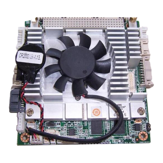
- Page 1 User Manual PCM-3363 ® PCI-104 SBC w/Intel Atom™ N455/D525, VGA, LVDS, Gigabit Ethernet, USB2.0, SATA, and on-board memory...
- Page 2 No part of this manual may be reproduced, copied, translated or transmitted in any form or by any means without the prior written permission of Advantech Co., Ltd. Information provided in this manual is intended to be accurate and reliable. How- ever, Advantech Co., Ltd.
- Page 3 Packing List Before you begin installing your card, please make sure that the following materials have been shipped: 1 x PCM-3363 SBC 1 x SATA data cable 7p 32 cm (w/locked) (p/n: 1700008941) 1 x SATA power cable (p/n: 1703150102) ...
- Page 4 Additional Information and Assistance Visit the Advantech web site at www.advantech.com where you can find the lat- est information about the product. Contact your distributor, sales representative, or Advantech's customer service center for technical support if you need additional assistance. Please have the following information ready before you call: ...
-
Page 5: Table Of Contents
2.14 GPIO Connector..................15 2.15 Power Input Connectors................15 2.16 SMBus connector..................15 2.17 -12 V power connector ................16 2.18 High Definition Audio Interface..............16 2.19 Watchdog Timer Configuration ............... 16 Chapter AMI BIOS Setup .........17 PCM-3363 User Manual... - Page 6 Save Changes and Exit .............. 35 3.8.2 Discard Changes and Exit ............35 3.8.3 Load Optimal Defaults ..............36 3.8.4 Load Fail-Safe Defaults .............. 36 Chapter Software Introduction & Installation S/W Introduction ..................38 Driver Installation ..................38 PCM-3363 User Manual...
- Page 7 DMA channel assignments ..............68 Table B.3: DMA channel assignments........68 Interrupt assignments................69 Table B.4: Interrupt assignments ..........69 Appendix C Watchdog Timer and GPIO Sample Code............71 Watchdog Timer sample code ..............72 GPIO Code....................73 PCM-3363 User Manual...
- Page 8 PCM-3363 User Manual viii...
-
Page 9: Chapter 1 General Information
Chapter General Information This chapter gives background information on the PCM-3363. Sections include: Introduction Features Specifications Board layout and dimensions... -
Page 10: Introduction
PCM-3363 uses an Intel® Atom™ N455/D525 processor, supporting on-board 1 GB DDRIII 800MHz SDRAM. PCM-3363 has an integrated graphics controller contains a refresh of the 3rd genera- tion graphics core with 224 MB shared memory. This feature makes PCM-3363 is... -
Page 11: Os Support
8-bit Programmable General Purpose Input/ Output Watchdog timer: Output System Reset, Programmable counter from 1 ~ 255 minutes/ seconds High Definition Audio: PCM-3363 can provide audio function with the optional audio extension module: PCA-AUDIO-HDA1E 1.2.1.7 BIOS AMI 16Mbit SPI Flash ROM 1.2.2... -
Page 12: Electrical Specifications
Environmental Operating temperature: 0 ~ 60° C (32 ~ 140° F) Operating Humidity: 40° C @ 85% RH Non-Condensing Storage Temperature: Storage temperature: -20~70° C Storage Humidity: Relative humidity: 95% @ 60° C PCM-3363 User Manual... -
Page 13: Block Diagram
I nt e rfa c e 8 -bit GPI O PCA9 5 5 5 BI OS 2 RS-2 3 2 Supe r I O K B/M S SCH 3 1 1 4 1 RS-4 2 2 /4 8 5 4 pins PCM-3363 User Manual... -
Page 14: Board Layout: Dimensions
Board layout: dimensions Figure 1.1 Board layout: Dimensions (Component Side) PCM-3363 User Manual... - Page 15 Figure 1.2 Board layout: Dimensions (Solder Side) PCM-3363 User Manual...
- Page 16 PCM-3363 User Manual...
-
Page 17: Chapter 2 Hardware Installation
Chapter Hardware Installation... -
Page 18: Jumpers
Jumpers The PCM-3363 has a number of jumpers that allow you to configure your system to suit your application. The table below lists the functions of the various jumpers. Table 2.1: Jumpers AT/ATX Power Setting RS485/422 Setting PCI VIO Setting... -
Page 19: Locating Connectors & Block Diagram
Locating Connectors & block diagram Figure 2.1 Connectors (component side) Figure 2.2 Connectors (solder side) PCM-3363 User Manual... -
Page 20: Setting Jumpers
2.4.1 AT/ATX Power Setting (J1) The PCM-3363 single board computer contains a jumper that can switch the AT/ATX Power Setting. Normally this jumper should be set with closed. It will send the power button signal to power on the system automatically. It also can keep open to power on the system by power button switch. -
Page 21: Com3 Rs422/Rs485 Select (J2)
Table 2.5: PCI I/O Voltage Select (J3) Setting Function 3.3 V 2.4.4 LVDS Panel Power Select (J4) Table 2.6: LVDS Panel Power Select (J4) Setting Function 3.3 V (default) PCM-3363 User Manual... -
Page 22: Compactflash
The CompactFlash card can be enabled/disabled via the BIOS settings. VGA/LCD interface connections The PCM-3363’s VGA interface can drive conventional CRT displays and is capable of driving a wide range of LVDS flat panel displays. The board has two connectors to support these displays: one for standard CRT VGA monitors, one for LVDS type LCD panels. -
Page 23: Buzzer Connector
PCM-3363 also equip one SATA power connector. It only can supply 5 V and less than 500 mA current to the Hard Drive. -
Page 24: 12 V Power Connector
2.17 -12 V power connector The PCM-3363 is equipped with a Negative Power Input connector providing -12 V power if applications happen to need it. 2.18 High Definition Audio Interface The PCM-3363 provides high definition audio interface. It can support high definition audio stereo by customized audio module that has codec onboard or by Advantech's PCA-AUDIO-HDA1E module through specific cable. -
Page 25: Chapter 3 Ami Bios Setup
Chapter AMI BIOS Setup... -
Page 26: Entering Setup
AMIBIOS has been integrated into kajillions of motherboards for well over a decade. With the AMIBIOS Setup program, you can modify BIOS settings and control the var- ious system features. This chapter describes the basic navigation of the PCM-3363 BIOS setup screens. -
Page 27: Main Setup
Date using the <Arrow> keys. Enter new values through the keyboard. Press the <Tab> key or the <Arrow> keys to move between fields. The date must be entered in MM/DD/YY format. The time must be entered in HH:MM:SS format. PCM-3363 User Manual... -
Page 28: Advanced Bios Features Setup
Advanced BIOS Features Setup Select the Advanced tab from the PCM-3363 setup screen to enter the Advanced BIOS Setup screen. You can select any of the items in the left frame of the screen, such as CPU Configuration, to go to the sub menu for that item. You can display an Advanced BIOS Setup option by highlighting it using the <Arrow>... -
Page 29: Ide Configuration
Hard Disk Write Protect Disable/Enable device write protection. This will be effective only if device is accessed through BIOS. IDE Detect Time Out (Sec) This item allows you to select the time out value for detecting ATA/ATAPI device(s). PCM-3363 User Manual... -
Page 30: Super I/O Configuration
Auto Flow Control For SP3 This item allows you to enable or disable auto flow control function. 3.3.4 Hardware Health Configuration Figure 3.7 Hardware health configuration H/W Health Function This item allows you to control H/W monitor display. PCM-3363 User Manual... -
Page 31: Acpi Settings
Figure 3.8 ACPI Settings 3.3.5.1 General ACPI Configuration Figure 3.9 General ACPI Configuration Suspend mode Select the ACPI state used for system suspend. Report Video on S3 Resume This item allows you to invoke VA BIOS POST on S3/STR resume. PCM-3363 User Manual... - Page 32 Include OEMB table pointer to R(x)SDT pointer lists. Headless mode Enable / Disable Headless operation mode through ACPI. 3.3.5.3 Chipset ACPI Configuration Figure 3.11 Chipset ACPI Configuration Energy Lake Feature Allows you to configure Intel's Energy Lake power management technology. PCM-3363 User Manual...
-
Page 33: Ahci Configuration
3.3.6 AHCI Configuration Figure 3.12 AHCI Configuration AHCI Ports0/Port1 While entering setup, BIOS auto detects the presence of IDE devices. This displays the status of auto detection of IDE device. 3.3.7 APM Configuration Figure 3.13 APM Configuration PCM-3363 User Manual... -
Page 34: Event Log Configuration
Figure 3.14 Event Log Configuration View Event Log View all unread events on the event Log. Mark all events as read Mark all unread events as read. Clear Event Log Discard all events in the event Log. PCM-3363 User Manual... -
Page 35: Mps Configuration
3.3.9 MPS Configuration Figure 3.15 MPS Configuration MPS Revision This item allows you to select MPS reversion. 3.3.10 Smbios Configuration Figure 3.16 Smbios Configuration Smbios Smi Support SMBIOS SMI wrapper support for PnP function 50h-54h. PCM-3363 User Manual... -
Page 36: Usb Configuration
A dummy FDD device is created that will be associated with the hotplugged FDD later. Auto option creates this dummy device only if there is no USB FDD present. 3.3.11.1 USB Mass Storage Device Configuration Figure 3.18 USB Mass storage Device Configuration PCM-3363 User Manual... -
Page 37: Advanced Pci/Pnp Settings
FDD (Ex. ZIP drive). Advanced PCI/PnP Settings Select the PCI/PnP tab from the PCM-3363 setup screen to enter the Plug and Play BIOS Setup screen. You can display a Plug and Play BIOS Setup option by highlight- ing it using the <Arrow> keys. All Plug and Play BIOS Setup options are described in this section. -
Page 38: Boot Settings
When set to Reserved will specify DMA will be Reserved for use by legacy ISA devices. Reserved Memory Size This item allows you to set memory block reserve size for legacy ISA devices. Boot Settings Figure 3.20 Boot Setup Utility PCM-3363 User Manual... -
Page 39: Boot Settings Configuration
Wait for the F1 key to be pressed if an error occurs. Hit ‘DEL’ Message Display Displays “Press DEL to run Setup” in POST. Interrupt 19 Capture This item allows option ROMs to trap interrupt 19. Bootsafe function This item allows you to enable or disable bootsafe function. PCM-3363 User Manual... -
Page 40: Security Setup
Security Setup Figure 3.22 Password Configuration Select Security Setup from the PCM-3363 Setup main BIOS setup menu. All Security Setup options, such as password protection and virus protection are described in this section. To access the sub menu for the following items, select the item and press <Enter>:... -
Page 41: North Bridge Chipset Configuration
Select the amount of system memory used by the Internal graphics device. Figure 3.25 Video function configuration DVMT Mode Select Displays the active system memory mode. DVMT/FIXED Memory Specify the amount of DVMT / FIXED system memory to allocate for video memory. PCM-3363 User Manual... -
Page 42: South Bridge Chipset Configuration
Enables or disables the HDA controller. SMBUS Controller Enables or disables the SMBUS controller. SLP_S4# Min. Assertion Width This item sets the minimum assertion width of the SLP-S4# signal to guarantee the DRAM has been safely power-cycled. PCM-3363 User Manual... -
Page 43: Exit Option
Select Exit Discarding Changes from the Exit menu and press <Enter>. The fol- lowing message appears: Discard Changes and Exit Setup Now? [Ok] [Cancel] Select Ok to discard changes and exit. Discard Changes Select Discard Changes from the Exit menu and press <Enter>. PCM-3363 User Manual... -
Page 44: Load Optimal Defaults
3.8.3 Load Optimal Defaults The PCM-3363 automatically configures all setup items to optimal settings when you select this option. Optimal Defaults are designed for maximum system performance, but may not work best for all computer applications. In particular, do not use the Opti- mal Defaults if your computer is experiencing system configuration problems. -
Page 45: Chapter 4 Software Introduction & Installation
Chapter Software Introduction & Installation... -
Page 46: S/W Introduction
S/W Introduction The mission of Advantech Embedded Software Services is to "Enhance quality of life with Advantech platforms and Microsoft Windows® embedded technology." We enable Windows® Embedded software products on Advantech platforms to more effectively support the embedded computing community. Customers are freed from the hassle of dealing with multiple vendors (hardware suppliers, system integrators, embedded OS distributors) for projects. -
Page 47: Software Apis
SUSI provides a consistent programming interface for different Advantech boards. That means user programs using SUSI are portable among different Advantech boards as long as the boards and SUSI provide the required functionalities. Overall product development times can be greatly reduced using SUSI. -
Page 48: Susi Utilities
However, due to the inaccuracy among many commercially available hardware mon- itoring chips, Advantech has developed a unique scheme for hardware monitoring - achieved by using a dedicated micro-processor with algorithms specifically designed for providing accurate, real-time and reliable data;... -
Page 49: Susi Installation
Windows CE In windows CE, there are three ways to install the SUSI Library, you can install it manually or use Advantech CE-Builder to install the library or just copy the programs and the library onto a compact flash card. -
Page 50: Susi Sample Programs
You can click function tabs to select test functions respectively. Some function tabs will not show on the test application if your platform does not support such functions. For a complete support list, please refer to Appendix A. We describe the steps to test all functions of this application. PCM-3363 User Manual... - Page 51 Click the radio button- Multiple-Pins. – Key in the pin number from ‘0x01’ to ‘0x0F’ to read the value of the input pin. The pin numbers are ordered bitwise, i.e. bit 0 stands for GPIO 0, bit 1 stands PCM-3363 User Manual...
- Page 52 Key in the register offset in Register Offset field. – Key in the desirous of data in Result field to write to the device. – Click the WRITE A BYTE button and then the data will be written to the device through I PCM-3363 User Manual...
- Page 53 – Key in the desired data, such as 0x1234, in the Result field to write to the device. – Click the WRITE SMBus DATA button and the data will be written to the device through the SMBus. PCM-3363 User Manual...
- Page 54 Move the slider in increments, using either the mouse or the direction keys, or click the UP button to increase the brightness. – Move the slider in decrements, using either the mouse or the direction keys, or click the DOWN button to decrease the brightness. PCM-3363 User Manual...
- Page 55 Before the timer counts down to zero, you can reset the timer by clicking the REFRESH button. After you click this button, the Timeout Countdown field will display the value of the SET TIMEOUT field. If you want to stop the watchdog timer, just click the STOP button. PCM-3363 User Manual...
- Page 56 If certain data values are not supported by the platform, the correspondent data field will be grayed-out with a value of 0. For More detail PCM-3363 software API user manual, please contact your dealer or Advantech AE. We also include these manuals in this DVD.
-
Page 57: Appendix A Pin Assignments
Appendix Pin Assignments This appendix contains informa- tion of a detailed or specialized nature. Sections include: Jumper and Connector Tables... -
Page 58: Jumper And Connector Tables
PIN HEADER 3*1P 180D(M) 2.0mm DIP SQUARE W/O Pb Description Setting Function (1-2) RS485 (2-3) RS422 PCI VIO Setting Part Number 1653003101 Footprint HD_3x1P_79_D Description PIN HEADER 3*1P 180D(M) 2.0mm DIP SQUARE W/O Pb Setting Function (1-2) +5 V (2-3) +3.3 V PCM-3363 User Manual... - Page 59 PIN HEADER 3*1P 180D(M) 2.0mm DIP SQUARE W/O Pb Description Setting Function (1-2) +5 V (2-3) +3.3 V Power Input 1655308120 Part Number WHL8H-2M Footprint Wafer Box 2.0mm 8P 90D Male W/Lock Description Pin Name +5 V +5 V +5 V +12 V PCM-3363 User Manual...
- Page 60 Footprint IC SKT 8P SMD WO/Pb C ACA-SPI-004-K01 Description Pin Name HOLD# +3.3 Part Number 1655912120 Footprint SP-12SMH Description Wafer Box 1.25mm 12P 90D(M) SMD 85204-12001 Pin Name GREEN BLUE DDAT DCLK HSYNC VSYNC Matching Cable: 1700000898 PCM-3363 User Manual...
- Page 61 Description Pin Name Power Button Pin1 Power Button Pin2 Reset Button Reset Button Power LED+ Power LED- HDD LED+ HDD LED- 1653002919 Part Number CF_50P_CFCMD-35T15W100 Footprint CF Type2 Conn.50P 90D(M) SMD WO/Pb CFCMD-35T15W1 Description Pin Name CS0# PCM-3363 User Manual...
- Page 62 CD2# CD1# CS1# VS1# IORD# IOWR# IREQ CSEL# VS2# RESET IORDY INPACK# REG# DASP# PDIAG# PCM-3363 User Manual...
- Page 63 SATA Part Number 1654004118 Footprint SATA_7P_50_WATA-07DPLH4U Serial ATA Con 7P 90D(M) SMD 1.27mm Description Pin Name SATA Power 1655302020 Part Number WF_2P_79_BOX_R1_D Footprint WAFER BOX 2P 180D(M) 2.0mm W/Lock Description Pin Name PCM-3363 User Manual...
- Page 64 Wafer box conn. DIP 2*5P 180D(M) 2.0mm NO.10P Description Pin Name A_D- B_D- A_D+ B_D+ Internal USB 1655002182 Part Number WF_5x2P_79_BOX_N10_D Footprint Wafer box conn. DIP 2*5P 180D(M) 2.0mm NO.10P Description Pin Name A_D- B_D- A_D+ B_D+ PCM-3363 User Manual...
- Page 65 CN10 COM1/COM2 1655003790 Part Number WF_10x2P_79_BOX_D Footprint WAFER BOX 2*10P 2mm 180D(M) DIP 24W2140-20S10-01 Description Pin Name DCD1# DSR1# RXD1 RTS1# TXD1 CTS1# DTR1# RI1# DCD2# DSR2# RXD2 RTS2# TXD2 CTS2# DTR2# RI2# PCM-3363 User Manual...
- Page 66 WAFER BOX 2.0mm 4P 90D(M) DIP W/LOCK Description Pin Name 422RX- 422RX+ 422/485TX+ 422/485TX- CN13 PS/2 Part Number 1655306020 WHL6V-2M Footprint WAFER BOX 2.0mm 6P 180D(M) W/LOCK Description Pin Name KBCLK KBDAT MSCLK MSDAT Matching Cable: 1703060053 1703060191 1700060202 PCM-3363 User Manual...
- Page 67 PIN HEADER 8*1P 180D(M) SQUARE 2.0mm Description Pin Name BITCLK SYNC RST# SDIN SDOUT +V12 CN15 SMBus (I 1655904020 Part Number FPC4V-125M Footprint Wafer SMT 1.25mmS/T type 4P 180D(M) 85205-04001 Description Pin Name SMB_DAT SMB_CLK +5 V PCM-3363 User Manual...
- Page 68 Part Number WHL3V-2M Footprint WAFER BOX 2.0mm 3P 180D w/LOCK Description Pin Name Speed CN17 GPIO 1653010102 Part Number JH10X1V-2M Footprint PIN HEADER 10*1P 180D P=2.0mm Description Pin Name GPIO0 GPIO1 GPIO2 GPIO3 GPIO4 GPIO5 GPIO6 GPIO7 PCM-3363 User Manual...
- Page 69 Footprint Wafer 2.00mm 2*5P 180D(M) DIP W/LOCK WO/Pb Description Pin Name BI_DD+(GHz) BI_DD-(GHz) BI_DC+(GHz) BI_DC-(GHz) RX+(10/100),BI_DB+(GHz) RX-(10/100),BI_DB-(GHz) TX+(10/100),BI_DA+(GHz) TX-(10/100),BI_DA-(GHz) CN21 Buzzer 1655902032 Part Number WHL2V-125 Footprint Description WAFER 2P 180D(M) 1.25mm DIP 53047-0210 Pin Name Buzzer+ Buzzer- PCM-3363 User Manual...
- Page 70 +3.3V PA18 IDSEL0 PA19 AD24 PA20 PA21 AD29 PA22 PA23 REQ0# PA24 PA25 GNT1# PA26 PA27 CLK2 PA28 PA29 +12V PA30 -12V AD02 AD07 AD09 VI/O (+5V or +3.3V) AD13 C/BE1# PB10 PERR# PB11 +3.3V PB12 TRDY# PCM-3363 User Manual...
- Page 71 PC11 LOCK# PC12 PC13 IRDY# PC14 +3.3V PC15 AD17 PC16 PC17 AD22 PC18 IDSEL1 PC19 VI/O (+5V or +3.3V) PC20 AD25 PC21 AD28 PC22 PC23 REQ1# PC24 PC25 GNT2# PC26 PC27 CLK3 PC28 PC29 INTB# PC30 GNT3# PCM-3363 User Manual...
- Page 72 PD11 PD12 DEVSEL# PD13 +3.3V PD14 C/BE2# PD15 PD16 AD19 PD17 +3.3V PD18 IDSEL2 PD19 IDSEL3 PD20 PD21 AD27 PD22 AD31 PD23 VI/O (+5V or +3.3V) PD24 GNT0# PD25 PD26 CLK1 PD27 PD28 RST# PD29 INTC# PD30 PCM-3363 User Manual...
- Page 73 PIN HEADER 2*1P 180D(M)SQUARE 2.0mm DIP W/O Pb Description Pin Name -12V CN24 Inverter Power Output 1655000453 Part Number Footprint WHL5V-2M-24W1140 Description WAFER BOX 2.0mm 5P 180D(M) DIP WO/Pb JIH VEI Pin Name +12 V ENABKL +5 V PCM-3363 User Manual...
- Page 74 24 bits LVDS Panel 1653910261 Part Number SPH10X2 Footprint *CONN. SMD 10*2P 180D(M)DF13-20DP-1.25V(91) HRS Description Pin Name LVDS0_D0+ LVDS0_D0- LVDS0_D1+ LVDS0_D1- LVDS0_D2+ LVDS0_D2- LVDS0_CLK+ LVDS0_D3+ LVDS0_CLK- LVDS0_D3- +5 V or +3.3 V +5 V or +3.3 V PCM-3363 User Manual...
-
Page 75: Appendix B System Assignments
Appendix System Assignments This appendix contains informa- tion of a detailed nature. Sections include: System I/O ports 1st MB memory map DMA channel assignments Interrupt assignments... -
Page 76: System I/O Ports
Function Available Available (audio) Floppy disk (8-bit transfer) Available (parallel port) Cascade for DMA controller 1 Available Available Available * Audio DMA select 1, 3, or 5 ** Parallel port DMA select 1 (LPT2) or 3 (LPT1) PCM-3363 User Manual... -
Page 77: Interrupt Assignments
COM1 IRQ 5 Reserved IRQ 6 Reserved IRQ 7 Reserved IRQ 8 IRQ 9 Reserved IRQ 10 Reserved IRQ 11 COM3 IRQ 12 PS/2 mouse IRQ 13 Math coprocessor IRQ 14 Primary IDE IRQ 15 Secondary IDE PCM-3363 User Manual... - Page 78 PCM-3363 User Manual...
-
Page 79: Watchdog Timer And Gpio Sample Code
Appendix Watchdog Timer and GPIO Sample Code... -
Page 80: Watchdog Timer Sample Code
;Minutes=0 (default) Seconds=1 ;==================================================== mov dx,SCH3114_IO + 65h ; mov al,080h out dx,al ;==================================================== ;66H ;WDT timer time-out value ;bit[7:0]=0~255 ;==================================================== mov dx,SCH3114_IO + 66h mov al,01h out dx,al ;==================================================== ;bit[0] status bit R/W ;WD timeout occurred =1 PCM-3363 User Manual... -
Page 81: Gpio Code
; n means which group of GPIO you want to set bl= the n group of gpio config bit 0 = gpio 0 , 0 => output pin; 1 => input pin bit 1 = gpio 1 , 0 => output pin; 1 => input pin ..PCM-3363 User Manual... - Page 82 1 = gpio 1 , 0 => Low; 1 => High ..bit 7 = gpio 7 , 0 => Low; 1 => High ; output: ax=5E78 ;function success, other value means function fail ;=============================================================== ax,5e87h bh,00h ax,5e78h next_test dx, Error_Str1 ah,09h Finish_Test next_test: PCM-3363 User Manual...
- Page 83 ;4. Set GPIO 0,2,4,6 Output differential ;restore NO. of GPIO chip push ;save NO. of GPIO chip ax,5e87h bx,0411h ;5. Check GPI 1,3,5,7 value ;restore NO. of GPIO chip push ;save NO. of GPIO chip ax,5e87h bx,03FFh ;restore NO. of GPIO chip PCM-3363 User Manual...
- Page 84 ;restore NO. of GPIO chip push ;save NO. of GPIO chip ax,5e87h bx,0300h ;restore NO. of GPIO chip push ;save NO. of GPIO chip al,Fail_lenght dx, Fail_Str dx,ax bl,0ffh test_result ;4. Set GPIO 1,3,5,7 Output differential ;restore NO. of GPIO chip PCM-3363 User Manual...
- Page 85 ;restore NO. of GPIO chip push ;save NO. of GPIO chip al,Success_lenght dx, Success1_Str dx,ax ;Do Second PCA9554 test ;1.Set GPIO 0,2,4,6 as output, GPI 1,3,5,7 as input test_result: ah,09h next_test Finish_Test: popa .exit PCM-3363 User Manual...
- Page 86 No part of this publication may be reproduced in any form or by any means, electronic, photocopying, recording or otherwise, without prior written permis- sion of the publisher. All brand and product names are trademarks or registered trademarks of their respective companies. © Advantech Co., Ltd. 2011...
Need help?
Do you have a question about the PCM-3363 and is the answer not in the manual?
Questions and answers