Table of Contents
Advertisement
Quick Links
Advertisement
Table of Contents

Related Manuals for Octek RHINO 5


Summary of Contents for Octek RHINO 5
- Page 1 USER'S MANUAL RHINO 5 Pentium PCI Local Bus Motherboard...
- Page 2 RHINO 5 Pentium PCI Local Bus Motherboard User’s Manual Version 1.0 August 1995...
- Page 3 Trademarks Intel i486, Pentium and Intel are registered trademarks of Intel Corporation. Octek is a registered trademark of Ocean Office Automation Ltd. OPTi is a registered trademark of OPTi Inc. XT, AT, PS/2, OS/2, & IBM are registered trademarks of International Business Machines Corporation.
- Page 4 Preface About the Rhino 5 Thank you for purchasing the Rhino 5, Ocean’s new top-of-the- line Pentium motherboard. The Rhino 5 utilizes advanced PCI architecture that takes personal computing to a new level of performance. About the Manual The content of this manual is for reference only and is intended to provide basic information for the general user.
-
Page 5: Table Of Contents
Table of Contents Preface Chapter 1: System Overview General Specification Overview ........2 Central Processing Unit ...........5 External Cache Subsystem ..........5 DRAM Subsystem ............5 PCI Bus ................6 Super I/O Subsystem ............6 Input/Output Subsystem ...........7 BIOS Subsystem ..............7 Chapter 2: Installation and Upgrade Setup .................8 Installation Precautions ............8 Operation and Maintenance ..........8... - Page 6 Appendix-A: Advanced Technical Information Memory Address Map ...........16 I/O Address Map ............17 I/O Extension Pinout .............18 A.3i 8-Bit ISA Pinout ...........18 A.3ii 16-Bit ISA Extension Pinout ........19 PCI Bus Pinout ..............20 Direct Memory Access Channels ........21 DMA Controller Registers ..........21 Page Register Address ...........22 System Interrupts ............22 Appendix-B: Connectors Pinout...
- Page 7 System Component Map ..........30 Layout of RHINO 5 Main Board .........31 Jumper Settings .............32 C.3.1 CPU related settings ........32 C.3.2 External cache (L2 cache) setting ....35 C.3.3 DRAM ............36 C.3.4 Peripheral setup ..........37 C.3.5 Miscellaneous ...............38...
-
Page 8: Chapter 1: System Overview
Chapter 1 System Overview CHAPTER 1 SYSTEM OVERVIEW OCTEK RHINO 5 is a powerful PC machine offering unparalleled performance. The advanced external cache system implemented meets the demand of the most memory-intensive applications today. With the Pentium processor and a high bandwidth 32-bit PCI expansion bus, the I/O bottleneck that plagues most PC systems is now removed. -
Page 9: General Specification Overview
3 x 16-bit ISA slots shared bus slots 1 x 32 bit PCI bus slot (master) OR 1 x 16-bit ISA slot I/O bus speed Up to 33MHz (PCI bus) Integrated IDE, Super I/O Subsystem RHINO 5 User’s Manual... - Page 10 Password protection, Shadowing options Plug & Play / BIOS Update Plug & Play BIOS Support Plug & Play for easy installation Flash EEPROM Use Flash EEPROM (1M bits) to allow easy BIOS update RHINO 5 User’s Manual...
- Page 11 On board 3.3V supply to eliminate the need for special power supply for 3.3V component e.g. CPU, SRAM. Maximum rating : 30 W. Switches EPMI, Reset, Keylock switches Size 8.5" (W) x 13" (L) RHINO 5 User’s Manual...
-
Page 12: Central Processing Unit
SRAM can be used in RHINO 5. DRAM Subsystem The main memory in RHINO 5 is organized as a 64-bit memory pool. Both fast-page mode and EDO DRAMs are supported. EDO DRAM stands for Extended Data Out DRAM and is designed to improve the DRAM read performance. -
Page 13: Pci Bus
The PCI local bus implemented in RHINO 5 is fully compliant to v2.0 specification. Up to four PCI bus masters are supported. Advanced PCI bus buffer management logic speeds to the transfer rate. -
Page 14: Input/Output Subsystem
IRQ 12. Nevertheless, user can disable the PS/2 mouse function by means of jumpers. Input/Output Subsystem To allow greater system feasibility, RHINO 5 has four ISA bus expansion connectors and four PCI expansion connectors. One of the expansion slots is shared by connectors that will accommodate either an ISA or a PCI expansion, but not both at the same time. -
Page 15: Chapter 2: Installation And Upgrade
Chapter 2 Installation and Upgrade CHAPTER 2 INSTALLATION AND UPGRADE Setup Before installing the Rhino 5 motherboard in your system, you must attach the peripheral connectors. Follow the instructions outlined in this chapter for proper installation. Installation Precautions • Turn off the power whenever installing or removing any connectors, memory module or add-on cards. -
Page 16: Cpu Installation
CPU onto the SPGA socket located on RHINO 5 (refer to layout for exact location). To properly align the CPU with the socket, align pin 1 of the CPU ( with a notch at the corner) with pin 1 of the CPU socket as demonstrated below. -
Page 17: Cpu Upgrade/ Vrm Header
(about 3.3.V) has already provided by the mainboard. Inside RHINO 5 motherboard, you will find the VRM header (Header 7) which is stuffed with four jumper shunts. To install the VRM , remove the four jumper shunts and insert the VRM into the header. -
Page 18: Fast Page Mode / Edo Dram Installation
Chapter 2 Installation and Upgrade Fast Page mode / EDO DRAM Installation There are four memory banks located on the RHINO 5 motherboard, marked SM1, SM2, SM3 and SM4. The SM1, SM2, SM3 and SM4 are counted starting from right to left consecutively. - Page 19 The latches should be locked tightly and the holes in the module should be aligned with the tabs on the bank. → Near KB Connector Figure 3 Proper Memory Module Installation RHINO 5 User’s Manual...
- Page 20 Chapter 2 Installation and Upgrade Below is the memory configuration table for RHINO 5. Total -------- -------- 256Kx32 256Kx32 -------- -------- 512Kx32 512Kx32 -------- -------- 1Mx32 1Mx32 -------- -------- 2Mx32 2Mx32 16MB -------- -------- 4Mx32 4Mx32 32MB -------- -------- 8Mx32...
-
Page 21: Asynchronous Cache Ram Installation
Chapter 2 Installation and Upgrade Asynchronous Cache RAM Installation RHINO 5 provides the option for changing the size of the asynchronous cache RAM from cacheless up to 1M bytes cache RAM. To do this, besides the jumper settings mentioned in the Appendix C has to be set properly, care must be taken to stuff the cache RAM in the proper place and orientation. -
Page 22: Fan Voltage
Next, set the jumper JP21 back to 2-3 and turn on the power. The BIOS will find the CMOS status register is reset and will regard the setup information invalid, so it will prompt you to correct the information. RHINO 5 User’s Manual... -
Page 23: Appendix-A: Advanced Technical Information
System board memory 00A0000- 128 KB Video RAM display 00BFFFF buffer 00C0000- 128 KB Reserved for add-on cards 00DFFFF ROM BIOS 00E0000-00EFFFF 64 KB System ROM BIOS expansion 00F0000-00FFFFF 64 KB System ROM BIOS 0100000-7FFFFFF 127MB Extended memory RHINO 5 User’s Manual... -
Page 24: I/O Address Map
PC Network, High Address 378-37F Parallel Printer Port 1 (PIO-1) 380-38F SDLC, Bisynchronous 2 3A0-3AF Bisynchronous 1 3B0-3BF Monochrome Display and Primer Adapter 3C0-3CF EGA Adapter 3D0-3DF Color/Graphics Monitor Adapter 3F0-3F7 Diskette Controller 3F8-3FF Serial Port 1 (SIO-1) RHINO 5 User’s Manual... -
Page 25: I/O Extension Pinout
Power +12 VDC Ground -I/O CHRDY -SMEMW -SMEMR SA19 -IOW SA18 -IOR SA17 -DACK3 SA16 DRQ3 SA15 -DACK1 SA14 DRQ1 SA13 -Ref SA12 SA11 IRQ7 SA10 IRQ6 IRQ5 IRQ4 IRQ3 -DACK2 BALE Power +5 VDC Ground RHINO 5 User’s Manual... -
Page 26: A.3Ii 16-Bit Isa Extension Pinout
-I/OCS16 LA23 IRQ10 LA22 IRQ11 LA21 IRQ12 LA20 IRQ15 LA19 IRQ14 LA18 -DACK0 LA17 DRQ0 -MEMR -DACK5 -MEMW DRQ5 SD08 -DACK6 SD09 DRQ6 SD10 -DACK7 SD11 DRQ7 SD12 Power +5 VDC SD13 -MASTER SD14 Ground SD15 RHINO 5 User’s Manual... -
Page 27: Pci Bus Pinout
FRAME# IRDY# GROUND RESERVED TRDY# DEVSEL# GROUND GROUND STOP# LOCK# RESERVED PERR# SDONE RESERVED SBO# SERR# GROUND RESERVED C/BE[1]# AD[15] AD[14] RESERVED GROUND AD[13] AD[12] AD[11] AD[10] GROUND GROUND AD[09] AD[08] C/BE[0]# AD[07] RESERVED RESERVED AD[06] RHINO 5 User’s Manual... -
Page 28: Direct Memory Access Channels
PCI Bus Pinout (Cont.) Direct Memory Access Channels Channe Function 8-Bit 16-Bit Transfer Block Size Spare 8-bit SDLC 8-bit Floppy Disk 8-bit Spare 8-bit Cascade for DMA controller 1 Spare 16-bit Spare 16-bit Spare 16-bit DMA Controller Registers RHINO 5 User’s Manual... -
Page 29: Page Register Address
DMA Channel 0 0087 DMA Channel 1 0083 DMA Channel 2 0081 DMA Channel 3 0082 DMA Channel 5 008B DMA Channel 6 0089 DMA Channel 7 008A Refresh 008F System Interrupts Interrupt Parity or I/O Channel Check RHINO 5 User’s Manual... - Page 30 Software Redirected to INT 0AH (IRQ2) IRQ10 Reserved IRQ11 Reserved IRQ12 PS/2 Mouse IRQ13 Coprocessor IRQ14 Fixed Disk Controller IRQ15 Reserved IRQ3 Serial Port 2 IRQ4 Serial Port 1 IRQ5 Parallel Port 2 IRQ6 Diskette Controller IRQ7 Parallel Port 1 RHINO 5 User’s Manual...
-
Page 31: Appendix-B: Connectors Pinout
CONNECTORS PINOUT Reset Connector (P1) Signal Name Reset Ground Turbo LED Connector (P2) Signal Name Pull_Up_150 LED_Turbo- Keylock Connector (P3) Signal Name +5Vdc Mechanical Key Ground Keyboard Inhibit Ground Fan Connector (P4) Signal Name +5/+12dc Power Ground RHINO 5 User’s Manual... -
Page 32: Epmi/T.b. Switch (P5)
Ground Ground Ground Ground +12Vdc V/IO V/IO V/IO +3.3Vdc +3.3Vdc +3.3Vdc +3.3Vdc VCORE VCORE VCORE VCORE Ground VCORE VCORE VCORE N.C. UPVRM# Sense N.C. Ground Ground +5Vdc +5Vdc +5Vdc +5Vdc External Battery Connector (P9) Signal Name RHINO 5 User’s Manual... -
Page 33: Ide Led Connector (P10)
Data 15 Ground DRQx Ground I/O Write- Ground I/O Read- Ground IOCHRDY BALE DACKx Ground IRQ14/15* IOCS16- Signal Name Signal Name Address 1 N.C. Address 0 Address 2 Chip Select 0- Chip Select 1- Activity Ground RHINO 5 User’s Manual... -
Page 34: Floppy Connector (P13)
Write Protect- Ground Read Data- Ground Side 1 Select- Ground Disk Change B.12 Printer Port Connector (P14) Signal Name Signal Name STROBE- AUTO FEED- Data bit 0 ERROR- Data bit 1 INIT- Data bit 2 SLCT IN- RHINO 5 User’s Manual... -
Page 35: Serial Port Connector (P15,P16)
Data bit 4 Ground Data bit 5 Ground Data bit 6 Ground Data bit 7 Ground ACK- Ground BUSY Ground PE (Paper End) Ground SLCT N.C. B.13 Serial Port Connector (P15,P16) Signal Name Signal Name Ground N.C. RHINO 5 User’s Manual... -
Page 36: Power Connector (P17,P18)
PS/2 Mouse Connector (P19) Signal Name Signal Name +5V dc N.C. N.C. N.C. Data N.C. Ground Clock B.16 Keyboard Connector (KB1) Signal Name Keyboard clock Keyboard data Not used Ground Note: KB1 is a DIN5 socket. RHINO 5 User’s Manual... -
Page 37: System Component Map
EPMI/TB Switch Speaker Header 7 External Battery Connector IDE LED Connector Secondary IDE Connector Primary IDE Connector Floppy Drive Connector Printer Port Serial Port 1 Serial Port 2 Power Connector Power Connector PS/2 Mouse Connector Keyboard Connector RHINO 5 User’s Manual... -
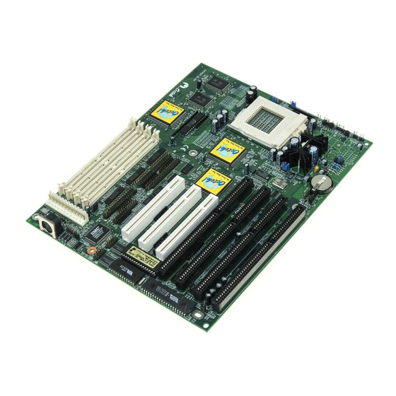
Page 38: Layout Of Rhino 5 Main Board
Appendix-C Hardware Settings Layout of RHINO 5 Main Board RHINO 5 User’s Manual... -
Page 39: Jumper Settings
CPUs P54C, P54CQS and P54CS. For P55C CPU, the processor will be used in connection with an Voltage Regulator Module (VRM). All the four shunt connectors installed in P8 should be removed. An VRM should be plugged in P8 instead. RHINO 5 User’s Manual... - Page 40 Appendix-C Hardware Settings TOP VIEW OF HEADER 7 (BESIDE THE CPU SOCKET) Figure 4 Top View of Header 7 CPU Clock RHINO 5 User’s Manual...
- Page 41 P54CS P54CS P55C P54CQS B-STEP C-STEP reserved reserved x2.5 x2.5 reserved reserved reserved reserved x1.5 x1.5 x1.5 reserved Multiplier selection based on CPU type JP39 Intel P54C-75 Intel P54C-90 Intel P54C-100 Intel P54C-120 Intel P54C-133 Cyrix RHINO 5 User’s Manual...
-
Page 42: C.3.2 External Cache (L2 Cache) Setting
C.3.2 External cache (L2 cache) setting Async Cache/ Sync Cache selection JP42 Asynchronous Cache Synchronous Cache Asynchronous L2 cache size JP10 256KB 512KB Voltage source for asynchronous L2 cache JP12 JP13 JP14 JP15 +5V supply +3.3V supply RHINO 5 User’s Manual... -
Page 43: C.3.3 Dram
Install a 32Kx8 5V tag SRAM at location U8. C.3.3 DRAM DRAM Type JP28 Fast page mode DRAM(60ns or 70ns) EDO DRAM(60ns or 70ns) EDO DRAM SIMMs are NOT allowed to be mixed with Fast- page mode DRAM SIMMs. RHINO 5 User’s Manual... -
Page 44: C.3.4 Peripheral Setup
2-3 * 2-3 * Disabled Printer port interrupt JP31 IRQ5 IRQ7 2-3 * DMA request for printer port ECP mode JP32 DRQ1 1-2 * DRQ3 DMA acknowledge for printer port ECP mode JP33 DACK1 1-2 * DACK3 RHINO 5 User’s Manual... -
Page 45: C.3.5 Miscellaneous
JP40 External Power Good 1-2 * On-board Power Good CMOS discharge JP21 Clear CMOS Preserve CMOS 2-3 * Battery select JP20 External Battery On-board Battery 2-3 * Reserved Jumpers JP22 JP27 2-3 PCI clock = CPUclock/2 RHINO 5 User’s Manual...
Need help?
Do you have a question about the RHINO 5 and is the answer not in the manual?
Questions and answers