Table of Contents
Advertisement
Quick Links
Advertisement
Table of Contents

Related Manuals for Octek Hippo COM


Summary of Contents for Octek Hippo COM
- Page 1 HIPPO COM...
- Page 2 The material in this manual is for information only and is subject to change without notice. REVISION: 1.1 IBM, IBM PC/XT/AT, PC-DOS, MS-DOS, OS/2, INTEL, AMI ARE THE TRADEMARKS OR REGISTERED TRADEMARKS OF THEIR RESPECTIVE OWNERS.
- Page 3 RADIO FREQUENCY INTERFERENCE STATEMENT This equipment generates and uses radio frequency energy and if not installed and used properly, that is, in strict accordance with the manufacturer's instructions, may cause interference with radio and television reception. If this equipment does cause interference to radio or TV reception, which can be determined by turning the equipment off and on, the user is encouraged to try to correct the interference by one or more of the following measures:...
- Page 4 Note 1.Electronic components are sensitive to dust and dirt. Do inspect and clean the computer system regularly. 2.Turn off the power whenever you install or remove any connector, memory module and add-on card. Before turning on the power, make sure that all the connectors, memory modules and add-on cards are secured.
- Page 5 There are also technical information for hardware and software engineers. In this manual, there are 4 chapters. Chapter 1 contains a brief introduction and specification of HIPPO COM motherboard. In the Chapter 2, the functions of HIPPO COM are explained.
-
Page 6: Table Of Contents
Table of Content Chapter 1 INTRODUCTION Chapter 2 GENERAL FEATURES Specification Chapter 3 CONFIGURING THE SYSTEM Installing RAM Modules Configuration of Memory DRAM Configuration Control of System Speed System Board Jumper Setting System Board Connectors Chapter 4 TECHNICAL INFORMATION Memory Mapping I/O Address Map System Timers System Interrupts... - Page 7 Appendix A OPERATION AND MAINTENANCE Static Electricity Keeping The System Cool Cleaning The `Golden Finger' Cleaning The Motherboard Appendix B SUMMERY OF JUMPER SETTING Appendix C SYSTEM BOARD LAYOUT...
- Page 9 It contains the most powerful microprocessor 80486 which combines CPU, numeric coprocessor and internal cache memory on a single chip. HIPPO COM fully takes advantage of the power of 80486 and provides high performance, reliability and compatibility to the user.
- Page 10 INTRODUCTION __________________________________________________________________________ THE PAGE IS INTENTIONALLY LEFT BLANK _________________________________________________________________________...
-
Page 11: Chapter 2 General Features
Chapter 2 General Features ___________________________________________________________ SPECIFICATION Processor : Intel 80486DX, 80486DX2, 80486SX or 80487SX CPU Speed : Turbo/normal speed I/O Slot : Compatible to standard AT bus Four 16-bit slots Memory : Shadow RAM for system and video BIOS Page mode and hidden refresh Flexible configuration SIMM sockets for 256KB, 1MB or 4MB modules _________________________________________________________________________... - Page 12 GENERAL FEATURES _________________________________________________________________________ Cache : 8KB four way set associative internal cache System Support Functions : 8-Channel DMA (Direct Memory Access) 16-level interrupt 3 programmable timers CMOS RAM for system configuration Real time clock with battery back-up Fast A20 gate and fast reset Other Features : External battery connector _________________________________________________________________________...
- Page 13 It is fully binary compatible with 80386 and 80387. All existing software for PC XT/AT can be used on HIPPO COM. However, due to the new internal architecture, the performance of 80486 is two to four times of 80386.
- Page 14 GENERAL FEATURES _________________________________________________________________________ _________________________________________________________________________...
- Page 15 GENERAL FEATURES _________________________________________________________________________ _________________________________________________________________________...
- Page 16 GENERAL FEATURES _________________________________________________________________________ The cache memory is a 8K bytes, 16 bytes line size, four-way set associative configuration. The hit rate of this configuration is much better than 32K bytes two-way set associative external cache because a four-way set associative architecture provides better performance in a multitasking and multi-processor environment.
- Page 17 GENERAL FEATURES _________________________________________________________________________ By eliminating the access to external bus, operations with the internal cache can be completed in a single cycle. 80386 at least needs two cycles for an operation. To further increase the rate of data transfer inside the CPU, the internal bus of the cache memory is increased to 128 bits, which is four times of the external bus.
- Page 18 GENERAL FEATURES _________________________________________________________________________ Internal memory management unit provides a flexible addressing scheme for the next generation operation system. Multitasking, concurrent operation and manipulating huge data base can be accomplished with excellent performance. Paging mechanism is employed to allow powerful operating system to implement virtual memory.
- Page 19 GENERAL FEATURES _________________________________________________________________________ MEMORY SYSTEM Two banks of DRAMs can be installed on board. So 8 SIMM modules may be installed on your system and the maximum memory size is up to 64MB. 256KB, 1MB, 4MB & 16MB DRAM SIMM modules are supported.
- Page 20 In the original PC/AT design, the memory refresh operation will suspend the CPU operation because it has to access the main memory. In a high speed system like HIPPO COM, the CPU indeed can process a large amount of operations in the memory refresh period.
- Page 21 An application without modification may cause problem. In HIPPO COM, there are some logic designs in the chipset to emulate the keyboard controller. An application can work in the usual way to send commands to keyboard controller, but these commands are in fact interpreted by the chipset.
- Page 22 GENERAL FEATURES _________________________________________________________________________ THIS PAGE IS INTENTIONALLY LEFT BLANK _________________________________________________________________________ 2-12...
-
Page 23: Configuring The System
Important Note : Turn off the power before installing or replacing any component. INSTALLING RAM MODULES HIPPO COM has eight 30-pin SIMM sockets on board for SIMM modules memory. Whenever you add memory to the motherboard, install four 30-pin SIMM modules at the same time. Also make sure that the chips on the modules face towards the slot for memory expansion board. -
Page 24: Configuration Of Memory
CONFIGURING THE SYSTEM _________________________________________________________________________ If the BIOS reports an memory error or parity error, drag out the modules and insert them again. If the locking latches are damaged, contact your dealer to replace the socket. CONFIGURATION OF MEMORY The configuration of the memory is very flexible. There are several combinations of DRAM types you may consider. -
Page 25: Dram Configuration
CONFIGURING THE SYSTEM _________________________________________________________________________ Because of the shadow RAM function, the 384KB memory between 640KB to 1MB can not accessed. So, the memory size found by the system BIOS is not equal to the actual memory size. For example, when there is 4MB on board, the BIOS will show 3712KB. DRAM CONFIGURATION Bank 0 Bank 1... -
Page 26: Control Of System Speed
CONFIGURING THE SYSTEM _________________________________________________________________________ CONTROL OF SYSTEM SPEED System speed can be controlled by keyboard and turbo switch. To change the speed by keyboard, use `-' and `+' of the numeric keypad. Press `Ctrl' `Alt' and `-' for slow speed and press `Ctrl' `Alt' and `+' for fast speed. -
Page 27: System Board Jumper Setting
CONFIGURING THE SYSTEM _________________________________________________________________________ SYSTEM BOARD JUMPER SETTING There are several options which allows user to select by hardware switches. CPU Type *486DX 486SX OPEN 487SX System Speed MX CLOCK CHIP Speed 25MHz *33MHz 40MHz 50MHz IMI CLOCK CHIP Speed 25MHz *33MHz 40MHz... - Page 28 CONFIGURING THE SYSTEM _________________________________________________________________________ to refer to. Make sure the 'System Speed' setting matched with the CPU speed rating. _________________________________________________________________________...
- Page 29 CONFIGURING THE SYSTEM _________________________________________________________________________ Display Selection DISPLAY TYPE Monochrome * CGA/EVA/VGA CMOS Jumper JP19 CMOS OPTION NORMAL OPERATION * RESET CMOS SETUP _________________________________________________________________________...
- Page 30 CONFIGURING THE SYSTEM _________________________________________________________________________ I/O SYSTEM ON-BOARD IDE ENABLE * DISABLE ON-BOARD FLOPPY ENABLE * DISABLE JP10 ON-BOARD GAME PORT ENABLE * DISABLE JP11 ON-BOARD PRINTER PORT ENABLE * DISABLE JP12 PRINTER PORT SELECT LPT2 (378) * LPT3 (278) _________________________________________________________________________...
- Page 31 CONFIGURING THE SYSTEM _________________________________________________________________________ JP14 ON-BOARD SERIAL PORT #1 ENABLE * DISABLE JP15 SERIAL PORT #1 SELECT COM1 (3F8) * COM3 (3E8) JP17 ON-BOARD SERIAL PORT #2 ENABLE * DISABLE JP18 SERIAL PORT #2 SELECT COM2 (2F8) * COM4 (2E8) _________________________________________________________________________...
-
Page 32: System Board Connectors
CONFIGURING THE SYSTEM _________________________________________________________________________ SYSTEM BOARD CONNECTORS Under typical conditions, these connectors should be connected to the indicators and switches of the system unit. The functions of connectors on the motherboard are listed below. Description Hardware reset connector Turbo switch connector Harddisk activity LED connector Turbo LED cwnector Power LED &... - Page 33 CONFIGURING THE SYSTEM _________________________________________________________________________ Pin assignment of the connector are illustrated as follows: P1 - Hardware Reset Connector Assignment Selection Pin Ground P2 - Turbo Switch Connector Assignment Selection Pin Ground P4 - Turbo LED Connector Assignment +5Vdc LED signal _________________________________________________________________________ 3-11...
- Page 34 CONFIGURING THE SYSTEM _________________________________________________________________________ P5 - Power LED & Ext-Lock Connector Assignment +5 Vdc Ground Keyboard inhibit Ground P6 - Speaker Connector Assignment Data out +5 Vdc Ground +5 Vdc _________________________________________________________________________ 3-12...
- Page 35 CONFIGURING THE SYSTEM _________________________________________________________________________ P13-P14 - Power Supply Connector Assignment POWERGOOD +5 Vdc +12 Vdc -12 Vdc Ground Ground Assignment Ground Ground -5 Vdc +5 Vdc +5 Vdc +5 Vdc _________________________________________________________________________ 3-13...
- Page 36 CONFIGURING THE SYSTEM _________________________________________________________________________ P15 - External Battery Connector Assignment + Vdc not used Ground Ground P16 - Cooling Fan connector Assignment + 5Vdc Ground KB1 - Keyboard Connector Assignment Keyboard clock Keyboard data Spare Ground +5 Vdc _________________________________________________________________________ 3-14...
- Page 37 CONFIGURING THE SYSTEM _________________________________________________________________________ THIS PAGE IS INTENTIONALLY LEFT BLANK _________________________________________________________________________ 3-15...
-
Page 39: Technical Information
Chapter 4 Technical Information ___________________________________________________________ This section provides technical information about HIPPO COM and is intended for advanced users interested in the basic design and operation of HIPPO COM. MEMORY MAPPING Address Range Function 000000-7FF 000K-512K System Board Memory (512K) - Page 40 800000-FFF 8192K-16318K System Memory _________________________________________________________________________...
-
Page 41: I/O Address Map
TECHNICAL INFORMATION _________________________________________________________________________ I/O ADDRESS MAP I/O Address Map on System Board I/O address hex 000 to 0FF are reserved for the system board I/O. ADDRESS DEVICE (HEX) 000-01F DMA Controller 1, 8237 020-03F Interrupt Controller 1, 8259, Master 040-05F Timer, 8254 060-06F Keyboard Controller... - Page 42 TECHNICAL INFORMATION _________________________________________________________________________ I/O address hex 100 to 3FF are available on the I/O channel. ADDRESS DEVICE (HEX) 1F0-1F8 Fixed Disk 200-207 Game I/O 278-27F Parallel Printer Port 2 2F8-2FF Serial Port 2 300-31F Prototype Card 360-36F Reserved 378-37F Parallel Printer Port 1 380-38F SDLC, bisynchronous 2 3A0-3AF...
-
Page 43: System Timers
TECHNICAL INFORMATION _________________________________________________________________________ SYSTEM TIMERS HIPPO COM has three programmable timer/counters controlled by Headland chipset and they are defined as channels 0 through 2: Channel 0 System Timer Gate 0 Tied on Clk in 0 1.190 Mhz OSC Clk out 0... - Page 44 TECHNICAL INFORMATION _________________________________________________________________________ Channel 2 Tone Generation of Speaker Gate 2 Controlled by bit 0 of port hex 61 PPI bit Clk in 2 1.190 Mhz OSC Clk out 2 Used to drive the speaker Note :Channel 1 is programmed to generate a 15-micro-second period signal. The 8254 Timer/Counters are treated by system programs as an arrangement of four programmable external I/O ports.
-
Page 45: System Interrupts
TECHNICAL INFORMATION _________________________________________________________________________ SYSTEM INTERRUPTS Sixteen levels of system interrupts are provided on HIPPO COM. The following shows the interrupt-level assignments in decreasing priority. ┌──────────────────────────────────────┐ Level Function Microprocessor NMI Parity or I/O Channel Check Interrupt Controllers CTLR 1 CTLR 2 IRQ0 Timer Output 0 IRQ1... - Page 46 TECHNICAL INFORMATION _________________________________________________________________________ │ │ │ │ ╞══════════════════════════════════════╡ │ │ │ │ │ │ │ │ │ │ │ │ │ │ │ ─┐ │ │ │ ┌─ │ │ │ │ │ │ │ │ │ │ │ │ │...
-
Page 47: Direct Memory Access (Dma)
TECHNICAL INFORMATION _________________________________________________________________________ DIRECT MEMORY ACCESS (DMA) HIPPO COM supports seven DMA channels. Channel Function Spare (8 bit transfer) SDLC (8 bit transfer) Floppy Disk (8 bit transfer) Spare (8 bit transfer) Cascade for DMA Controller 1 Spare (16 bit transfer) -
Page 48: Real Time Clock And Cmos Ram
TECHNICAL INFORMATION _________________________________________________________________________ The following shows the addresses for the page register. Page Register I/O Address (HEX) DMA Channel 0 0087 DMA Channel 1 0083 DMA Channel 2 0081 DMA Channel 3 0082 DMA Channel 5 008B DMA Channel 6 0089 DMA Channel 7 008A... -
Page 49: Cmos Ram Address Map
TECHNICAL INFORMATION _________________________________________________________________________ CMOS RAM ADDRESS MAP Addresses Description 00-0D * Real-time clock information * Diagnostic status byte * Shutdown status byte Diskette drive type byte - drives A and B Reserved Fixed disk type byte - drives C and D Reserved Equipment byte Low base memory byte... - Page 50 TECHNICAL INFORMATION _________________________________________________________________________ 34-3F Reserved _________________________________________________________________________ 4-12...
-
Page 51: Real Time Clock Information
TECHNICAL INFORMATION _________________________________________________________________________ REAL TIME CLOCK INFORMATION The following table describes real-time clock bytes and specifies their addresses. Byte Function Address Seconds Second alarm Minutes Minute alarm Hours Hour alarm Day of week Date of month Month Year Status Register A Status Register B Status Register C Status Register D... -
Page 52: System Expansion Bus
TECHNICAL INFORMATION _________________________________________________________________________ SYSTEM EXPANSION BUS HIPPO COM provides four 16-bit slots. The I/O channel supports: I/O address space from hex 100 to hex 3FF Selection of data access (either 8 or 16 bit) 24 bit memory addresses (16MB) Interrupts... - Page 53 TECHNICAL INFORMATION _________________________________________________________________________ The following figure shows the pin numbering for I/O channel connectors (A-side and B-side). _________________________________________________________________________ 4-15...
- Page 54 TECHNICAL INFORMATION _________________________________________________________________________ The following figure shows the pin numbering for I/O channel connectors (C-side and D-side). _________________________________________________________________________ 4-16...
- Page 55 TECHNICAL INFORMATION _________________________________________________________________________ The following tables summarize pin assignments for the I/O channel connectors. I/O Channel (A-Side) I/O Pin Signal Name -I/O CH CK -I/O CH RDY SA19 SA18 SA17 SA16 SA15 SA14 SA13 SA12 SA11 SA10 _________________________________________________________________________ 4-17...
- Page 56 TECHNICAL INFORMATION _________________________________________________________________________ I/O Channel (B-Side) I/O Pin Signal Name Ground RESET DRV +5 Vdc Power IRQ9 -5 Vdc Power DRQ2 -12 Vdc Power +12 Vdc Power Ground -SMEMW -SMEMR -IOW -IOR -DACK3 DRQ3 -DACK1 DRQ1 -Refresh IRQ7 IRQ6 IRQ5 IRQ4 IRQ3 -DACK2...
- Page 57 TECHNICAL INFORMATION _________________________________________________________________________ I/O Channel (C-Side) I/O Pin Signal Name SBHE LA23 LA22 LA21 LA20 LA19 LA18 LA17 -MEMR -MEMW SD10 SD11 SD12 SD13 SD14 SD15 _________________________________________________________________________ 4-19...
- Page 58 TECHNICAL INFORMATION _________________________________________________________________________ I/O Channel (D-Side) I/O Pin Signal Name -MEM CS16 -I/O CS16 IRQ10 IRQ11 IRQ12 IRQ15 IRQ14 -DACK0 DRQ0 -DACK5 DRQ5 -DACK6 DRQ6 -DACK7 DRQ7 +5 Vdc Power -MASTER Ground _________________________________________________________________________ 4-20...
- Page 59 TECHNICAL INFORMATION _________________________________________________________________________ THIS PAGE IS INTENTIONALLY LEFT BLANK _________________________________________________________________________ 4-21...
- Page 61 Appendix A Operation and Maintenance ___________________________________________________________ STATIC ELECTRICITY When installing or removing any add-on card, DRAM module or coprocessor, you should discharge the static electricity on your body. Static electricity is dangerous to electronic device and can build-up on your body. When you touch the add-on card or motherboard, it is likely to damage the device.
- Page 62 OPERATION AND MAINTENANCE _________________________________________________________________________ CLEANING THE "GOLDEN FINGER" Whenever inserting an add-on card to the motherboard, make sure that there is no dirt on the "golden finger" of the add-on card. If not, the contact between the "golden finger" and the slot may be poor and thus the add-on card may not work properly.
- Page 63 Appendix B SUMMARY OF JUMPER SETTING ___________________________________________________________ *486DX 486SX OPEN 487SX DISPLAY TYPE Monochrome * CGA/EVA/VGA JP19 CMOS OPTION NORMAL OPERATION * RESET CMOS SETUP _________________________________________________________________________...
- Page 64 JUMPER SETTING _________________________________________________________________________ I/O SYSTEM ON-BOARD IDE ENABLE * DISABLE ON-BOARD FLOPPY ENABLE * DISABLE JP10 ON-BOARD GAME PORT ENABLE * DISABLE JP11 ON-BOARD PRINTER PORT ENABLE * DISABLE JP12 PRINTER PORT SELECT LPT2 (378) LPT3 (278) JP14 ON-BOARD SERIAL PORT #1 ENABLE * DISABLE _________________________________________________________________________...
- Page 65 JUMPER SETTING _________________________________________________________________________ JP15 SERIAL PORT #1 SELECT COM1 (3F8) COM3 (3E8) JP17 ON-BOARD SERIAL PORT #2 ENABLE * DISABLE JP18 SERIAL PORT #2 SELECT COM2 (2F8) COM4 (2E8) _________________________________________________________________________...
- Page 66 JUMPER SETTING _________________________________________________________________________ THIS PAGE IS INTENTIONALLY LEFT BLANK _________________________________________________________________________...
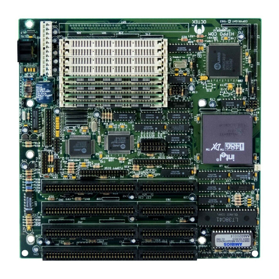
- Page 67 Appendix C System Board Layout ___________________________________________________________ _________________________________________________________________________...
Need help?
Do you have a question about the Hippo COM and is the answer not in the manual?
Questions and answers