
Related Manuals for Quectel AF50T

Summary of Contents for Quectel AF50T
- Page 1 AF50T Hardware Design Wi-Fi&BT Module Series Version: 1.0.1 Date: 2020-12-17 Status: Preliminary www.quectel.com...
- Page 2 To the maximum extent permitted by law, Quectel excludes all liability for any loss or damage suffered in connection with the use of the functions and features under development, regardless of whether such loss or damage may have been foreseeable.
- Page 3 AF50T Hardware Design Copyright The information contained here is proprietary technical information of Quectel wireless solutions co., ltd. Transmitting, reproducing, disseminating and editing this document as well as using the content without permission are forbidden. Offenders will be held liable for payment of damages. All rights are reserved in the event of a patent grant or registration of a utility model or design.
-
Page 4: About The Document
Wi-Fi&BT Module Series AF50T Hardware Design About the Document Revision History Version Date Author Description Jone CHEN/ 2019-11-25 Creation of the document Felix FU Jone CHEN/ 1.0.0 2019-11-25 Preliminary Felix FU Preliminary: Updated the key features (Table 1). Changed the name of pin 48, pin 60, pin 61, pin 3,... -
Page 5: Table Of Contents
Wi-Fi&BT Module Series AF50T Hardware Design Contents About the Document ..........................3 Contents ..............................4 Table Index ..............................6 Figure Index ..............................7 Introduction ............................8 1.1. Safety Information ........................9 Product Concept ..........................10 2.1. General Description ......................... 10 2.2. - Page 6 Wi-Fi&BT Module Series AF50T Hardware Design 4.2. Electrical Characteristics ......................34 4.3. I/O Interface Characteristics ....................35 4.4. Current Consumption ....................... 36 4.5. RF Performances ........................37 4.5.1. Conducted RF Performance of Wi-Fi ................37 4.5.2. Conducted RF Performance of Bluetooth ..............41 4.6.
- Page 7 Wi-Fi&BT Module Series AF50T Hardware Design Table Index Table 1: Key Features ..........................10 Table 2: I/O Parameters Definition ......................15 Table 3: Pin Description ..........................15 Table 4: Definition of Power Supply and GND Pins ................... 19 Table 5: Pin Definition of WLAN_EN ......................21 Table 6: Pin Definition of PCIe Interface ....................
- Page 8 Wi-Fi&BT Module Series AF50T Hardware Design Figure Index Figure 1: Functional Diagram of AF50T Module ..................12 Figure 2: Pin Assignment (Top View) ......................14 Figure 3: Reference Circuit for VDD_CORE_VL, VDD_CORE_VM, VDD_CORE_VH, and VDD_IO ..19 Figure 4: Reference Circuit for VDD_RF ....................20 Figure 5: WLAN Interface Connection .......................
-
Page 9: Introduction
Wi-Fi&BT Module Series AF50T Hardware Design Introduction This document defines the AF50T module and describes its air interface and hardware interfaces which are connected with customers’ applications. The document helps customers quickly understand module interface specifications, as well as the electrical and mechanical details. -
Page 10: Safety Information
Manufacturers of the cellular terminal should notify users and operating personnel of the following safety information by incorporating these guidelines into all manuals of the product. Otherwise, Quectel assumes no liability for customers’ failure to comply with these precautions. -
Page 11: Product Concept
WLAN and BT Low Energy technologies. AF50T supports a low-power PCIe Gen 2 interface for WLAN and a UART/PCM interface for BT, and also supports LTE & WLAN/BT coexistence interface. It is designed to be used in conjunction with Quectel 5G V2X module AG55xQ series to provide it with WLAN and BT functions. - Page 12 Wi-Fi&BT Module Series AF50T Hardware Design 2.4 GHz 802.11b/11 Mbps: 20 dBm 802.11g/54 Mbps: 16 dBm 802.11n/HT20 MCS7: 16 dBm 802.11n/HT40 MCS7: 16 dBm 802.11ax/HE20 MCS11: 14 dBm 802.11ax/HE40 MCS11: 14 dBm 5 GHz Transmitting Power 802.11a/54 Mbps: 15 dBm 802.11n/HT20 MCS7: 15 dBm...
-
Page 13: Functional Diagram
Figure 1: Functional Diagram of AF50T Module 2.4. Evaluation Board To help customers develop applications with AF50T module conveniently, Quectel supplies the evaluation board (EVB), USB to RS232 converter cable, USB data cable, power adapter, antenna and other peripherals to control or test the module. For more details, see document [1] and/or document [2]. -
Page 14: Application Interfaces
AF50T Hardware Design Application Interfaces 3.1. General Description AF50T module is equipped with 108 LGA pins that can be connected to the cellular application platform. The subsequent chapters will provide a detailed introduction to the following interfaces and pins of the module: ... -
Page 15: Pin Assignment
Wi-Fi&BT Module Series AF50T Hardware Design 3.2. Pin Assignment HOST_ WAKEUP_ PCM_SYNC WAKEUP_ PCM_DOUT HOST RESERVED PCM_DIN RESERVED PCM_CLK RESERVED BT_RTS VDD_RF BT_CTS VDD_RF BT_RXD VDD_RF BT_TXD RESERVED RESERVED RESERVED RESERVED RESERVED PA_MUTE RESERVED LAA_TXEN RESERVED LAA_RX WLAN_TXE COEX_RXD COEX_TXD... -
Page 16: Pin Description
Wi-Fi&BT Module Series AF50T Hardware Design 3.3. Pin Description The following tables show the pin description of AF50T module. Table 2: I/O Parameters Definition Type Description Analog Input Analog Output Digital Input Digital Output Bidirectional Power Input Table 3: Pin Description... - Page 17 Wi-Fi&BT Module Series AF50T Hardware Design WLAN Interface Pin Name Description DC Characteristics Comment min = -0.3 V WLAN function max = 0.63 V 1.8 V power domain. WLAN_EN enable control min = 1.17 V Active high. max = 2.1 V...
- Page 18 Wi-Fi&BT Module Series AF50T Hardware Design min = -0.3 V max = 0.63 V PCM_CLK* PCM clock 1.8 V power domain. min = 1.17 V max = 2.1 V max = 0.45 V PCM_DOUT* PCM data output 1.8 V power domain.
- Page 19 Wi-Fi&BT Module Series AF50T Hardware Design WLAN FEM during max = 0.63 V If unused, keep this WLAN sleep mode min = 1.17 V pin open. max = 2.1 V min = -0.3 V 1.8 V power domain. WLAN XFEM control max = 0.63 V...
-
Page 20: Power Supply
Please keep all RESERVED and unused pins open. “*” means under development. 3.4. Power Supply The following table shows the power supply pins and ground pins of AF50T module. Table 4: Definition of Power Supply and GND Pins Pin Name Pin No. -
Page 21: Wlan Interface
Wi-Fi&BT Module Series AF50T Hardware Design AF50T module is powered by VDD_RF, and it is recommended to use a power supply chip, which is able to output a current of 1.3 A at least. The following figure shows a reference design for VDD_RF which is controlled by WLAN_PWR_EN1 of AG55xQ series. -
Page 22: Wlan_En
WLAN function enable control Active high NOTE WLAN_EN is a sensitive signal, and it should be ground shielded and be routed as close to AF50T as possible. 3.5.2. PCIe Interface The following table shows the pin definition of the PCIe interface of AF50T. -
Page 23: Bt Interface
To ensure the signal integrity of PCIe interface, C1 and C2 should be placed close to the AG55xQ series module, and C3 and C4 should be placed close to the AF50T. The extra stubs of traces must be as short as possible. -
Page 24: Bt_En
AG55xQ series module. Figure 7: Block Diagram of BT Interface Connection 3.6.1. BT_EN BT_EN is used to control the BT function of AF50T module. BT function will be enabled when BT_EN is at high level. Table 7: Pin Definition of BT_EN Pin Name Pin No. -
Page 25: Uart Interface
1.8 V power domain BT_TXD BT UART transmit 1.8 V power domain BT_RXD BT UART receive 1.8 V power domain The following figure shows the reference design for UART interface connection between AF50T and AG55xQ series modules. AF50T_Hardware_Design 24 / 52... -
Page 26: Control Signal Pins
Active high. SW_CTRL Control PMIC outputs Under development. The following figure shows the reference design for SW_CTRL connection between AF50T and AG55xQ series modules. Figure 10: SW_CTRL Connection 3.7.2. HOST_WAKEUP_BT and BT_WAKEUP_HOST The following table shows the pin definition of HOST_WAKEUP_BT and BT_WAKEUP_HOST. -
Page 27: Coexistence Interfaces
Wi-Fi&BT Module Series AF50T Hardware Design These two pins are only used for AF50T + third-part host application. For AF50T + AG55xQ series application, they are not needed. Table 11: Pin Definition of HOST_WAKEUP_BT and BT_WAKEUP_HOST Pin Name Pin No. -
Page 28: Other Coexistence Interfaces
NOTE “*” means under development. 3.9. WLAN_SLP_CLK Interface An external 32.768 kHz sleep clock connecting to WLAN_SLP_CLK is necessary. AF50T is unable to boot up and work without sleep clock. Table 14: Pin Definition of WLAN_SLP_CLK Interface Pin Name Pin No. -
Page 29: Rf Antenna Interfaces
2.402–2.480 3.10.2. Reference Design of RF Antenna Interfaces AF50T module provides three RF antenna interfaces for antenna connection. A reference circuit design for an RF antenna interface is shown below. It is recommended to reserve a π-type and LCs matching circuit for better RF performance, and add a TVS for ESD protection. -
Page 30: Reference Design Of Rf Layout
Wi-Fi&BT Module Series AF50T Hardware Design Figure 12: Reference Circuit for RF Antenna Interfaces 3.10.3. Reference Design of RF Layout For user’s PCB, the characteristic impedance of all RF traces should be controlled to 50 Ω. The impedance of the RF traces is usually determined by the trace width (W), the materials’ dielectric constant, the height from the reference ground to the signal layer (H), and the spacing between RF traces and grounds (S). - Page 31 Wi-Fi&BT Module Series AF50T Hardware Design Figure 15: Coplanar Waveguide Design on a 4-layer PCB (Layer 3 as Reference Ground) Figure 16: Coplanar Waveguide Design on a 4-layer PCB (Layer 4 as Reference Ground) To ensure RF performance and reliability, the following principles should be complied with in RF layout design: ...
-
Page 32: Antenna Requirements
Wi-Fi&BT Module Series AF50T Hardware Design 3.10.4. Antenna Requirements The following tables show the requirements on antenna cables and antennas. Table 17: Antenna Cable Requirements Type Requirements 2.412–2.472 GHz Cable insertion loss <1 dB 5.180–5.825 GHz Cable insertion loss <1 dB... -
Page 33: Recommended Rf Connector For Antenna Installation
Wi-Fi&BT Module Series AF50T Hardware Design 3.10.5. Recommended RF Connector for Antenna Installation If RF connector is used for antenna connection, it is recommended to use U.FL-R-SMT connector provided by Hirose. Figure 17: Dimensions of the U.FL-R-SMT Connector (Unit: mm) U.FL-LP serial connectors listed in the following figure can be used to match the U.FL-R-SMT. - Page 34 Wi-Fi&BT Module Series AF50T Hardware Design The following figure describes the space factor of mated connector Figure 19: Space Factor of Mated Connector (Unit: mm) For more details, please visit http://www.hirose.com. AF50T_Hardware_Design 33 / 52...
-
Page 35: Reliability, Radio And Electrical Characteristics
AF50T Hardware Design Reliability, Radio and Electrical Characteristics 4.1. General Description This chapter mainly introduces electrical and radio frequency characteristics of AF50T module. The details are listed in the subsequent chapters. 4.2. Electrical Characteristics The following table shows the absolute maximum ratings. -
Page 36: I/O Interface Characteristics
Wi-Fi&BT Module Series AF50T Hardware Design The following table shows the recommended operating conditions of AF50T module. Table 20: Recommended Operating Conditions Parameter Min. Typ. Max. Unit VDD_CORE_VL 0.95 1.05 VDD_CORE_VM 1.28 1.35 1.42 VDD_CORE_VH 1.85 VDD_IO 1.71 1.89 VDD_RF 3.85... -
Page 37: Current Consumption
Wi-Fi&BT Module Series AF50T Hardware Design 4.4. Current Consumption The values of current consumption are shown as below. Table 22: Current Consumption of the Module (Normal Operation) VDD_ VDD_ VDD_ Description Conditions Unit VDD_IO VDD_RF CORE_VL CORE_VM CORE_VH TX 1 Mbps @ 20 dBm 217.67... -
Page 38: Rf Performances
TX HE80-MCS11 @ 12 dBm 306.87 143.34 77.80 3.79 198.52 4.5. RF Performances The following tables summarize the transmitting and receiving performances of AF50T. 4.5.1. Conducted RF Performance of Wi-Fi Table 23: Conducted RF Output Power at 2.4 GHz (SISO) Frequency Min. Typ. Max. - Page 39 Wi-Fi&BT Module Series AF50T Hardware Design 802.11ax, HE20 @ MCS11 802.11ax, HE40 @ MCS0 802.11ax, HE40 @ MCS11 Table 24: Conducted RF Output Power at 2.4 GHz (MIMO) Frequency Min. Typ. Max. Unit 802.11n, HT20 @ MCS0 802.11n, HT20 @ MCS7 802.11n, HT40 @ MCS0...
- Page 40 Wi-Fi&BT Module Series AF50T Hardware Design 802.11ac, VHT40 @ MCS0 802.11ac, VHT40 @ MCS9 802.11ac, VHT80 @ MCS0 802.11ac, VHT80 @ MCS9 802.11ax, HE20 @ MCS0 802.11ax, HE20 @ MCS11 802.11ax, HE40 @ MCS0 802.11ax, HE40 @ MCS11 802.11ax, HE80 @ MCS0 802.11ax, HE80 @ MCS11...
- Page 41 Wi-Fi&BT Module Series AF50T Hardware Design 802.11ax, HE40 @ MCS0 802.11ax, HE40 @ MCS11 802.11ax, HE80 @ MCS0 802.11ax, HE80 @ MCS11 Table 27: Conducted RF Receiving Sensitivity at 2.4 GHz Frequency Receiving Sensitivity (Typ.) 802.11b @ 1 Mbps -96 dBm 802.11b @ 11 Mbps...
-
Page 42: Conducted Rf Performance Of Bluetooth
Wi-Fi&BT Module Series AF50T Hardware Design 802.11n, HT20 @ MCS7 -74 dBm 802.11n, HT40 @ MCS0 -90 dBm 802.11n, HT40 @ MCS7 -72 dBm 802.11ac, VHT20 @ MCS0 -93 dBm 802.11ac, VHT20 @ MCS8 -71 dBm 802.11ac, VHT40 @ MCS0 -90 dBm 802.11ac, VHT40 @ MCS9... -
Page 43: Electrostatic Discharge
Wi-Fi&BT Module Series AF50T Hardware Design 4.6. Electrostatic Discharge The module is not protected against Electrostatic Discharge (ESD) in general. Consequently, it is subject to ESD handling precautions that typically apply to ESD sensitive components. Proper ESD handling and packaging procedures must be applied throughout the processing, handling and operation of any application that incorporates the module. -
Page 44: Mechanical Dimensions
Wi-Fi&BT Module Series AF50T Hardware Design Mechanical Dimensions This chapter describes the mechanical dimensions of AF50T module. All dimensions are measured in millimeter (mm), and the dimensional tolerances are ±0.05 mm unless otherwise specified. 5.1. Mechanical Dimensions of the Module... - Page 45 Wi-Fi&BT Module Series AF50T Hardware Design Figure 21: AF50T Bottom Dimension (Bottom View) NOTE The package warpage level of the module conforms to JEITA ED-7306 standard. AF50T_Hardware_Design 44 / 52...
-
Page 46: Recommended Footprint
Wi-Fi&BT Module Series AF50T Hardware Design 5.2. Recommended Footprint Figure 22: Recommended Footprint (Bottom View) NOTES 1. For easy maintenance of the module, please keep about 3mm spaces between the module and other components on host PCB. 2. Keep all RESERVED pins open. -
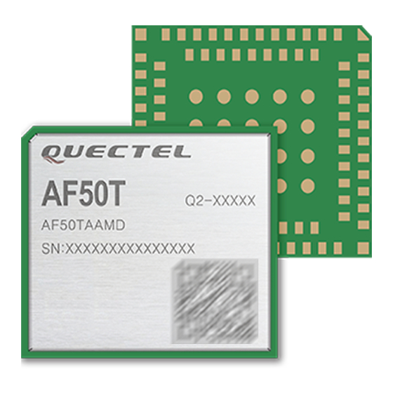
Page 47: Top And Bottom Views Of The Module
Figure 23: Top View of the Module Figure 24: Bottom View of the Module NOTE Images above are for illustration purpose only and may differ from the actual module. For authentic appearance and label, please refer to the module received from Quectel. AF50T_Hardware_Design 46 / 52... -
Page 48: Storage, Manufacturing And Packaging
Wi-Fi&BT Module Series AF50T Hardware Design Storage, Manufacturing and Packaging 6.1. Storage The module is provided with vacuum-sealed packaging. MSL of the module is rated as 3. The storage requirements are shown below. 1. Recommended Storage Condition: The temperature should be 23 ±5 °C and the relative humidity should be 35 %–60 %. -
Page 49: Manufacturing And Soldering
Wi-Fi&BT Module Series AF50T Hardware Design NOTES This floor life is only applicable when the environment conforms to IPC/JEDEC J-STD-033. 2. To avoid blistering, layer separation and other soldering issues, it is forbidden to expose the modules to the air for a long time. If the temperature and moisture do not conform to IPC/JEDEC J-STD-033 or the relative moisture is over 60 %, it is recommended to start the solder reflow process within 24 hours after the package is removed. -
Page 50: Packaging
6.3. Packaging AF50T module is packaged in a vacuum-sealed bag which is ESD protected. The bag should not be opened until the devices are ready to be soldered onto the application. AF50T is packaged in tape and reel carriers. - Page 51 Wi-Fi&BT Module Series AF50T Hardware Design Table 32: Reel Packaging Model Name MOQ for MP Minimum Package: TBD Minimum Package TBD Size: TBD Size: TBD AF50T N.W: TBD N.W: TBD G.W: TBD G.W: TBD AF50T_Hardware_Design 50 / 52...
-
Page 52: Appendix A References
Wi-Fi&BT Module Series AF50T Hardware Design Appendix A References Table 33: Related Documents Document Name Description EVB user guide for Quectel Quectel_LTE_OPEN_EVB_User_Guide LTE-QuecOpen modules Quectel_UMTS<E_EVB_User_Guide UMTS<E EVB user guide Quectel_AG55xQ_Series_QuecOpen_Reference_Design AG55xQ series reference design Quectel_RF_Layout_Application_Note RF layout application note Quectel_Module_Secondary_SMT_User_Guide... - Page 53 Wi-Fi&BT Module Series AF50T Hardware Design Long Term Evolution Mbps Megabits per second Modulation and Coding Scheme Minimum Order Quantity Printed Circuit Board Pulse Code Modulation Quadrature Amplitude Modulation QPSK Quadrature Phase Shift Keying Radio Frequency Relative Humidity RoHS Restriction of Hazardous Substances...
- Page 54 Wi-Fi&BT Module Series AF50T Hardware Design VSWR Voltage Standing Wave Ratio Wi-Fi Wireless-Fidelity WLAN Wireless Local Area Network FCC Certification Requirements. According to the definition of mobile and fixed device is described in Part 2.1091(b), this device is a mobile device.
- Page 55 Wi-Fi&BT Module Series AF50T Hardware Design The user’s manual or instruction manual for an intentional or unintentional radiator shall caution the user that changes or modifications not expressly approved by the party responsible for compliance could void the user's authority to operate the equipment. In cases where the manual is provided only in a form other...
Need help?
Do you have a question about the AF50T and is the answer not in the manual?
Questions and answers