
Subscribe to Our Youtube Channel
Related Manuals for ESD ECS-PCIe/FPGA


Summary of Contents for ESD ECS-PCIe/FPGA
- Page 1 ECS-PCIe/FPGA PCI Express® EtherCAT® Slave Interface ESC-PCIe/FPGA-LP (E.1106.04) Hardware Manual to Products E.1106.02, E.1106.04 ECS-PCIe/FPGA Hardware Manual Doc.-Nr.: E.1106.21 /-Rev 1.1 Page 1 of 28...
- Page 2 design.
- Page 3 2021-03-02 6.2, 6.3 Description of FPGA Type changed/corrected (Intel) Description of Pin Assignment of Connector X601 changed New Declaration of Conformity Technical details are subject to change without further notice. ECS-PCIe/FPGA Hardware Manual Doc.-Nr.: E.1106.21/ 1.1 Page 3 of 28...
- Page 4 This NOTICE statement contains the general mandatory sign and gives information that must be heeded and complied with for a safe use. INFORMATION INFORMATION Notes to point out something important or useful. Page 4 of 28 Hardware Manual Doc.-Nr.: E.1106.21 /Rev. 1.1 ECS-PCIe/FPGA...
-
Page 5: Safety Instructions
● The ECS-PCIe/FPGA may become warm during normal use. Always allow adequate ventilation around the ECS-PCIe/FPGA and use care when handling. ● Do not operate the ECS-PCIe/FPGA adjacent to heat sources and do not expose it to unnecessary thermal radiation. Ensure an ambient temperature as specified in the technical data. - Page 6 It is the responsibility of the device's user to take care that necessary safety precautions for the...
-
Page 7: Table Of Contents
7.2.2 X600 26 Pin Header configured for differential I/O ........... 25 7.3 X601 26 pin header for user I/O ..................26 7.4 JTAG FPGA (X1300) ......................26 8 Declaration of Conformity ......................27 9 Order Information ........................28 ECS-PCIe/FPGA Hardware Manual Doc.-Nr.: E.1106.21/ 1.1 Page 7 of 28... - Page 8 Figure 3: Installing ESI to EtherCAT Workbench (picture detail) ..........11 Figure 4: Scan result showing “Slave 1 (ECS-PCIe/FPGA)”, (picture detail) ........ 11 Figure 5: Process data view with “Slave 1 (ECS-PCIe/FPGA)”, (picture detail) ......12 Figure 6: Block circuit diagram ..................... 14 Figure 7: PCB top view of ECS-PCIe/FPGA-LP ................
-
Page 9: Quick Start
Quick Start 1 Quick Start This chapter describes first steps with the ECS-PCIe/FPGA. It uses an esd EtherCAT Slave Stack sample application and the esd EtherCAT Workbench to show the functionality of the ECS- PCIe/FPGA. 1.1 Requirements • EtherCAT knowledge. The ETG (EtherCAT Technology Group, http://ethercat.org) has several brochures/introductions that should be studied first •... -
Page 10: Driver Installation
64-bit Windows) and click Next: Figure 2: Update Driver Software 1.3.2 Linux The Linux driver for the esd EtherCAT slave device (ECS-PCIe/FPGA) is usually delivered as source code. Please refer to “.../driver/ECS-.../linux/README” from the extracted Slave Stack Linux archive. -
Page 11: Sample Slave Application
After the Workbench was (re)started a slave scan can be performed. Use the Online button to let the Workbench connect to its included Master and click the Scan button then: Figure 4: Scan result showing “Slave 1 (ECS-PCIe/FPGA)”, (picture detail) ECS-PCIe/FPGA Hardware Manual Doc.-Nr.: E.1106.21/ 1.1... -
Page 12: Figure 5: Process Data View With "Slave 1 (Ecs-Pcie/Fpga)", (Picture Detail)
Figure 5: Process data view with “Slave 1 (ECS-PCIe/FPGA)”, (picture detail) Double click the output (“Slave 1 (ECS-PCIe/FPGA).RxPDO1.Output1”) to write a new value to the slave. The Slave sample application shows the new value in its console output, for example: “[Application] *** output1 changed to 1234”... -
Page 13: Further Steps
EtherCAT Technology Group http:\\ethercat.org. This includes using your own EtherCAT vendor ID and testing the final product with the EtherCAT CTT (Conformance Test Tool). ECS-PCIe/FPGA Hardware Manual Doc.-Nr.: E.1106.21/ 1.1 Page 13 of 28... -
Page 14: Overview
CoE, FoE and EoE to communicate with this EtherCAT Slave device. Via pin header connectors equipped on the ECS-PCIe/FPGA 40 3.3 V LVTTL I/Os are available, including the signals from the EtherCAT slave controller: 2x Sync and 2x Latch for system synchronization. -
Page 15: Pcb View With Connectors
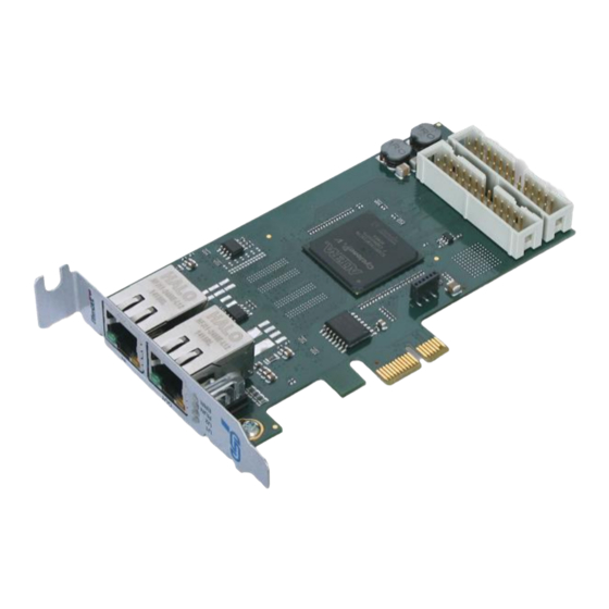
Read chapter “Hardware Installation” on page 18, before you start with the installation of the hardware! Figure 7 shows the low-profile version ECS-PCIe/FPGA-LP. The ECS-PCIe/FPGA only differs in the length of the slot bracket. See also page 23 for signal assignment of the CAN connectors. -
Page 16: Leds
LEDs 4 LEDs 4.1 Position of the LEDs Figure 8: Connectors and LEDs of ECS-PCIe/FPGA Figure 8 shows the ECS-PCIe/FPGA. The low-profile version ECS-PCIe/FPGA-LP only differs in the length of the slot bracket. 4.2 LED Indication Indicator states Description blinking LED blinking cycle: 200 ms on, 200 ms off. -
Page 17: Status Leds
FPGA and driver no Ethernet link Link/Activity Ethernet link is established, yellow port OUT blinking Ethernet Activity (Receiving Ethernet data packages) Table 3: Description of Link/Activity LEDs ECS-PCIe/FPGA Hardware Manual Doc.-Nr.: E.1106.21/ 1.1 Page 17 of 28... -
Page 18: Hardware Installation
Switch off your system and all connected peripheral devices (monitor, printer, etc.). Discharge your body as described above. Disconnect the system from the mains. Make sure that no risk arises from the system into which the ECS-PCIe/FPGA shall be inserted. DANGER... -
Page 19: Technical Data
Full-height: 120mm ECS-PCIe/FPGA-LP: Low-profile: 79,2mm Weight ECS-PCIe/FPGA: 80 g ECS-PCIe/FPGA-LP: 75 g Table 4: General data of the module 6.2 Hardware Components FPGA Intel Cyclone V GX up to 16 Mbyte – for active serial Boot Option Serial NOR FLASH... -
Page 20: Fpga
6.6 Temperature Sensor Number Type Texas Instruments TMP100 Accuracy / Resolution ±2.0°C from -25°C to 85°C / 9Bit Interface Controller Integrated in FPGA Table 9: Data of the temperature sensor Page 20 of 28 Hardware Manual Doc.-Nr.: E.1106.21 /Rev. 1.1 ECS-PCIe/FPGA... -
Page 21: Sync / Latch Interface
Controller Integrated in FPGA Power Supply 3,3V / 1A unprotected and 12V / 0,5A unprotected Output Table 12: Data of User-I/O interface on X601 ECS-PCIe/FPGA Hardware Manual Doc.-Nr.: E.1106.21/ 1.1 Page 21 of 28... -
Page 22: Software Support
The FPGA contains Bus Master DMA Support to offload the CPU from copying the output process image data into the host memory. This is utilized by the esd EtherCAT Slave Stack. Please refer to the EtherCAT Slave Stack manual (see “Order Information” page 28) for further information. -
Page 23: Connector Assignments
Permissible cable types: Cables of category 5 or higher must be used to grant the function in networks with up to 100 Mbits/s. esd grants the EC conformity of the product if the wiring is carried out with shielded twisted pair cables. -
Page 24: X600 26 Pin Header
The functions SYNC0, 1 and LATCH0, 1 are default on the pins shown. As an alternative function these pins can be switched to LVTTL_IO_xx independently for each pin as shown by register settings. Page 24 of 28 Hardware Manual Doc.-Nr.: E.1106.21 /Rev. 1.1 ECS-PCIe/FPGA... -
Page 25: X600 26 Pin Header Configured For Differential I/O
Output Output Diff Pair TX1-N Diff Pair RX1-P Input Input Diff Pair RX1-N Output Diff Pair TX0-N Diff Pair TX0-P Output Diff Pair RX0-P Input Input Diff Pair RX0-N 3,3V ECS-PCIe/FPGA Hardware Manual Doc.-Nr.: E.1106.21/ 1.1 Page 25 of 28... -
Page 26: X601 26 Pin Header For User I/O
LVTTL1_IO_9 LVTTL1_IO_10 LVTTL1_IO_11 Latch 2 Latch 3 Sync Out 2 Sync Out 3 3,3V LVTTL1_IO_12 LVTTL1_IO_13 LVTTL1_IO_14 LVTTL1_IO_15 3,3V 7.4 JTAG FPGA (X1300) Signal Direction Input Output Input Input Page 26 of 28 Hardware Manual Doc.-Nr.: E.1106.21 /Rev. 1.1 ECS-PCIe/FPGA... -
Page 27: Declaration Of Conformity
Declaration of Conformity 8 Declaration of Conformity ECS-PCIe/FPGA Hardware Manual Doc.-Nr.: E.1106.21/ 1.1 Page 27 of 28... -
Page 28: Order Information
P.4520.21 Table 14: Available manuals Printed Manuals If you need a printout of the manual additionally, please contact our sales team (sales@esd.eu) for a quotation. Printed manuals may be ordered for a fee. Page 28 of 28 Hardware Manual Doc.-Nr.: E.1106.21 /Rev. 1.1...
Need help?
Do you have a question about the ECS-PCIe/FPGA and is the answer not in the manual?
Questions and answers