Table of Contents
Advertisement
Quick Links
www.ti.com
User's Guide
TPS53915 Step-Down Converter Evaluation Module User's
Guide
1
Introduction.............................................................................................................................................................................2
2 Description..............................................................................................................................................................................
Applications............................................................................................................................................................2
2.2 Features.............................................................................................................................................................................
3 Electrical Performance Specifications.................................................................................................................................
4
Schematic................................................................................................................................................................................3
Setup................................................................................................................................................................................4
5.1 Test Equipment..................................................................................................................................................................
Setup.................................................................................................................................................5
6 Configurations........................................................................................................................................................................
Selection..................................................................................................................................................6
6.2 Mode Selection..................................................................................................................................................................
Selection..................................................................................................................................................6
7 Test Procedure........................................................................................................................................................................
7.1 Line and Load Regulation and Efficiency Measurement Procedure..................................................................................
7.2 PMBUS Setup and Verification..........................................................................................................................................
7.4 List of Test Points.............................................................................................................................................................
7.5 Equipment Shutdown.......................................................................................................................................................
8 EVM Assembly Drawing and PCB Layout..........................................................................................................................
9 Bill of Materials.....................................................................................................................................................................
10 Revision History.................................................................................................................................................................
Figure 4-1. TPS53915EVM-PWR587 Schematic........................................................................................................................
Figure 5-2. TPS53915EVM-587 Top Layer for Test Setup..........................................................................................................
Figure 7-1. Select Device Scanning Mode..................................................................................................................................
Figure 7-2. GUI for the Fusion Digital Power Designer.............................................................................................................
Figure 8-2. TPS53915EVM-587 Bottom-Layer Assembly Drawing...........................................................................................
Figure 8-3. TPS53915EVM-587 Top Layer, Copper..................................................................................................................
Figure 8-4. TPS53915EVM-587 Layer Two, Copper.................................................................................................................
Figure 8-5. TPS53915EVM-587 Layer Three, Copper..............................................................................................................
Figure 8-6. TPS53915EVM-587 Layer Four, Copper................................................................................................................
Figure 8-8. TPS53915EVM-587 Bottom Layer, Copper............................................................................................................
Table 6-1. PMBus Address Selection Settings............................................................................................................................
Table 6-2. Mode Selection...........................................................................................................................................................
Table 6-3. Enable Selection.........................................................................................................................................................
Table 7-1. Test Point Functions..................................................................................................................................................
Trademarks
D-CAP3
™
is a trademark of Texas Instruments.
All trademarks are the property of their respective owners.
SLUUAS2C - OCTOBER 2013 - REVISED NOVEMBER 2021
Submit Document Feedback
Table of Contents
Procedure.................................................................................................10
List of Figures
Ripple............................................................................................................4
Drawing.................................................................................................12
Copper.................................................................................................................15
List of Tables
Figure 4-1)...........................................................................16
TPS53915 Step-Down Converter Evaluation Module User's Guide
Copyright © 2021 Texas Instruments Incorporated
(1)
...........................................................................
Table of Contents
2
2
2
4
6
6
8
8
8
11
11
12
16
17
3
5
9
10
12
13
13
14
14
15
2
6
6
7
11
1
Advertisement
Table of Contents

Related Manuals for Texas Instruments TPS53915


Summary of Contents for Texas Instruments TPS53915
-
Page 1: Table Of Contents
™ is a trademark of Texas Instruments. All trademarks are the property of their respective owners. SLUUAS2C – OCTOBER 2013 – REVISED NOVEMBER 2021 TPS53915 Step-Down Converter Evaluation Module User's Guide Submit Document Feedback Copyright © 2021 Texas Instruments Incorporated... -
Page 2: Introduction
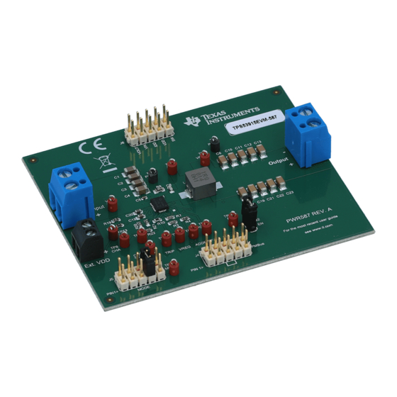
The TPS53915EVM-PWR587 is designed for a regulated 12-V bus to produce a regulated 1.2-V output at up to 12 A of load current. The TPS53915EVM-PWR587 is designed to demonstrate the TPS53915 device in a typical low-voltage application while providing a number of test points to evaluate the performance of the TPS53915 device. -
Page 3: Schematic
PIN 26 ALERT# AGND PGND PIN 27 GND1 GND1 PIN 28 GND2 GND2 Figure 4-1. TPS53915EVM-PWR587 Schematic SLUUAS2C – OCTOBER 2013 – REVISED NOVEMBER 2021 TPS53915 Step-Down Converter Evaluation Module User's Guide Submit Document Feedback Copyright © 2021 Texas Instruments Incorporated... -
Page 4: Test Setup
The minimum recommended wire size is 2× AWG number 14, with the total length of wire less than four feet (two feet output, two feet return). TPS53915 Step-Down Converter Evaluation Module User's Guide SLUUAS2C – OCTOBER 2013 – REVISED NOVEMBER 2021 Submit Document Feedback Copyright ©... -
Page 5: Recommended Test Setup
2. Connect the voltmeter V2 at TP7 (VOUT) and TP9 (GND) to measure the output voltage. SLUUAS2C – OCTOBER 2013 – REVISED NOVEMBER 2021 TPS53915 Step-Down Converter Evaluation Module User's Guide Submit Document Feedback Copyright © 2021 Texas Instruments Incorporated... -
Page 6: Configurations
The device enters FCCM after PGOOD goes high. 6.3 VDD Pin Supply Selection The controller can be enabled and disabled by J7. TPS53915 Step-Down Converter Evaluation Module User's Guide SLUUAS2C – OCTOBER 2013 – REVISED NOVEMBER 2021 Submit Document Feedback... -
Page 7: Table 6-3. Enable Selection
For power up, input J7 with proper voltage. The VDD pin input voltage range is from 4.5 V to 25 V. SLUUAS2C – OCTOBER 2013 – REVISED NOVEMBER 2021 TPS53915 Step-Down Converter Evaluation Module User's Guide Submit Document Feedback Copyright © 2021 Texas Instruments Incorporated... -
Page 8: Test Procedure
13. Click on Write to Hardware and monitor the change of the switching frequency on the oscilloscope. See the TPS53915 1.5 to 18 V (4.5 to 25 V bias) Input, 12-A Single Synchronous Step-Down SWIFT™ Converter Data Sheet for more information regarding PMBUS registers. -
Page 9: Figure 7-1. Select Device Scanning Mode
Test Procedure Figure 7-1. Select Device Scanning Mode SLUUAS2C – OCTOBER 2013 – REVISED NOVEMBER 2021 TPS53915 Step-Down Converter Evaluation Module User's Guide Submit Document Feedback Copyright © 2021 Texas Instruments Incorporated... -
Page 10: Control-Loop Gain And Phase-Measurement Procedure
7. Disconnect the isolation transformer from the bode-plot test points before making other measurements. • Signal injection into feedback can interfere with the accuracy of other measurements. TPS53915 Step-Down Converter Evaluation Module User's Guide SLUUAS2C – OCTOBER 2013 – REVISED NOVEMBER 2021 Submit Document Feedback... -
Page 11: List Of Test Points
Follow these steps when shutting down the equipment. 1. Shut down load 2. Shut down VIN SLUUAS2C – OCTOBER 2013 – REVISED NOVEMBER 2021 TPS53915 Step-Down Converter Evaluation Module User's Guide Submit Document Feedback Copyright © 2021 Texas Instruments Incorporated... -
Page 12: Evm Assembly Drawing And Pcb Layout
8-8). The EVM has been designed using a six-layer 2-oz copper-circuit board. Figure 8-1. TPS53915EVM-587 Top-Layer Assembly Drawing Figure 8-2. TPS53915EVM-587 Bottom-Layer Assembly Drawing TPS53915 Step-Down Converter Evaluation Module User's Guide SLUUAS2C – OCTOBER 2013 – REVISED NOVEMBER 2021 Submit Document Feedback... -
Page 13: Figure 8-3. Tps53915Evm-587 Top Layer, Copper
EVM Assembly Drawing and PCB Layout Figure 8-3. TPS53915EVM-587 Top Layer, Copper Figure 8-4. TPS53915EVM-587 Layer Two, Copper SLUUAS2C – OCTOBER 2013 – REVISED NOVEMBER 2021 TPS53915 Step-Down Converter Evaluation Module User's Guide Submit Document Feedback Copyright © 2021 Texas Instruments Incorporated... -
Page 14: Figure 8-5. Tps53915Evm-587 Layer Three, Copper
EVM Assembly Drawing and PCB Layout www.ti.com Figure 8-5. TPS53915EVM-587 Layer Three, Copper Figure 8-6. TPS53915EVM-587 Layer Four, Copper TPS53915 Step-Down Converter Evaluation Module User's Guide SLUUAS2C – OCTOBER 2013 – REVISED NOVEMBER 2021 Submit Document Feedback Copyright © 2021 Texas Instruments Incorporated... -
Page 15: Figure 8-7. Tps53915Evm-587 Layer Five
EVM Assembly Drawing and PCB Layout Figure 8-7. TPS53915EVM-587 Layer Five, Copper Figure 8-8. TPS53915EVM-587 Bottom Layer, Copper SLUUAS2C – OCTOBER 2013 – REVISED NOVEMBER 2021 TPS53915 Step-Down Converter Evaluation Module User's Guide Submit Document Feedback Copyright © 2021 Texas Instruments Incorporated... -
Page 16: Bill Of Materials
0.1 × 0.1 inch 5001 Keystone TPS53915RVE IC, High Performance, 12-A Single Sync. Step-Down Converter with PMBus. TPS53915RVE TPS53915 Step-Down Converter Evaluation Module User's Guide SLUUAS2C – OCTOBER 2013 – REVISED NOVEMBER 2021 Submit Document Feedback Copyright © 2021 Texas Instruments Incorporated... -
Page 17: Revision History
Changed the test points in the Tip and Barrel Measurement for VOUT Ripple image from TPS5 and TPS7 to TPS7 and TPS9 (respectively from left to right)....................SLUUAS2C – OCTOBER 2013 – REVISED NOVEMBER 2021 TPS53915 Step-Down Converter Evaluation Module User's Guide Submit Document Feedback Copyright © 2021 Texas Instruments Incorporated... - Page 18 STANDARD TERMS FOR EVALUATION MODULES Delivery: TI delivers TI evaluation boards, kits, or modules, including any accompanying demonstration software, components, and/or documentation which may be provided together or separately (collectively, an “EVM” or “EVMs”) to the User (“User”) in accordance with the terms set forth herein.
- Page 19 www.ti.com Regulatory Notices: 3.1 United States 3.1.1 Notice applicable to EVMs not FCC-Approved: FCC NOTICE: This kit is designed to allow product developers to evaluate electronic components, circuitry, or software associated with the kit to determine whether to incorporate such items in a finished product and software developers to write software applications for use with the end product.
- Page 20 www.ti.com Concernant les EVMs avec antennes détachables Conformément à la réglementation d'Industrie Canada, le présent émetteur radio peut fonctionner avec une antenne d'un type et d'un gain maximal (ou inférieur) approuvé pour l'émetteur par Industrie Canada. Dans le but de réduire les risques de brouillage radioélectrique à...
- Page 21 www.ti.com EVM Use Restrictions and Warnings: 4.1 EVMS ARE NOT FOR USE IN FUNCTIONAL SAFETY AND/OR SAFETY CRITICAL EVALUATIONS, INCLUDING BUT NOT LIMITED TO EVALUATIONS OF LIFE SUPPORT APPLICATIONS. 4.2 User must read and apply the user guide and other available documentation provided by TI regarding the EVM prior to handling or using the EVM, including without limitation any warning or restriction notices.
- Page 22 Notwithstanding the foregoing, any judgment may be enforced in any United States or foreign court, and TI may seek injunctive relief in any United States or foreign court. Mailing Address: Texas Instruments, Post Office Box 655303, Dallas, Texas 75265 Copyright © 2019, Texas Instruments Incorporated...
- Page 23 TI products. TI’s provision of these resources does not expand or otherwise alter TI’s applicable warranties or warranty disclaimers for TI products. TI objects to and rejects any additional or different terms you may have proposed. IMPORTANT NOTICE Mailing Address: Texas Instruments, Post Office Box 655303, Dallas, Texas 75265 Copyright © 2021, Texas Instruments Incorporated...
Need help?
Do you have a question about the TPS53915 and is the answer not in the manual?
Questions and answers