Table of Contents
Advertisement
Quick Links
www.ti.com
User's Guide
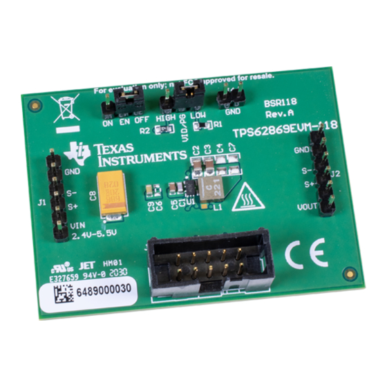
TPS62869EVM-118 Evaluation Module
This user's guide describes the characteristics, operation, and use of TI's evaluation module (EVM) for the
TPS628691, TPS628692, TPS628681, TPS628682 devices. The TPS62869EVM-118 (BSR118) facilitates the
evaluation of the TPS62869 family of 6-A, step-down converter with DCS-Control
QFN package solution. The EVM creates output voltages between 0.4V and 1.675V with 1% accuracy output
voltages from higher input voltages between 2.4 V and 5.5 V, to a regulated 0.9V output voltage. The TPS62869
family is a highly efficient and tiny solution for point-of-load (POL) converters for space-constrained applications,
such as artificial intelligence chips, camera modules, solid state drives (SSDs), and optical modules.
1
Introduction.............................................................................................................................................................................2
1.1 Performance Specification.................................................................................................................................................
1.2 Modifications......................................................................................................................................................................
2
Setup........................................................................................................................................................................................2
2.1 Input/Output Connector Descriptions.................................................................................................................................
2.2 Hardware Setup.................................................................................................................................................................
3 TPS62869EVM-118 Test Results............................................................................................................................................
Layout...........................................................................................................................................................................3
5 Schematic and List of Materials............................................................................................................................................
5.1 Schematic..........................................................................................................................................................................
5.2 List of Materials..................................................................................................................................................................
Interface..........................................................................................................................................................7
Setup...................................................................................................................................................................7
6.2 Interface Hardware Setup..................................................................................................................................................
Operation....................................................................................................................................................7
History......................................................................................................................................................................9
Figure 4-1. Top Assembly............................................................................................................................................................
Layer...................................................................................................................................................................3
Figure 4-3. Signal Layer 1...........................................................................................................................................................
Figure 4-4. Signal Layer 2...........................................................................................................................................................
Figure 4-5. Signal Layer 3...........................................................................................................................................................
Figure 4-6. Signal Layer 4...........................................................................................................................................................
Figure 4-7. Bottom Layer.............................................................................................................................................................
Figure 5-1. TPS62869EVM-118 Schematic.................................................................................................................................
Figure 6-1. Quick Connection Overview .....................................................................................................................................
Figure 6-2. GUI Home Screen.....................................................................................................................................................
Screen..................................................................................................................................................9
SLUUC88B - MARCH 2021 - REVISED NOVEMBER 2021
Submit Document Feedback
ABSTRACT
Table of Contents
List of Figures
List of Tables
Summary..........................................................................................................................2
Materials.............................................................................................................................6
Copyright © 2021 Texas Instruments Incorporated
Table of Contents
™
in a small 1.5-mm by 2.5-mm
TPS62869EVM-118 Evaluation Module
2
2
2
2
3
6
6
6
7
3
4
4
4
5
5
6
7
8
1
Advertisement
Table of Contents

Related Manuals for Texas Instruments TPS62869EVM-118


Summary of Contents for Texas Instruments TPS62869EVM-118
-
Page 1: Table Of Contents
TPS62869EVM-118 Evaluation Module ABSTRACT This user's guide describes the characteristics, operation, and use of TI's evaluation module (EVM) for the TPS628691, TPS628692, TPS628681, TPS628682 devices. The TPS62869EVM-118 (BSR118) facilitates the evaluation of the TPS62869 family of 6-A, step-down converter with DCS-Control ™... -
Page 2: Introduction
The printed-circuit board (PCB) for this EVM is designed to accommodate the different adjustable output voltage versions of this integrated circuit (IC). On the EVM, additional input and output capacitors can be added. 2 Setup This section describes how to properly use the TPS62869EVM-118. 2.1 Input/Output Connector Descriptions J1, Pin 1 and 2 – VIN Positive input connection from the input supply for the EVM J1, Pin 3 and 4 –... -
Page 3: Tps62869Evm-118 Test Results
TPS62869EVM-118 Test Results 3 TPS62869EVM-118 Test Results The TPS62869EVM-118 was used to take the typical characteristics in the TPS62869 data sheet (SLVSFS3). See the device data sheet for the performance of this EVM. 4 Board Layout This section provides the TPS62869EVM-118 board layout and illustrations in... -
Page 4: Figure 4-3. Signal Layer 1
Board Layout www.ti.com Figure 4-3. Signal Layer 1 Figure 4-4. Signal Layer 2 Figure 4-5. Signal Layer 3 TPS62869EVM-118 Evaluation Module SLUUC88B – MARCH 2021 – REVISED NOVEMBER 2021 Submit Document Feedback Copyright © 2021 Texas Instruments Incorporated... -
Page 5: Figure 4-6. Signal Layer 4
Board Layout Figure 4-6. Signal Layer 4 Figure 4-7. Bottom Layer SLUUC88B – MARCH 2021 – REVISED NOVEMBER 2021 TPS62869EVM-118 Evaluation Module Submit Document Feedback Copyright © 2021 Texas Instruments Incorporated... -
Page 6: Schematic And List Of Materials
Schematic and List of Materials www.ti.com 5 Schematic and List of Materials This section provides the TPS62869EVM-118 schematic and list of materials. 5.1 Schematic Figure 5-1 illustrates the EVM schematic. Figure 5-1. TPS62869EVM-118 Schematic 5.2 List of Materials Table 5-1 lists a list of materials for this EVM. -
Page 7: Software User Interface
The Home screen gives a short overview of the TPS62869 devices. To start evaluating the device, click on the Start button or on the Settings icons on the left side of the GUI window. SLUUC88B – MARCH 2021 – REVISED NOVEMBER 2021 TPS62869EVM-118 Evaluation Module Submit Document Feedback Copyright © 2021 Texas Instruments Incorporated... -
Page 8: Figure 6-2. Gui Home Screen
(if applicable). Refer to the register map in the TPS62869 2.4-V to 5.5-V Input, 6-A Synchronous Step-Down Converter Data Sheet for a detailed description of the TPS62869 registers. TPS62869EVM-118 Evaluation Module SLUUC88B – MARCH 2021 – REVISED NOVEMBER 2021 Submit Document Feedback Copyright © 2021 Texas Instruments Incorporated... -
Page 9: Revision History
Updated title from Setup to Hardware Setup ..................... Changes from Revision * (May 2021) to Revision A (March 2021) Page • Updated TPS62869EVM-118 Schematic......................6 SLUUC88B – MARCH 2021 – REVISED NOVEMBER 2021 TPS62869EVM-118 Evaluation Module Submit Document Feedback Copyright © 2021 Texas Instruments Incorporated... - Page 10 STANDARD TERMS FOR EVALUATION MODULES Delivery: TI delivers TI evaluation boards, kits, or modules, including any accompanying demonstration software, components, and/or documentation which may be provided together or separately (collectively, an “EVM” or “EVMs”) to the User (“User”) in accordance with the terms set forth herein.
- Page 11 www.ti.com Regulatory Notices: 3.1 United States 3.1.1 Notice applicable to EVMs not FCC-Approved: FCC NOTICE: This kit is designed to allow product developers to evaluate electronic components, circuitry, or software associated with the kit to determine whether to incorporate such items in a finished product and software developers to write software applications for use with the end product.
- Page 12 www.ti.com Concernant les EVMs avec antennes détachables Conformément à la réglementation d'Industrie Canada, le présent émetteur radio peut fonctionner avec une antenne d'un type et d'un gain maximal (ou inférieur) approuvé pour l'émetteur par Industrie Canada. Dans le but de réduire les risques de brouillage radioélectrique à...
- Page 13 www.ti.com EVM Use Restrictions and Warnings: 4.1 EVMS ARE NOT FOR USE IN FUNCTIONAL SAFETY AND/OR SAFETY CRITICAL EVALUATIONS, INCLUDING BUT NOT LIMITED TO EVALUATIONS OF LIFE SUPPORT APPLICATIONS. 4.2 User must read and apply the user guide and other available documentation provided by TI regarding the EVM prior to handling or using the EVM, including without limitation any warning or restriction notices.
- Page 14 Notwithstanding the foregoing, any judgment may be enforced in any United States or foreign court, and TI may seek injunctive relief in any United States or foreign court. Mailing Address: Texas Instruments, Post Office Box 655303, Dallas, Texas 75265 Copyright © 2019, Texas Instruments Incorporated...
- Page 15 TI products. TI’s provision of these resources does not expand or otherwise alter TI’s applicable warranties or warranty disclaimers for TI products. TI objects to and rejects any additional or different terms you may have proposed. IMPORTANT NOTICE Mailing Address: Texas Instruments, Post Office Box 655303, Dallas, Texas 75265 Copyright © 2021, Texas Instruments Incorporated...
Need help?
Do you have a question about the TPS62869EVM-118 and is the answer not in the manual?
Questions and answers