
Related Manuals for JYTEK PXIe-69852


Summary of Contents for JYTEK PXIe-69852
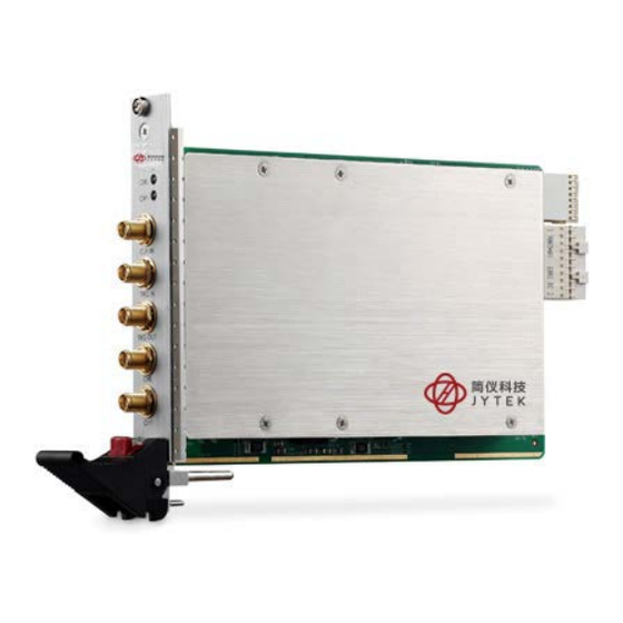
- Page 1 PXIe-69852 2-CH 14-Bit 200 MS/s Digitizer User’s Manual Manual Rev.: 1.00 Revision Date: Jul.16,2016...
-
Page 2: Getting Service
Getting Service Contact us should you require any service or assistance. SHANGHAI JYTEK Co., Ltd. Web site: http://www.jytek.com Address: 300 Fang Chun Rd., Zhangjiang Hi-Tech Park, Pudong New Area, Shanghai, 201203 China Tel: +86-21-5047-5899 Fax: +86-21-5047-5899 Email: service@jytek.com Additional information, aids, and tips that help users perform tasks Information to prevent minor physical injury, component damage, data loss, and/or program corruption when trying to complete a task. -
Page 3: Table Of Contents
Table of Contents Getting Service �������������������������������������������������������������������������������������������������������������� I 1 Introduction ������������������������������������������������������������������������������������������������������������ 1 1�1 Features ��������������������������������������������������������������������������������������������������������� 1 1.2 Applications ��������������������������������������������������������������������������������������������������� 1 1.3 Specifications ������������������������������������������������������������������������������������������������� 2 1�3�1 Analog Input ��������������������������������������������������������������������������������������� 2 1�3�2 Timebas ���������������������������������������������������������������������������������������������� 4 1�3�3 Triggers ����������������������������������������������������������������������������������������������� 4 1.3.4 General Specifications ������������������������������������������������������������������������� 5 1.4 Software Support �������������������������������������������������������������������������������������������... - Page 4 3.5.5 PXI_CLK100 Clock ������������������������������������������������������������������������������ 18 3�6 ADC Timing Control �������������������������������������������������������������������������������������� 19 3�6�1 Timebase Architecture ���������������������������������������������������������������������� 19 3.6.2 Basic Acquisition Timing �������������������������������������������������������������������� 19 3.7 Synchronizing Multiple Modules ������������������������������������������������������������������ 22 Appendix A Calibration ���������������������������������������������������������������������������������������������� 23 A.1 Calibration Constant ������������������������������������������������������������������������������������ 23 A.2 Auto-Calibration ������������������������������������������������������������������������������������������ 23 Important Safety Instructions �������������������������������������������������������������������������������������...
- Page 5 Table 1-3: Digital Trigger Input �������������������������������������������������������������������������������������� 4 Table 1-4: Digital Trigger Output ����������������������������������������������������������������������������������� 5 Table 1-5: PXIe-69852 I/O Array Legend ������������������������������������������������������������������������ 8 Table 3-1: Input Range and Data Format ��������������������������������������������������������������������� 12 Table 3-2: Input Range FSR and –FSR Values���������������������������������������������������������������� 12 Table 3-3: Input Range Midscale Values ����������������������������������������������������������������������...
- Page 6 Figure 1-3: PXIe-69852 Schematic ��������������������������������������������������������������������������������� 6 Figure 1-4: PXIe-69852 I/O Array ����������������������������������������������������������������������������������� 7 Figure 3-1: Analog Input Architecture of the PXIe-69852 ��������������������������������������������� 11 Figure 3-2: Linked List of PCI Address DMA Descriptors ����������������������������������������������� 13 Figure 3-3: Trigger Architecture of the PXIe-69852 ������������������������������������������������������ 13 Figure 3-4: External Digital Trigger ������������������������������������������������������������������������������...
-
Page 7: Introduction
1 Introduction The PXIe-69852 is a high-speed 2-CH 14-Bit 200 MS/s digitizer, specifically designed for applications such as LIDAR testing, optical fiber testing and radar signal acquisition. Analog input with 90MHz bandwidth receives ±10V high speed signals with 50Ω impedance, and a simplified front-end design and highly stable onboard reference provide both highly accurate measurement results and high dynamic performance. -
Page 8: Specifications
1�3 Specifications 1�3�1 Analog Input Channel Characteristics Comment Channels 2 single-ended Connector type Input coupling AC or DC, software selectable AC coupling cutoff frequency 11Hz ADC resolution 14-Bit Inout signal range ±0.2 V, ±2 V, or ±10 V Bandwidth(-3dB) 90MHz Overvoltage ±10V 1MΩ... -
Page 9: Figure 1-1: Analog Input Channel Bandwidth, ±0.2 Vpp
Bandwidth −1 −2 −3 −4 −5 −6 −7 −8 −9 0.1M 0.3M 100M 300M Frequency (Hz) Figure 1-1: Analog Input Channel Bandwidth, ±0.2 Vpp Bandwidth −1 −2 −3 −4 −5 −6 −7 −8 −9 0.1M 0.3M 100M 300M Frequency (Hz) Figure 1-2: Analog Input Channel Bandwidth, ±2 Vpp... -
Page 10: 1�3�2 Timebas
1�3�2 Timebas Sample Clock Comment Timebase options Internal : on board synthesizer External : CLK IN (front panel), PXI_CLK10, and PXIe_CLK100 Sampling clock frequency Internal : 200MHz 3.052kS/s to 200MS/s External : 40MHz ~ 200MHz (CLK IN) Timebase accuracy < ± 25ppm External reference clock source Front panel, PXI_CLK10, and PXIe_CLK100 External reference clock... -
Page 11: General Specifications
+3.3 V 12 V 1.4 Software Support JYTEK provides versatile software drivers and packages to suit various user approaches to building a system. Aside from programming libraries, such as DLLs, for most Windows-based systems, JYTEK also provides other drivers . -
Page 12: 1�4�1 Sdk
1�4�1 SDK For customers who want to write their own programs, JYTEK provides the following software development kits. • .NET driver for Windows, compatible with various application environments, such as C#, VB.NET, VC.NET, VB/VC++, BCB, and Delphi 1�4�2 WD-DASK WD-DASK includes device drivers and DLL for Windows XP/7/8. DLL is binary compatible across Windows XP/7/8. -
Page 13: Figure 1-4: Pxie-69852 I/O Array
The PXIe-69852 I/O array is labeled to indicate connectivity, as shown. Figure 1-4: PXIe-69852 I/O Array... -
Page 14: Table 1-5: Pxie-69852 I/O Array Legend
Timebase clock asserts Output and is output through this connector, at pulse width programmable from 50ns to 10μs via software Analog Analog input channel Input Analog Analog input channel Input Table 1-5: PXIe-69852 I/O Array Legend... -
Page 15: Getting Started
• Anti-static wrist strap • Antistatic mat JYTEK PXIe-69852 modules are electrostatically sensitive and can be easily damaged by static electricity. The module must be handled on a grounded anti-static mat. The operator must wear an anti-static wristband, grounded at the same point as the anti- static mat. -
Page 16: 2�2 Installing The Module
2�2 Installing the Module 1. Turn off the PXIe system/chassis and connect the power cable from the power source. Connection of the power cable provides grounding to prevent hazardous ESD (electrostatic discharge). 2. Align the module’s edge with the module guide in the PXIe chassis. 3. -
Page 17: Operations
3�2�2 Input Range and Data Format Data format of the PXIe-69852 is 2’s complement. The ADC data of PXIe-69852 is on the 14 MSB of the 16-bit A/D data. The 2 LSB of the 16-bit A/D data should be truncated by software. A/D data... -
Page 18: 3�2�3 Dma Data Transfer
Table 3-3: Input Range Midscale Values 3�2�3 DMA Data Transfer The PXIe-69852, a PCIe Gen 2 X 4 device, is equipped with a 200MS/s high sampling rate ADC, generating a 800 MByte/second rate. To provide efficient data transfer, a PCI bus-mastering DMA is essential for continuous data streaming, as it helps to achieve full potential PCI Express bus bandwidth. -
Page 19: 3�3 Trigger Source And Trigger Modes
3�3 Trigger Source and Trigger Modes This section details PXIe-69852 triggering operations. Figure 3-3: Trigger Architecture of the PXIe-69852 The PXIe-69852 requires a trigger to implement acquisition of data. Configuration of triggers requires identification of trigger source. The PXIe-69852 supports internal software trigger,... -
Page 20: Software Trigger
Figure 3-4: External Digital Trigger 3�3�3 PXI STAR Trigger When PXI STAR is selected as the trigger source, the PXIe-69852 accepts a TTL-compatible digital signal as a trigger signal. Triggering occurs when a rising edge or falling edge is detected at PXI STAR, with trigger polarity configurable by software. -
Page 21: Pxi Trigger Bus
When configured as input, the PXIe-69852 serves as a slave module and can accept trigger signals from one of buses 0 through 7. When configured as output, the PXIe-69852 serves as a master module and can output trigger signals to the PXI Trigger Bus Numbers 0 through 7. -
Page 22: 3�4�3 Pre-Trigger Mode
Figure 3-6: Delayed Trigger Mode Acquisition 3�4�3 Pre-Trigger Mode Collects data before the trigger event, starting once specified function calls are executed to begin the pre-trigger operation, and stopping when the trigger event occurs. If the trigger event occurs after the specified amount of data has been acquired, the system stores only data preceding the trigger event by a specified amount, as follows. -
Page 23: Acquisition With Re-Triggering
3.4.5 Acquisition with Re-Triggering A digitizer acquires a trace of N samples/channel for a single acquisition. Re-Trigger mode can also be set to automatically acquire R traces, containing N*R samples/channel of data, without additional software intervention. The Re-Trigger setting can be used for Post-Trigger and Delayed- Trigger modes, with different limitations on the spacing between trigger events in each mode. -
Page 24: 3�5 Timebase
200MHz clock for ADC. 3.5.2 External Reference Clock The PXIe-69852 can choose an external clock source for use as a reference clock. When an external clock reference is selected, the synthesizer input will switch to the clock source at SMA connector CLK IN, and generate precisely 200MHz clock for ADC. -
Page 25: 3�6 Adc Timing Control
Figure 3-11: PXIe-69852 Timebase Architecture 3.6.2 Basic Acquisition Timing The PXIe-69852 commences acquisition upon receipt of a trigger event originating with software command, external digital trigger, or the PXI Trigger Bus. The Timebase is a clock provided to the ADC and acquisition engine for essential timing. The Timebase is from an onboard synthesizer. To achieve different sampling rates, a scan interval counter is used. -
Page 26: Figure 3-12: Basic Digitizer Acquisition Timing
Analog signal TIMEBASE Trigger Acquisition Acquisition initiates following this clock edge In Progress D253 D254 D256 DATA Trigger mode = post-trigger, DataCnt = 256, ScanIntrv = 1 Figure 3-12: Basic Digitizer Acquisition Timing To achieve sampling rates other than 200MS/s, a number for scan interval counter needs only be specified. -
Page 27: Table 3-4: Counter Parameters And Description
Counter Name Length Valid Value Description ScanIntrv 16-bit 1-65535 Timebase divider to achieve equivalent sampling rate of the digitizer, where Sampling rate = Timebase / ScanIntrv DataCnt 28-bit 1-268435452 Specifies the amount of data to be acquired: • 1 - 268435452 for pre- trig or mid-trig mode operation •... -
Page 28: Synchronizing Multiple Modules
3�7 Synchronizing Multiple Modules The SSI (System Synchronization Interface) of the PXIe-69852 is achieved by a trigger signal, pre_ data_ready signal(s) and a reference clock, all transmitted through PXI_BUS ports to enable multiple module synchronization. When synchronizing multiple devices, a PXIe-69852 can be configured as a master or a slave, wherein the system accommodates multiple slave devices but only a single master device. -
Page 29: Appendix A Calibration
The PXIe-69852 is factory calibrated before shipment, with associated calibration constants written to the onboard EEPROM. At system boot, the PXIe-69852 driver loads these calibration constants, such that analog input path errors are minimized. JYTEK provides a software API for calibrating the PXIe-69852. -
Page 30: Important Safety Instructions
Important Safety Instructions For user safety, please read and follow all instructions, WARNINGS, CAUTIONS, and NOTES marked in this manual and on the associated equipment before handling/operating the equipment. • Read these safety instructions carefully. • Keep this user’s manual for future reference. •...
Need help?
Do you have a question about the PXIe-69852 and is the answer not in the manual?
Questions and answers