
Subscribe to Our Youtube Channel
Related Manuals for JYTEK PXIe-69834


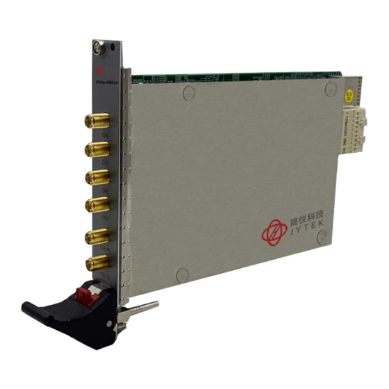
Summary of Contents for JYTEK PXIe-69834
- Page 1 PXIe-69834 4CH 16-bit 80MS/s PXIe Digitizer User’s Manual Manual Rev.: Revision Date: September 12, 2019 Part No: 50-17057-1000...
- Page 2 Revision History Revision Release Date Description of Change(s) September 12, 2019 Initial release...
- Page 3 Restriction of Hazardous Substances (RoHS) directive and Waste Electrical and Electronic Equipment (WEEE) directive. Environmental pro- tection is a top priority for JYTEK. We have enforced measures to ensure that our products, manufacturing processes, components, and raw materials have as little impact on the environment as possible.
- Page 4 Leading EDGE COMPUTING Battery Labels (for products with battery) California Proposition 65 Warning WARNING: This product can expose you to chemicals including acrylamide, arsenic, benzene, cadmium, Tris(1,3-dichloro-2-propyl) phosphate (TDCPP), 1,4- Dioxane, formaldehyde, lead, DEHP, styrene, DINP, BBP, PVC, and vinyl materials, which are known to the State of California to cause cancer, and acrylamide, benzene, cadmium, lead, mercury, phthalates, toluene, DEHP, DIDP, DnHP, DBP, BBP, PVC, and vinyl materials, which are known to the State of California to cause...
- Page 5 Conventions Take note of the following conventions used throughout this manual to make sure that users perform certain tasks and instructions properly. Additional information, aids, and tips that help users perform tasks. NOTE: NOTE: Information to prevent minor physical injury, component dam- age, data loss, and/or program corruption when trying to com- plete a task.
- Page 6 Leading EDGE COMPUTING This page intentionally left blank. Preface...
-
Page 7: Table Of Contents
Table of Contents Preface ..................iii List of Figures ................ ix List of Tables................xi 1 Introduction ................ 1 Features................1 Applications ................. 2 Specifications............... 2 1.3.1 Analog Input ............... 2 1.3.2 Accuracy..............3 1.3.3 System Noise ............. 3 1.3.4 Crosstalk, DC to 10MHz .......... - Page 8 Leading EDGE COMPUTING Functional Block Diagram ..........23 Analog Input Channel ............23 3.2.1 Analog Input Front-End Configuration ...... 23 3.2.2 Input Range and Data Format ........24 3.2.3 DMA Data Transfer........... 26 Trigger Source ..............27 3.3.1 Software Trigger ............28 3.3.2 External Digital Trigger ..........
-
Page 9: List Of Figures
Typical Frequency Response, 50Ω input impedance . 5 JYTEK MAPS Architecture ........10 Figure 1-3: JYTEK Connection Explorer (ACE) ......12 Figure 1-4: JYTEK Connection Explorer Soft Front Panel ..13 Figure 1-5: Figure 1-6: PXIe-69834 Dimensions........... 15 Figure 1-7: PXIe-69834 Front Panel ........... - Page 10 Leading EDGE COMPUTING This page intentionally left blank. List of Figures...
-
Page 11: List Of Tables
Table 1-11: Onboard Reference (Calibration)........8 Table 1-12: Specifications..............9 Table 1-13: Power Consumption ............9 Table 1-14: PXIe-69834 I/O Array Legend ........17 Table 3-1: Input Range and Data Format ........24 Table 3-2: Input Range FSR and -FSR Values....... 25 Table 3-3: Input Range Midscale Values ........ - Page 12 Leading EDGE COMPUTING This page intentionally left blank. List of Tables...
-
Page 13: Introduction
The PXIe-69834 features flexible input, ±10V (only for 1MΩ), ±5V,±1V and ±0.5V along with software selectable 50Ω or 1MΩ input impedance. Four high resolution 16-bit A/D converters combined with low-noise, high bandwidth analog front-end enable highly accurate signal acquisition. -
Page 14: Applications
Leading EDGE COMPUTING 1.2 Applications Testing/monitoring for Energy Management applications, including: Partial discharge Power line/device monitoring Non-destructive testing Radar acquisition LiDAR 1.3 Specifications 1.3.1 Analog Input Item Specification Comment Channels 4 single-ended Connector type Input DC or AC, software selectable coupling 16-Bit resolution... -
Page 15: Accuracy
1.3.2 Accuracy Offset Error Input Gain Error 50Ω Input 1MΩ Input Range Impedance Impedance ±0.5V ±0.8mV ±0.8mV ±1V ±0.8mV ±1.2mV ±0.6% ±5V ±1.5mV ±4.0mV ±10V ±8mV Table 1-2: Accuracy 1.3.3 System Noise Input Range System Noise 0.1mV ±0.5V 0.15mV ±1V ±5V 1.5mV ±10V... -
Page 16: Spectral Characteristics
Leading EDGE COMPUTING 1.3.5 Spectral Characteristics Index Specification Comment 68dB ±0.5V, ±1V, ±5V SINAD 65dB ±10V -78dB For all ranges SFDR 78dB For all ranges 69dB ±0.5V, ±1V, ±5V 65dB ±10V Values reflect 50Ω and 1MΩ input impedance with digital filter off. -
Page 17: Figure 1-2: Typical Frequency Response, 50Ω Input Impedance
Figure 1-2: Typical Frequency Response, 50Ω input impedance Introduction... -
Page 18: Timebase
Leading EDGE COMPUTING 1.3.6 Timebase Sample Clock Detail Comment Internal: Onboard oscillator External: CLK IN (front panel SMA connector) External reference clock: CLK IN (front Timebase options panel SMA con- The reference clock nector) supplies an onboard PLL circuit and generates PXI_10M (PXIe 80MHz for ADC. -
Page 19: Triggers
External Reference Specification Clock 0.45V to 5V Clock input range Clock input coupling Clock input impedance 50Ω Duty cycle tolerance 45% to 55% Reference clock 10MHz ± 2KHz frequency range Table 1-8: External Reference Clock 1.3.7 Triggers Trigger Source & Mode Internal: software trigger External: External digital trigger from TRG IN (front panel) -
Page 20: Table 1-10: External Digital Trigger Input
Leading EDGE COMPUTING External Digital Trigger Input Sources TRG IN, front panel SMA connector Compatibility 3.3 V TTL, 5 V tolerant Input high threshold (VIH) 2.0 V Input low threshold (VIL) 0.8 V Maximum input overload -0.5 V to +5.5 V Trigger polarity Rising or falling, software selectable Trigger pulse width... -
Page 21: Mechanical And Environmental
1.3.8 Mechanical and Environmental Item Specification Comment 3U, one-slot, PXI Dimensions 165mm (W) x 100mm (H) (PCB) Express module Bus Interface PCI Express x4 Gen1 Temperature: 0°C to 50°C Operating Relative humidity: 5% to 95%, non- Conditions condensing Temperature: -20°C to 80°C Storage Conditions Relative humidity: 5% to 95%, non- condensing... -
Page 22: Software Support
Leading EDGE COMPUTING 1.4 Software Support JYTEK provides versatile software drivers and packages to suit various user approaches to building a system. Aside from pro- gramming libraries, such as DLLs, for most Windows-based sys- tems, JYTEK also provides drivers for other application environments. -
Page 23: Maps Core
1.4.1 MAPS Core JYTEK MAPS Core is a software package that includes all the device drivers for Windows and a system level management tool called (JYTEK Connection Explorer). With MAPS Core installed in a user-provided PC, the operating system can... -
Page 24: Figure 1-4: Jytek Connection Explorer (Ace)
Leading EDGE COMPUTING MAPS Core also comes with a system management portal called JYTEK Connection Explorer (ACE). Through ACE, users can dis- cover and manage JYTEK DAQ modules. For example, the user can reserve a certain size of memory buffer for DMA operation. -
Page 25: Figure 1-5: Jytek Connection Explorer Soft Front Panel
By clicking the Launch but- ton in the lowest "Utility" block, this soft-front panel allows users to control digitizers through the UI and display the acquired wave- form/data on the screen. Figure 1-5: The JYTEK Connection Explorer (ACE) Soft Front Panel Introduction... -
Page 26: Maps/C, C & C++ Support
C/C++, such as header files, device API library and versatile sample programs for understanding how to manipulate the device correctly. Find the latest MAPS/C on the JYTEK web- site. Introduction... -
Page 27: Device Layout And I/O Connectors
1.5 Device Layout and I/O Connectors All dimensions are in mm. Figure 1-6: PXIe-69834 Dimensions Introduction... -
Page 28: Figure 1-7: Pxie-69834 Front Panel
Leading EDGE COMPUTING The PXIe-69834 I/O array is labeled to indicate connectivity, as shown. All I/O connectors are SMA. CLK IN TRG IN Figure 1-7: PXIe-69834 Front Panel Introduction... -
Page 29: Table 1-14: Pxie-69834 I/O Array Legend
Analog Input Channel Analog Analog Input for reference clock to the digitizer reference clock CLK IN External digital trigger input, receiving External Digital TRG IN trigger signal from external instrument, Trigger thus initiating acquisition Table 1-14: PXIe-69834 I/O Array Legend Introduction... - Page 30 Leading EDGE COMPUTING This page intentionally left blank. Introduction...
-
Page 31: Getting Started
Flat-head screwdriver Anti-static wrist strap Antistatic mat The JYTEK PXIe-69834 is electrostatically sensitive and can be easily damaged by static electricity. The module must be handled on a grounded anti-static mat. The operator must wear an anti-static wristband, grounded at the same point as the anti- static mat. -
Page 32: Package Contents
If any of these items are missing or damaged, contact the dealer. Do not install or apply power to equipment that is damaged or missing components. Retain the shipping carton and packing materials for inspection. Please contact your JYTEK dealer/ WARNING: vendor immediately for assistance and obtain authorization before returning any product. -
Page 33: Installing The Module
2.3 Installing the Module The power cable provides grounding to prevent hazardous ESD (electrostatic discharge). NOTE: NOTE: Do not to perform "hot swapping", replacement, disconnecting or connecting of any components (including cards and cabling) on chassis while the system is powered up. By not observing WARNING: this Warning, system damage and/or data loss, and physical injury (due to possible shock hazard) may result. - Page 34 Leading EDGE COMPUTING This page intentionally left blank. Getting Started...
-
Page 35: Operations
(x1 or x2) Channel 16 Bits FPGA Figure 3-2: Analog Input Architecture The PXIe-69834's 50Ω or 1MΩ input impedance circuit, along with AC/DC coupling, makes it easy to acquire a wide variety of signals. Sophisticated attenuation circuit design offers several Operations... -
Page 36: Input Range And Data Format
“Calibration” on page 45. 3.2.2 Input Range and Data Format Data format of the PXIe-69834 is 2’s complement. D15 to D0 bits represent the 16-bit data from ADC (2’s complement) Table 3-1: Input Range and Data Format Operations... -
Page 37: Table 3-2: Input Range Fsr And -Fsr Values
The following table shows the represented digital code when input voltage is at negative full scale and positive full scale. Since the data format for the PXIe-69834 is 2’s complement, the most signifi-cant bit represents the sign of input voltage. -
Page 38: Dma Data Transfer
Leading EDGE COMPUTING 3.2.3 DMA Data Transfer The PXIe-69834, a PXIe Gen 1 X 4 device, is equipped with four 80MS/s high sampling rate ADCs, generating a 640 MByte/ second rate. To provide efficient data transfer, a PCI bus-mastering DMA is essential for continuous data streaming, as it helps to achieve full potential PCI Express bus bandwidth. -
Page 39: Trigger Source
PXI Trigger Bus PXIe_DSTARB Figure 3-4: Trigger Architecture The PXIe-69834 requires a trigger to implement acquisition of data. Configuration of triggers requires identification of trigger sources. The PXIe-69834 supports internal software trigger, external digital trigger, analog trigger from AI CH0 to CH3, PXI Trigger Bus [0..7],... -
Page 40: Software Trigger
Leading EDGE COMPUTING PXI Star and PXIe differential star (PXIe_DSTARB). The trigger decision sends a trigger signal to internal FPGA for acquisition operation, as well as one of the PXI Trigger Bus bit for multi-mod- ule synchronization operations. 3.3.1 Software Trigger The software trigger, generated by software command, is asserted immediately following execution of specified function calls to begin the operation. -
Page 41: Analog Trigger
3.3.3 Analog Trigger An analog trigger is generated when one of AI input signal CH0 to CH3 meets the trigger condition. The trigger conditions for analog triggers as shown in Figure 3-6. Rising Edge Trigger This trigger event occurs when the analog input signal changes from a voltage lower than the specified trigger level to one higher than the specified trigger level. -
Page 42: Pxi Trigger Bus
The interconnected bus provided by PXI Trigger Bus supports easy synchronization of multiple modules. When configured as input, the PXIe-69834 serves as a slave mod-ule and will wait to commence signal acquisition until receiving a trigger from the PXI Trigger Bus. When configured as output, the PXIe-69834 serves as a master module and can output trigger to one of the PXI Trigger Bus. -
Page 43: Trigger Modes
Post-trigger acquisition is applicable when data is to be collected after the trigger event, as shown. When the operation starts, PXIe-69834 waits for a trigger event. Once the trigger signal is received, acquisition begins. Data is generated from ADC and transferred to system memory continuously. -
Page 44: Delayed Trigger Mode
Leading EDGE COMPUTING 3.4.2 Delayed Trigger Mode Delayed-trigger acquisition is utilized to postpone data collection after the trigger event, as shown. When the PXIe-69834 receives a trigger event, time delay implemented before commencing acquisition. The delay is specified by a 16-bit... -
Page 45: Middle Trigger Mode
3.4.4 Middle Trigger Mode Collects data before and after the trigger event, with the amount to be collected set individually (M and N samples), as follows Operation start Acquisition stop Trigger event occurs Acquisition start Data transfer to system begins Time Trigger Data... -
Page 46: Acquisition With Re-Triggering
Leading EDGE COMPUTING 3.4.5 Acquisition with Re-Triggering A digitizer acquires a trace of N samples/channel for a single acquisition. Re-Trigger mode can also be set to automatically acquire R traces, containing N*R samples/channel of data, without additional software intervention. The Re-Trigger setting can be used for Post-Trigger and Delayed- Trigger modes, with different limitations on the spacing between trigger events in each mode. -
Page 47: Timebase
3.5 Timebase Onboard Oscillator ADC 0 ADC 1 ADC 2 ADC 3 Phase Lock Buffer PXI_CLK10 Loop Figure 3-12: Timebase Architecture 3.5.1 Internal Sampling Clock The PXIe-69834 internal 80MHz crystal oscillator acts as a sam-pling clock for ADC. Operations... -
Page 48: External Reference Clock
Leading EDGE COMPUTING 3.5.3 External Reference Clock The onboard phase-lock loop (PLL) circuit allows the PXIe-69834 to synch to an external 10MHz reference, in situation where multi-module synchronization in the timebase is needed. By software command, the CLK IN will route external 10MHz clock to the PLL synthesizer and generate a precise 80MHz clock for ADC. -
Page 49: Acquisition Timing Control
3.6 Acquisition Timing Control The PXIe-69834 commences acquisition upon receipt of a trigger event originating with software command, external digital trigger, analog trigger, PXI_STAR, Trigger Bus, PXIe_DSTARB. Trigger mode allows collection of data when the trigger event occurs, depending trigger mode type. -
Page 50: Table 3-4: Counter Parameters And Description
Leading EDGE COMPUTING To achieve sampling rates other than 80MS/s, the scan interval counter (ScanIntrv) needs to be specified. For example, if the scan interval counter is set to 2, the equivalent sampling rate is 80MS/s/2=40MS/s. If 3, the equivalent sampling rate is 80MS/s/3= 26.66MS/s, and vice versa. -
Page 51: Synchronizing Multiple Modules
Digitizer modules such as the PXIe-69834 support trigger synchro-nization and timebase synchronization. Trigger synchronization implements a signal that initiates acquisi- tion, and timebase synchronization provides the fundamental clock for AD operation. -
Page 52: Figure 3-15: External Instrument Synchronization
Leading EDGE COMPUTING With appropriate configuration of digitizer modules and effective instrument support, however, trigger or timebase synchronization, or both can be achieved, commensurate with application require- ments. As shown in the following, in a simple synchronization architec- ture, two digitizer modules receive trigger and timebase from a function generator. -
Page 53: Figure 3-16: Module-Based Synchronization
Some digitizer modules provide advanced features that can output trigger or timebase to external devices, enabling multi-module synchronization as well. As shown in the following, digitizer #1 acts as a master device and transmits trigger/timebase to the two slave digitizers. TRG OUT CLK#1 CLK OUT... -
Page 54: Figure 3-17: Pxie Instrumentation Signals
Leading EDGE COMPUTING to maximize signal quality. Moreover, signal wiring must be pre- cisely deployed to minimize timing skew. PXIe-69834, based Express & specifications, enables trigger and clock signals to be fully leveraged and benefits from the routing architecture of the PXI Express chassis. -
Page 55: Multi-Module Synchronization Interfaces
PXI Trigger Bus, PXI_STAR, and PXIe_DSTARB are from the PXIe chassis. When the PXIe-69834 acts as a master device, its trigger signal is output to one bit of the PXI Trigger Bus, as determined by software selec-tion. -
Page 56: Figure 3-19: Pxi_Clk10 As 10Mhz Reference
Leading EDGE COMPUTING For timebase synchronization, the PXIe-69834 acts as a slave device, receiving 10MHz reference clock from the front panel CLK IN or PXI_CLK10 from the PXIe chassis. Onboard Oscillator ADC 0 ADC 1 ADC 2 ADC 3 Buffer... -
Page 57: A Appendix: Calibration
The PXIe-69834 is factory calibrated before shipment, with associ-ated calibration constants written to the onboard EEPROM. At system boot, the PXIe-69834 driver loads these calibration con-stants, such that analog input path errors are minimized. JYTEK provides a software API for calibrating the PXIe-69834. -
Page 58: Auto-Calibration
Auto-calibration can measure and minimize errors without external signal connections, reference voltages, or mea- surement devices. The PXIe-69834 has an on-board calibration reference to ensure the accuracy of auto-calibration. The reference voltage is mea-sured on the production line and recorded in the on-board EEPROM. -
Page 59: Figure A-2: Auto-Calibration Flow
Auto-calibration start Set analog front end input Set calibration source to onboard calibration source to calibration voltage Capture data and Set calibration source calculate gain to ground compensation parameters Capture data and calculate offset compensation Are all channels and parameters all ranges complete? Are all channels and all ranges complete? - Page 60 Leading EDGE COMPUTING This page intentionally left blank. Calibration...
-
Page 61: Important Safety Instructions
Important Safety Instructions For user safety, please read and follow all instructions, Warnings, Cautions, and Notes marked in this manual and on the associated device before handling/operating the device, to avoid injury or damage. S'il vous plaît prêter attention stricte à tous les avertissements et mises en garde figurant sur l'appareil , pour éviter des blessures ou des dommages. - Page 62 Leading EDGE COMPUTING Never attempt to repair the device, which should only be serviced by qualified technical personnel using suitable tools A Lithium-type battery may be provided for uninterrupted backup or emergency power. Risk of explosion if battery is replaced with one of an incorrect type;...
- Page 63 BURN HAZARD Touching this surface could result in bodily injury. To reduce risk, allow the surface to cool before touching. RISQUE DE BRÛLURES Ne touchez pas cette surface, cela pourrait entraîner des blessures. Pour éviter tout danger, laissez la surface refroidir avant de la toucher.
- Page 64 Leading EDGE COMPUTING This page intentionally left blank. Important Safety Instructions...
Need help?
Do you have a question about the PXIe-69834 and is the answer not in the manual?
Questions and answers