Sign In
Upload
Manuals
Brands
JYTEK Manuals
Measuring Instruments
PCIe-69852
JYTEK PCIe-69852 High-Speed Digitizer Manuals
Manuals and User Guides for JYTEK PCIe-69852 High-Speed Digitizer. We have
1
JYTEK PCIe-69852 High-Speed Digitizer manual available for free PDF download: User Manual
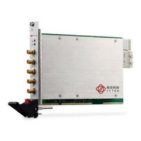
JYTEK PCIe-69852 User Manual (30 pages)
2-CH 14-Bit 200 MS/s Digitizer
Brand:
JYTEK
| Category:
Measuring Instruments
| Size: 1 MB
Table of Contents
Getting Service
2
Table of Contents
3
Introduction
7
1�1 Features
7
Applications
7
Specifications
8
1�3�1 Analog Input
8
Figure 1-1: Analog Input Channel Bandwidth, ±0.2 Vpp
9
Figure 1-2: Analog Input Channel Bandwidth, ±2 Vpp
9
1�3�2 Timebas
10
1�3�3 Triggers
10
Table 1-1: Timebase
10
Table 1-2: Trigger Source & Mode
10
Table 1-3: Digital Trigger Input
10
General Specifications
11
Software Support
11
Table 1-4: Digital Trigger Output
11
1�4�1 Sdk
12
1�4�2 Wd-Dask
12
1�5 Device Layout and I/O Array
12
Figure 1-3: Pxie-69852 Schematic
12
Figure 1-4: Pxie-69852 I/O Array
13
Table 1-5: Pxie-69852 I/O Array Legend
14
Getting Started
15
Installation Environment
15
2�2 Installing the Module
16
Operations
17
Functional Block Diagram
17
3�2 Analog Input Channel
17
Analog Input Front-End Configuration
17
3�2�2 Input Range and Data Format
17
Figure 3-1: Analog Input Architecture of the Pxie-69852
17
3�2�3 DMA Data Transfer
18
Table 3-1: Input Range and Data Format
18
Table 3-2: Input Range FSR and -FSR Values
18
Table 3-3: Input Range Midscale Values
18
3�3 Trigger Source and Trigger Modes
19
Figure 3-2: Linked List of PCI Address DMA Descriptors
19
Figure 3-3: Trigger Architecture of the Pxie-69852
19
3�3�3 PXI STAR Trigger
20
External Digital Trigger
20
Figure 3-4: External Digital Trigger
20
Pxie_Dstarb Trigger
20
Software Trigger
20
3�3�6 Analog Trigger
21
PXI Trigger Bus
21
Trigger Export
21
3�4 Trigger Modes
21
3�4�1 Post Trigger Mode
21
3�4�2 Delayed Trigger Mode
21
Figure 3-5: Post-Trigger Acquisition
21
3�4�3 Pre-Trigger Mode
22
3�4�4 Middle Trigger Mode
22
Figure 3-6: Delayed Trigger Mode Acquisition
22
Figure 3-7: Pre-Trigger Mode Acquisition
22
Figure 3-8: Middle Trigger Mode Acquisition
22
Acquisition with Re-Triggering
23
3�4�6 Data Average Mode (Post-Trigger and Delayed- Trigger Only)
23
Figure 3-9: Re-Trigger Mode Acquisition
23
3�5 Timebase
24
Internal Reference Clock
24
External Reference Clock
24
External Sampling Clock
24
PXI_CLK10 Clock
24
PXI_CLK100 Clock
24
Figure 3-10: Pxie-69852 Clock Architecture
24
3�6 ADC Timing Control
25
3�6�1 Timebase Architecture
25
Basic Acquisition Timing
25
Figure 3-11: Pxie-69852 Timebase Architecture
25
Figure 3-12: Basic Digitizer Acquisition Timing
26
Figure 3-13: Varying Sampling Rates by Adjusting Scan Interval Counter
26
Table 3-4: Counter Parameters and Description
27
Synchronizing Multiple Modules
28
Appendix A Calibration
29
Calibration Constant
29
Auto-Calibration
29
Important Safety Instructions
30
Advertisement
Advertisement
Related Products
JYTEK PCIe-69814 Series
JYTEK PCIe-69814P
JYTEK PCIe-69834
JYTEK PCIe-69834P
JYTEK PCI-69846D
JYTEK PCI-69816H
JYTEK PCI-69826H
JYTEK PCI-69846H
JYTEK PXIe-69834
JYTEK PXIe-69852
JYTEK Categories
Computer Hardware
Control Unit
Controller
Measuring Instruments
Chassis
More JYTEK Manuals
Login
Sign In
OR
Sign in with Facebook
Sign in with Google
Upload manual
Upload from disk
Upload from URL