
Related Manuals for JYTEK PXI-69816D


Summary of Contents for JYTEK PXI-69816D
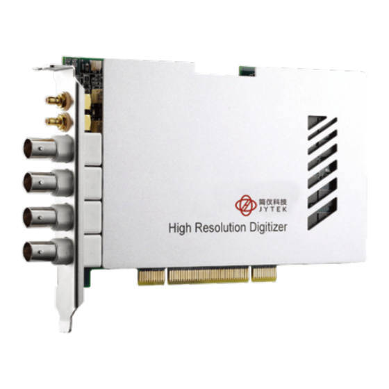
- Page 1 PCI/PXI-69816/26/46 4-CH 16-Bit 10/20/40 MS/s Digitizer with 512 MB SDRAM User’s Manual Manual Rev. : 1.00 Revision Date: Jul.16,2016...
-
Page 2: Getting Service
Getting Service Contact us should you require any service or assistance. SHANGHAI JYTEK Co., Ltd. Web site: http://www.jytek.com Address: 300 Fang Chun Rd., Zhangjiang Hi-Tech Park, Pudong New Area, Shanghai, 201203 China Tel: +86-21-5047-5899 Fax: +86-21-5047-5899 Email: service@jytek.com Additional information, aids, and tips that help users perform tasks Information to prevent minor physical injury, component damage, data loss, and/or program corruption when trying to complete a task. -
Page 3: Table Of Contents
Table of Contents Getting Service �������������������������������������������������������������������������������������������������� I 1 Introduction ������������������������������������������������������������������������������������������������ 1 1�1 Features ��������������������������������������������������������������������������������������������� 2 1.2 Applications ��������������������������������������������������������������������������������������� 2 1.3 Specifications ������������������������������������������������������������������������������������� 3 2 Getting Started �������������������������������������������������������������������������������������������14 2.1 Installation Environment �������������������������������������������������������������������14 2�2 Package Contents ������������������������������������������������������������������������������14 2�3 Mechanical Drawing and I/O Connectors �������������������������������������������15 2.4 Installing the module �������������������������������������������������������������������������17 2.5 Software Support �����������������������������������������������������������������������������18 2�5�1 WD-DASK (Legacy Drivers and Support) ����������������������������������18... - Page 4 3.7.2 SSI_TRIG1 �������������������������������������������������������������������������������34 3.7.3 SSI_TRIG2 and SSI_START_OP �������������������������������������������������35 3.7.4 Comparing the Different Trigger Sources from SSI �������������������37 3.8 Physical Location of the PXI and PCI Digitizer �������������������������������������38 3.8.1 Identify PXI Digitizer’s Physical Location by Geographic Address ���������������������������������������������������������������������������������������������������������38 3.8.2 Assign a Board ID to a PCI Digitizer �����������������������������������������38 Important Safety Instructions ��������������������������������������������������������������������������41...
- Page 5 List of Tables Table 1-1: Analog Input Specifications �������������������������������������������������������������� 3 Table 1-2: Offset and Gain Error ����������������������������������������������������������������������� 3 Table 1-3: -3dB Bandwidth, typical ������������������������������������������������������������������� 4 Table 1-4: System Noise ����������������������������������������������������������������������������������� 5 Table 1-5: Spectral Characteristics – PCI/PXI-69816 ������������������������������������������ 6 Table 1-6: Spectral Characteristics – PXI-69826 ������������������������������������������������� 7 Table 1-7: Spectral Characteristics –...
- Page 6 List of Figures Figure 1-1: PCI/PXI-69816 Bandwidth Chart (50 Ω input impedance) ���������������� 4 Figure 1-2: PCI/PXI-69826 Bandwidth Chart (50 Ω input impedance) ���������������� 5 Figure 1-3: PXI-69846 Bandwidth Chart (50 Ω input impedance) ����������������������� 5 Figure 1-4: PXI-69816 FFT with ±0.2 V Input Range�������������������������������������������� 6 Figure 1-5: PXI-69816 FFT with ±1 V Input Range ����������������������������������������������...
-
Page 7: Introduction
1 Introduction The JYTEK PCI/PXI-69816/26/46 are 10 MS/s, 20 MS/s, and 40 MS/s sampling 16-bit 4-CH digitizers designed for digitizing high frequency and wide dynamic range signals with an input frequency up to 20 MHz. The analog input range can be programmed via software to ±1 V or ±0.2 V. -
Page 8: 1�1 Features
multiple modules. Calibration The PCI/PXI-69816/26/46 include a precision on-board reference with very low temperature drift. This feature not only provides a stable calibration source for auto-calibration but also maintains stable acquisition accuracy over a wide temperature range. The automated calibration process can be done through software without need for any manually adjustments. -
Page 9: Specifications
±15V for (±1V, ±5V) ADC Resolution 16-Bit, 1 in 65536 Crosstalk ≤-80 dB at 1MHz, for all input ranges at 50 Ω input impedance Table 1-1: Analog Input Specifications Offset Error Model Name PXI-69816D PXI-69846H, PXI-69826D PCI-69816H PXI-69846D PCI-69826H PXI-69846W PCI-69846H... -
Page 10: Table 1-3: -3Db Bandwidth, Typical
-3dB Bandwidth, typical Input Range PXI-69816D PXI -69826D PXI-69846D PXI-69846W PCI-69846D @50 Ω and 1 MΩ impedance ±0.2 V, ±1 V 5.1 MHz 9.6 MHz 20 MHz 80 MHz (±1 V) 50 MHz (±0.2 V) Input Range PCI-69816H PCI-69826H PXI-69846H PCI-69846H @50 Ω... -
Page 11: Table 1-4: System Noise
Figure 1-2: PCI/PXI-69826 Bandwidth Chart (50 Ω input impedance) Figure 1-3: PXI-69846 Bandwidth Chart (50 Ω input impedance) System Noise (measured and calculated under 50 Ω input impedance) Input Range PXI-69816D PXI-69826D PXI-69846D PXI-69846W PCI-69846D ±0.2 V 5.0 LSB 6.0 LSB 8.0 LSB... -
Page 12: Table 1-5: Spectral Characteristics - Pci/Pxi-69816
Spectral Characteristics – PXI-69816 Specification Input Range ±1 V ±0�2 V Signal to Noise and Distortion (SINAD), typical 79.11 dBc 75.93 dBc Signal-to-Noise Ratio (SNR), typical 79.36 dBc 75.96 dBc Total Harmonic Distortion (THD), typical -89.90 dBc -95.77 dBc Spurious Free Dynamic Range (SFDR), typical 90.37 dBc 98.65 dBc Effective Number of Bit (ENOB), typical... -
Page 13: Table 1-6: Spectral Characteristics - Pxi-69826
Figure 1-5: PXI-69816 FFT with ±1 V Input Range Spectral Characteristics – PXI-69826 Specification Input Range ±1 V ±0�2 V Signal to Noise and Distortion (SINAD), typical 78.63 dBc 74.44 dBc Signal-to-Noise Ratio (SNR), typical 79.95 dBc 74.48 dBc Total Harmonic Distortion (THD), typical -88.29 dBc -93.52 dBc Spurious Free Dynamic Range (SFDR), typical... -
Page 14: Figure 1-6: Pxi-69826 Fft With ±0.2 V Input Range
Figure 1-6: PXI-69826 FFT with ±0.2 V Input Range PXI-69826 +/-1V, S-Rate = 20MS/s, Input Signal = 0.998 MHz @ -1.0796 dBF PXI-9826 +/ -1V, S-Rate = 20MS/s, I nput Signal = 0.998 MHz @ -1.0796 dBF -100 -120 Frequency (Hz) x 10 Figure 1-7: PXI-69826 FFT with ±1 V Input Range... -
Page 15: Table 1-7: Spectral Characteristics - Pci/Pxi-69846
Spectral Characteristics – PXI-69846 Specification Input Range ±1 V ±0�2 V Signal to Noise and Distortion (SINAD), typical 76.06 dBc 71.97 dBc Signal-to-Noise Ratio (SNR), typical 76.17 dBc 71.98 dBc Total Harmonic Distortion (THD), typical -90.65 dBc -95.78 dBc Spurious Free Dynamic Range (SFDR), typical 91.62 dBc 96.15 dBc Effective Number of Bit (ENOB), typical... -
Page 16: Figure 1-9: Pxi-69846 Fft With ±1 V Input Range
PXI-69846, +/-1V, S-Rate = 40MS/s, Input Signal = 0.998 MHz @ -1.1732 dBFs PXI-9846, +/-1V, S-Rate = 40MS/s, I nput Signal = 0.998 MHz @ -1.1732 dBFs -100 -120 Frequency (Hz) x 10 Figure 1-9: PXI-69846 FFT with ±1 V Input Range... - Page 17 Timebase Specification Value Sample Clock Internal: onboard oscillator External: CLK IN (front panel SMB connector), PXI STAR, Sources PXI Trigger Bus[0..7], PXI 10MHz, SSI bus PCI/PXI-69816 PCI/PXI-69826 PCI/PXI-69846 Timebase Frequency 10 MHz-1 MHz 20 MHz-1 MHz 40 MHz-1 MHz Range Sampling Rate Range 10 MS/s-0.596 S/s 20 MS/s-1.192 S/s...
-
Page 18: Table 1-9: Triggering
Triggering Specification Value Trigger Sources Software, TRG IO (front panel SMB connector), analog trigger from CH0~CH3, PXI STAR, PXI Trigger Bus[0..7], SSI bus Trigger Modes Pre-trigger, Post-trigger, Middle-trigger, Delaytrigger TRG IO, as input port Connector type Compatibility 3.3 V LVTTL, 5 V tolerant Input Level High threshold (V ): 2.0 V, minimum... -
Page 19: Table 1-12: General Information
General Information Specification Value Environment Operating Environment Ambient temperature: 0°C to +55°C for PXI version, 0°C to +50°C for PCI version Relative humidity: 10% to 90%, non-condensing Storage Environment Ambient temperature: -20°C to +85°C Relative humidity: 10% to 90%, non-condensing Physical PCB Dimension PXI version: Single 3U PXI module, 100 mm by 160 mm... -
Page 20: Getting Started
Do not install or apply power to equipment that is damaged or if there is missing/ incomplete equipment. Retain the shipping carton and packing materials for inspection. Please contact your JYTEK immediately for assistance. Obtain authorization before returning any product to JYTEK. ... -
Page 21: 2�3 Mechanical Drawing And I/O Connectors
Figure 2-1: PXI-698x6 Mechanical Drawing Figure 2-2: PCI-698x6 Mechanical Drawing The JYTEK PXI-69816/PXI-69826/PXI-69846 is packaged in a Eurocard form factor with PXI specifications measuring 160 mm in length and 100 mm in height (not including connectors). The PCI69816/69826/69846 is a half-length and standard height PCI form factor. Please... -
Page 22: Table 2-1: Connector Pin Assignments
The connector types and functions are described as follows. Connector Direction Type Description/Function CLK IN Input The CLK IN is a 50Ω, AC-coupled external timebase input. TRG IO Input Output The TRG IO is a bidirectional port for external digital trigger input or output. -
Page 23: Installing The Module
2.4 Installing the module To install the PXI-69816/PXI-69826/PXI-69846 module: 1. Turn off the PXI system/chassis and disconnect the power plug from the power source. 2. Align the module’s edge with the card guide in the PXI chassis. 3. Slide the module into the chassis, until resistance is felt from the PXI connector. 4. -
Page 24: Software Support
2�5 Software Support JYTEK provides comprehensive software drivers and packages to suit various user approaches to building a system. Aside from programming libraries, such as DLLs, for most Windows-based systems, JYTEK also provides drivers for other application environment. 2�5�1 WD-DASK (Legacy Drivers and Support) WD-DASK is composed for advanced 32-bit kernel drivers for customized DAQ application development. -
Page 25: Operation Theory
3 Operation Theory The operation theory of the PCI/PXI-69816/26/46 is described in this chapter, including the control and setting of signal sources, trigger sources, trigger modes, data transfers, and synchronizing multiple modules. 3.1 Functional Block Diagram Figure 3-1: PCI-698x6 Functional Block Diagram Figure 3-2: PCI-698x6 Functional Block Diagram... -
Page 26: Basic Ai Acquisition
3.2 Basic AI Acquisition In this section, we are going to explain the basic acquisition timing. 3�2�1 Analog Input Path The following figure shows the block diagram of the single analog input path of a digitizer. Each path provides a choice of 50 Ω input impedance or high impedance. The gain amplifier is optimized for each input range with low noise and high dynamic range. -
Page 27: Table 3-1: Basic Counters
Counter Name Length Valid value Description Scan Intrv 24-bit 1 - 16777215 Scan Interval Counter This counter is a TIMEBASE divider to the achieve equivalent sampling rate of digitizer. The equation is: Sampling rate = TIMEBASE / Scan Intrv The value of TIMEBASE depends on the card type. -
Page 28: Ai Data Format
Analog signal TIMEBASE Trigger Acquisition Acquisition starts right after this clock edge In Progress D254 D256 DATA D253 Trigger mode = post-trigger, DataCnt = 256, ScanIntrv = 1 Figure 3-4: Basic Acquisition Timing Of Digitizer 3.2.3 AI Data Format The following table illustrates the idea transfer characteristics of various input ranges of the PCI/PXI-69816/26/46. -
Page 29: Adc Sampling Rate And Timebase Control
3.3 ADC Sampling Rate and TIMEBASE Control The PXI/PCI-698X6 supports several timebase sources for analog input conversion: • Internal oscillator • External clock through front panel • PXI_STAR (PCI version) • PXI Trigger Bus[0..7] (PXI version) • PXI 10M (PXI version) •... -
Page 30: External Clock From Pxi Interfaces
3.3.3 External Clock from PXI Interfaces The PCI/PXI-69816/26/46 can receive timebase via one of the PXI Trigger Bus lines by software selection. The eight PXI Trigger Bus lines (PXI_TRIG[0..7]) provide inter-module synchronization and communication. Note that this function is only available when the PCI/ PXI-69816/26/46 is in a PXI system. -
Page 31: 3�4 Trigger Sources
3�4 Trigger Sources In addition to the internal software trigger, the PCI/PXI-69816/26/46 also supports external analog triggers, external digital triggers, PXI_STAR triggers, PXI Trigger Bus[0..7] and SSI bus.. You can configure the trigger source by software command. Please refer to Figure 3.7 for trigger architecture. -
Page 32: 3�4�3 Analog Trigger
3�4�3 Analog Trigger You can choose either CH0, CH1, CH2 or CH3 as the trigger signal while using external analog trigger source. The trigger level can be set by software with 8-bit resolution. Please refer to Table 3-3 for the ideal transfer characteristic. Trigger Level Setting (Hex) Trigger Voltage (-1V to +1V Trigger Voltage (-0�2V to... -
Page 33: Pxi Star Trigger
3.4.4 PXI STAR Trigger When you select PXI STAR as the trigger source, the PXI-69816/ PXI-69826/PXI-69846 can accept a TTL-compatible digital signal as a trigger signal. The trigger occurs when a rising edge or falling edge is detected at PXI STAR. You can use software to configure the trigger polarity. -
Page 34: 3�5 Trigger Modes
3�5 Trigger Modes There four trigger modes working with trigger sources to initiate different data acquisition timing when a trigger event occurs. They are described in this section. 3.5.1 Post-trigger Acquisition Use post-trigger acquisition when you want to collect data after the trigger event, as illustrated in Figure 3-11. -
Page 35: Middle-Trigger Acquisition
The trigger event occurs after the specified amount of data has been acquired. However, if the trigger event occurs before the specified amount of data has been acquired, the acquisition engine will ignore the trigger signal until the specified amount of data has been acquired. -
Page 36: Post-Trigger Or Delay-Trigger Acquisition With Retrigger
maximum delay time is the period of TIMEBASE X (2 - 1), while the minimum delay is the period of timebase. Acquisition stop Trigger Event Begin to transfer data to Operation Acquisition start Occurs system start Delay Time Time Trigger Data N samples Figure 3-15: Delay-trigger Mode Operation... -
Page 37: 3�6 Data Transfers
3�6 Data Transfers Since the maximum data throughput on the PCI/PXI-69846 (40MS/ s * 4 channels *2 Bytes/ channel = 320MB/s) is much higher than the 32bit/33MHz PCI-bus bandwidth, samples are acquired into the onboard SDRAM memory before being transferred to the host computer. Since the number of stored samples per acquisition is limited by the amount of on-board memory, the PCI/PXI-69816/26/ 46 supports maximum 512MB in order to meet application requirements. -
Page 38: Synchronizing Multiple Modules
3�7 Synchronizing Multiple Modules The eight interconnected lines on PXI backplane named as PXI Trigger Bus[0:7] provide a flexible interface for multiple modules synchronization. The PXI-69816/26/46 utilizes the PXI Trigger Bus[0:7] as the System Synchronization Interface (SSI). By providing flexible routing of timebase clock and trigger signals onto PXI Trigger Bus, the PXI-69816/26/46 makes the synchronization between multiple modules easy and simple. -
Page 39: Figure 3-19: Ssi Connector Location On The Pci-69816/26/46
For PCI-69816/26/46, a dedicate connector is served as system synchronization interface. Refer to Figure 3-19 for the connector position. All the SSI signals are routed to the 20-pin connector from FPGA. With this interface, PCI-69816/26/46 is capable of achieving multiple module synchronization. -
Page 40: Ssi_Timebase
19 17 15 13 11 CN11 20 18 16 14 12 10 8 Signal Name Direction Description Location SSI_TIMEBASE Input/Output Timebase signal pin 1 through SSI SSI_TRIG1 Input/Output Trigger signal through pin 11 SSI_TRIG2 Input/Output Clocked trigger signal pin 9 through SSI SSI_START_OP Input/Output... -
Page 41: Ssi_Trig2 And Ssi_Start_Op
SSI_TRIG1 (Output) Two = 3-4 TIMEBASE Clocks SSI_TRIG1 (Input) Twi = 20 ns minimum Figure 3-21: SSI_TRIG1 Input and Output Timing Characteristics 3.7.3 SSI_TRIG2 and SSI_START_OP As an output, the SSI_TRIG2 signal is a clocked SSI_TRIG1 signal by TIMEBASE, as illustrated in Figure 3-22. -
Page 42: Figure 3-23: Ssi_Trig2 Input Timing Requirement
SSI_TRIG2 Tw = 20 ns minimum Figure 3-23: SSI_TRIG2 Input Timing Requirement As an output, the SSI_START_OP signal reflects the operation start signal in a pre-trigger or middle-trigger acquisition sequence. Please refer to Figure 3-12 - Figure 3-14 for the relationship between the operation start signal and the acquisition sequence. -
Page 43: Comparing The Different Trigger Sources From Ssi
3.7.4 Comparing the Different Trigger Sources from SSI When selecting TRSRC_SSI_1 as the trigger source input, the signal SSI_TRIG1 reflects the trigger event signal in an acquisition sequence. However, when synchronizing multiple PCI/ PXI-69816/ 26/46 devices, each module may recognize the trigger signal with one-clock time difference because the signal is not related to the timebase. -
Page 44: Physical Location Of The Pxi And Pci Digitizer
3�8 Physical Location of the PXI and PCI Digitizer 3�8�1 Identify PXI Digitizer’s Physical Location by Geographic Address Compact PCI and PXI chassis accommodate slot numbering mechanism based on the definition of Geographical Address pins on its backplane. Users can identify module’s physical location by reading back Geographical Address. -
Page 45: Figure 3-26: Enlargement Of Board Id Setting
Figure 3-26: Enlargement of Board ID setting. Only dip switches 1-5 are valid for board ID settings. Dip switches 6- 9 are unused. When a dip switch is switched to ‘ON’, it represents ‘1’, the opposite direction represents ‘0’. -
Page 46: Table 3-6: Board Id Combination Conditions
Board ID Switch Number 1: ON 0: OFF Table 3-6: Board ID Combination Conditions... -
Page 47: Important Safety Instructions
Important Safety Instructions Please read and follow all instructions marked on the product and in the documentation before operating the system. Retain all safety and operating instructions for future use. • Please read these safety instructions carefully. • Please keep this User’s Manual for future reference. •... - Page 48 ◦ Liquid has penetrated the equipment. ◦ The equipment has been exposed to moisture. ◦ The equipment is not functioning or does not function according to the user’s manual. ◦ The equipment has been dropped and damaged. ◦ If the equipment has obvious sign of breakage. •...
Need help?
Do you have a question about the PXI-69816D and is the answer not in the manual?
Questions and answers