Sign In
Upload
Manuals
Brands
JYTEK Manuals
Measuring Instruments
PXIe-69834
User Manuals: JYTEK PXIe-69834 PXIe Digitizer
Manuals and User Guides for JYTEK PXIe-69834 PXIe Digitizer. We have
1
JYTEK PXIe-69834 PXIe Digitizer manual available for free PDF download: User Manual
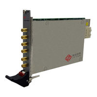
JYTEK PXIe-69834 User Manual (64 pages)
4CH 16-bit 80MS/s PXIe Digitizer
Brand:
JYTEK
| Category:
Measuring Instruments
| Size: 5 MB
Table of Contents
Table of Contents
7
List of Figures
9
List of Tables
11
Introduction
13
Features
13
Applications
14
Specifications
14
Analog Input
14
Table 1-1: Analog Input Channel Characteristics
14
Accuracy
15
System Noise
15
Crosstalk, DC to 10Mhz
15
Table 1-2: Accuracy
15
Table 1-3: System Noise
15
Table 1-4: Crosstalk, DC to 10Mhz
15
Spectral Characteristics
16
Figure 1-1: Typical Frequency Response, 1MΩ Input Impedance
16
Table 1-5: Spectral Characteristics
16
Figure 1-2: Typical Frequency Response, 50Ω Input Impedance
17
Timebase
18
Table 1-6: Timebase Specifications
18
Triggers
19
Table 1-8: External Reference Clock
19
Table 1-9: Triggers
19
Table 1-10: External Digital Trigger Input
20
Table 1-11: Onboard Reference (Calibration)
20
Mechanical and Environmental
21
Power Consumption
21
Table 1-12: Specifications
21
Table 1-13: Power Consumption
21
Software Support
22
Figure 1-3: JYTEK MAPS Architecture
22
MAPS Core
23
Figure 1-4: JYTEK Connection Explorer (ACE)
24
Figure 1-5: JYTEK Connection Explorer Soft Front Panel
25
MAPS/C, C & C++ Support
26
Device Layout and I/O Connectors
27
Figure 1-6: Pxie-69834 Dimensions
27
Figure 1-7: Pxie-69834 Front Panel
28
Table 1-14: Pxie-69834 I/O Array Legend
29
Getting Started
31
Installation Environment
31
Package Contents
32
Installing the Module
33
Operations
35
Functional Block Diagram
35
Analog Input Channel
35
Analog Input Front-End Configuration
35
Figure 3-1: Functional Block Diagram
35
Figure 3-2: Analog Input Architecture
35
Input Range and Data Format
36
Table 3-1: Input Range and Data Format
36
Table 3-2: Input Range FSR and -FSR Values
37
Table 3-3: Input Range Midscale Values
37
DMA Data Transfer
38
Trigger Source
39
Figure 3-3: Linked List of PCI Address DMA Descriptors
39
Figure 3-4: Trigger Architecture
39
Software Trigger
40
External Digital Trigger
40
Figure 3-5: External Digital Trigger
40
Analog Trigger
41
Figure 3-6: Analog Trigger Conditions
41
PXI Trigger Bus
42
PXI Star
42
Pxie Differential Trigger
42
Trigger Modes
43
Post Trigger Mode
43
Figure 3-7: Post-Trigger Acquisition
43
Delayed Trigger Mode
44
Pre-Trigger Mode
44
Figure 3-8: Delayed Trigger Mode Acquisition
44
Figure 3-9: Pre-Trigger Mode Acquisition
44
Middle Trigger Mode
45
Figure 3-10: Middle Trigger Mode Acquisition
45
Acquisition with Re-Triggering
46
Figure 3-11: Re-Trigger Mode Acquisition
46
Timebase
47
Internal Sampling Clock
47
Figure 3-12: Timebase Architecture
47
External Reference Clock
48
Acquisition Timing Control
49
Figure 3-13: Varying Sampling Rates Via Scan Interval Counter
49
Table 3-4: Counter Parameters and Description
50
Synchronizing Multiple Modules
51
Figure 3-14: Non-Synched Digitizer Modules
51
Figure 3-15: External Instrument Synchronization
52
Figure 3-16: Module-Based Synchronization
53
Figure 3-17: Pxie Instrumentation Signals
54
Multi-Module Synchronization Interfaces
55
Figure 3-18: Trigger Architecture
55
Figure 3-19: PXI_CLK10 as 10Mhz Reference
56
A Appendix: Calibration
57
Calibration Constant
57
Auto-Calibration
58
Figure A-1: Auto-Calibration Block Diagram
58
Figure A-2: Auto-Calibration Flow
59
Important Safety Instructions
61
Advertisement
Advertisement
Related Products
JYTEK PXIe-69852
JYTEK PXI-69816D
JYTEK PXI-69826D
JYTEK PXI-69846D
JYTEK PXI-69846W
JYTEK PXI-69846H
JYTEK PCIe-69814 Series
JYTEK PCIe-69814P
JYTEK PCI-69846D
JYTEK PCI-69846H
JYTEK Categories
Computer Hardware
Control Unit
Controller
Measuring Instruments
Chassis
More JYTEK Manuals
Login
Sign In
OR
Sign in with Facebook
Sign in with Google
Upload manual
Upload from disk
Upload from URL