Table of Contents
Advertisement
Quick Links
SERVICE MANUAL
Ver. 1.1 2006.10
• HCD-CPZ1DAB is the amplifier, CD player, tape
deck and tuner section in CMT-CPZ1DAB.
US and foreign patents licensed from Dolby
Laboratories.
Main unit
Amplier section
DIN power ou tput (ra ted): 60 + 60 W (4 ohms at 1 kHz, DIN)
Continuous RMS power output (reference): 75 + 75 W (4 ohms at 1 kHz, 10%
THD)
Outputs
CD DIGITAL OUT: Optical Wavelength: 660 nm
PHONES (stereo mini jack): Accepts headphones with an impedance of 8
ohms or more
SPEAKER: Accepts impedance of 4 ohms
CD player section
System: Compact disc and digital audio system
Laser Diode Properties
Emission Duration: Continuous
Laser Output*: Less than 44.6µW
* This output is the value measurement at a distance of 200 mm from the
objective lens surface on the Optical Pick-up Block with 7 mm aperture.
Frequency response: 20 Hz – 20 kHz (±1 dB)
Wavelength: 770 – 810 nm
Tape deck section
Recording system: 4-track 2-channel, stereo
Tuner section
DAB tuner section:
Frequency range
Band-III: 174.928 (5A) – 239.200 (13F) MHz
* For details, see "DAB frequency table" below.
Antenna: FM/DAB lead antenna
Antenna terminal: 75 ohms, F female
Sony Corporation
9-887-335-02
Personal Audio Division
2006J05-1
Published by Sony Techno Create Corporation
© 2006.10
HCD-CPZ1DAB
Model Name Using Similar Mechanism
CD
CD Mechanism Type
Section
Base Unit Name
Optical Pick-up Block Name
TAPE
Model Name Using Similar Mechanism
Section
Tape Transport Mechanism Type
SPECIFICATIONS
FM stereo, FM/AM superheterodyne tuner
FM tuner section:
Tuning range: 87.5 – 108.0 MHz (50 kHz step)
Antenna: FM lead antenna
Antenna terminals: 75 ohms unbalanced
Intermediate frequency: 10.7 MHz
AM tuner section:
Tuning range: 531 − 1,602 kHz (with the tuning interval set at 9 kHz)
Antenna: AM loop antenna
Antenna terminals: External antenna terminal
Intermediate frequency: 450 kHz
DAB frequency table (Band-III)
Frequency
Label
Frequency
174.928 MHz
5A
209.936 MHz
176.640 MHz
5B
211.648 MHz
178.352 MHz
5C
213.360 MHz
180.064 MHz
5D
215.072 MHz
181.936 MHz
6A
216.928 MHz
183.648 MHz
6B
218.640 MHz
185.360 MHz
6C
220.352 MHz
187.072 MHz
6D
222.064 MHz
188.928 MHz
7A
223.936 MHz
COMPACT DISC DECK RECEIVER
NEW
CDM80BH-K6BD83S-WD
BU-K6BD83S-WD
KSM-213DCP
HCD-CPZ1
CMAL1Z255A
Frequency
Label
190.640 MHz
7B
192.352 MHz
7C
194.064 MHz
7D
195.936 MHz
8A
197.648 MHz
8B
199.360 MHz
8C
201.072 MHz
8D
202.928 MHz
9A
204.640 MHz
9B
Label
206.352 MHz
9C
10A
208.064 MHz
9D
10B
General
10C
Power requirements: 230 V AC, 50/60 Hz
10D
Power consumption: 60 watts
Dimensions (w/h/d) (excl. speakers): Approx. 175 × 240 × 300 mm
11A
Mass (excl. speakers): Approx. 3.9 kg
11B
Design and specications are subject to change without notice.
11C
11D
12A
UK Model
Frequency
Label
225.648 MHz
12B
227.360 MHz
12C
229.072 MHz
12D
230.784 MHz
13A
232.496 MHz
13B
234.208 MHz
13C
235.776 MHz
13D
237.488 MHz
13E
239.200 MHz
13F
Advertisement
Table of Contents

Related Manuals for Sony HCD-CPZ1DAB


Summary of Contents for Sony HCD-CPZ1DAB
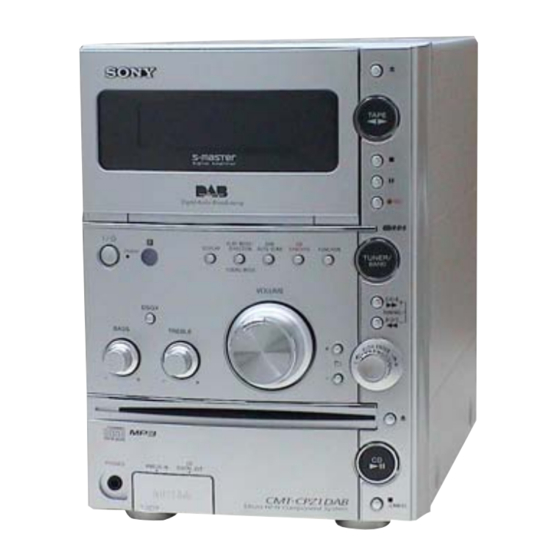
- Page 1 HCD-CPZ1DAB SERVICE MANUAL UK Model Ver. 1.1 2006.10 • HCD-CPZ1DAB is the amplifier, CD player, tape deck and tuner section in CMT-CPZ1DAB. US and foreign patents licensed from Dolby Model Name Using Similar Mechanism Laboratories. CD Mechanism Type CDM80BH-K6BD83S-WD Section...
-
Page 2: Table Of Contents
COMPONENTS IDENTIFIED BY MARK 0 OR DOTTED LINE WITH MARK 0 ON THE SCHEMATIC DIAGRAMS AND IN THE PARTS LIST ARE CRITICAL TO SAFE OPERATION. REPLACE THESE COMPONENTS WITH SONY PARTS WHOSE PART NUMBERS APPEAR AS SHOWN IN THIS MANUAL OR IN SUPPLEMENTS PUBLISHED BY SONY. -
Page 3: Servicing Notes
HCD-CPZ1DAB SECTION 1 SERVICING NOTES NOTES ON HANDLING THE OPTICAL PICK-UP BLOCK OR BASE UNIT The laser diode in the optical pick-up block may suffer electrostatic break-down because of the potential difference generated by the charged electrostatic load, etc. on clothing and the human body. -
Page 4: General
HCD-CPZ1DAB SECTION 2 This section is extracted from instruction manual. GENERAL Basic Operations Notes Notes on loading discs Press • If your country or region does not support DAB broadcast, “No • When you turn on the system, the disc is not pulled into the disc slot... - Page 5 HCD-CPZ1DAB Other Operations Play Timer: Creating your own CD program Recording onto a tape You can wake up to CD, tape or tuner at a preset time. Rec Timer: (Program Play) You can record on a TYPE I (normal) tape in two ways: You can record a preset radio station at a specied time.
-
Page 6: Disassembly
HCD-CPZ1DAB SECTION 3 DISASSEMBLY • This set can be disassembled in the order shown below. 3-1. DISASSEMBLY FLOW 3-2. CASE (Page 7) 3-3. FRONT PANEL SECTION (Page 7) 3-4. TC BOARD, 3-6. MAIN BOARD MECHANICAL DECK (Page 9) (CMAL1Z255A) (Page 8) 3-7. -
Page 7: Case
HCD-CPZ1DAB Note: Follow the disassembly procedure in the numerical order given. 3-2. CASE 4 case 2 three screws (B3) 1 two screws (case 3 TP2) 1 two screws (case 3 TP2) 3-3. FRONT PANEL SECTION 8 two connectors 1 wire (flat type) (19 core) -
Page 8: Tc Board, Mechanical Deck (Cmal1Z255A)
HCD-CPZ1DAB 3-4. TC BOARD, MECHANICAL DECK (CMAL1Z255A) 6 terminal 5 four screws (BVTP3 × 8) 1 flexible flat cable (8 core) 4 TC board 7 mechanical deck 3 connector (CMAL1Z255A) 2 three screws (PTPWH 2) 3-5. PANEL BOARD q; lid (TC) section... -
Page 9: Main Board
HCD-CPZ1DAB 3-6. MAIN BOARD 2 back panel 1 six screws (B3) 5 two connectors (CN201, CN202) 1 three screws (B3) 3 flexible flat cable (21 core) (CN302) qa MAIN board 4 flexible flat cable (9 core) 8 connector (CN310) (CN306) -
Page 10: Dab Module Assy
HCD-CPZ1DAB 3-8. DAB MODULE ASSY 1 nut 4 harness 3 connector 5 Remove a solder. 8 DAB module assy 7 DAB board 6 connector 2 two screws (BVTP3 × 6) 3-9. CHASSIS (TOP) 1 screw (BVTP2.6) 3 three screws (BVTP2.6) -
Page 11: Lever (Loading-L/R)
HCD-CPZ1DAB 3-10. LEVER (LOADING-L/R) SPR-T (loading-R) SPR-T (loading-L) 6 lever (loading-R) 3 two hooks 5 two hooks 4 lever (loading-L) PRECAUTION DURING LEVER (LOADING-R / L) INSTALLATION Align the horizontal position. lever (loading-L) lever (loading-R) Install the both levers so that they move symmetrically. -
Page 12: Lever (Disc Sensor), Lever (Disc Stop)
HCD-CPZ1DAB 3-11. LEVER (DISC SENSOR), LEVER (DISC STOP) 1 gear (cap) 2 gear (IDL-L) PRECAUTION DURING LEVER (DISC STOP) INSTALLATION chassis (top) hole 5 two hooks 3 two claws lever (disc stop) 6 lever (disc stop) hole Install the lever (disc stop) so that the both holes are aligned. -
Page 13: Cd Board
HCD-CPZ1DAB 3-13. CD BOARD 1 Remove soldering 5 CD board from the four points. 3 sheet 4 flexible flat cable (23 core) (CN102) 2 wire (flat type) (16 core) (CN301) 3-14. BU SECTION 4 floating screw 6 BU section (PTPWH M2.6) -
Page 14: Optical Pick-Up Block (Ksm-213Dcp)
HCD-CPZ1DAB 3-15. OPTICAL PICK-UP BLOCK (KSM-213DCP) 1 two screws (BTTP M2.6) 6 two insulators 7 optical pick-up block 2 two stoppers (BU) 4 two floating screws (KSM-213DCP) (PTPWH M2.6) 3 two coil springs (insulator) 5 two coil springs (insulator) 6 two insulators 3-16. -
Page 15: Close Lever
HCD-CPZ1DAB 3-17. CLOSE LEVER 1 washer (3-1-0.4) 5 close lever 3 claw 2 SPR-E lever close 4 shaft disc stop 3-18. LEVER (DIR), GEAR (IDL-B) 2 capstan retaining ring 3 pulley (gear) 4 gear (cap) 5 gear (IDL-A) 8 stopper 9 lever (DIR) q;... -
Page 16: Gear (Idl-C)
HCD-CPZ1DAB 3-19. GEAR (IDL-C) 3 gear (IDL-D) 2 two claws 4 three hooks 1 gear (IDL-F) 5 lever (gear loading) 7 gear (IDL-C) 6 claw... -
Page 17: Test Mode
HCD-CPZ1DAB SECTION 4 TEST MODE COMMON TEST MODE SHIP MODE (NO MEMORY CLEAR) • This mode is used to check operations of Amplifier. • This mode moves the optical pick-up to the position durable Procedure: to vibration. Use this mode when returning the set to the 1. - Page 18 HCD-CPZ1DAB CD SERVO TEST MODE • This mode used to ckeck operation of optical pick-up. Procedure: 1. Press the I/1 key to turn the power ON. 2. Press the [FUNCTION] key to select “CD”. 3. Press three keys of [PLAY MODE/DIRECTION/TUNING MODE], l m and x (CD) simultaneously.
-
Page 19: Mechanical Adjustments
HCD-CPZ1DAB SECTION 5 SECTION 6 MECHANICAL ADJUSTMENTS ELECTRICAL ADJUSTMENTS PRECAUTION 3. Mode: Playback DECK SECTION 0 dB=0.775 V CD SECTION 1. Clean the following parts with a denatured alcohol-moistened test tape swab: HP/MD board 1. Demagnetize the record/playback head with a head... -
Page 20: Diagrams
HCD-CPZ1DAB SECTION 7 DIAGRAMS 7-1. BLOCK DIAGRAM – CD SERVO/TAPE DECK Section – DETECTOR +3.3V CD-L 58 B AOUT1 (Page 21) RFACO 71 RFACI PCMD 4 PCMDI 59 C AOUT2 R-CH 6 BCKI 60 D LRCK 2 LRCKI 50 E... -
Page 21: Block Diagram - Main Section
HCD-CPZ1DAB 7-2. BLOCK DIAGRAM – MAIN Section – TAPE REC-L (Page 20) J982 HEADPHONE R-CH PHONES IC502 MUTING J981 Q414 ANALOG R-CH INPUT SELECT, ELECTRICAL VOLUME R-CH IC501 MUTING CONTROL A/D CONVERTER STREAM PROCESSOR POWER DRIVER SEL1 2 Q403, 404... -
Page 22: Block Diagram - Panel/Key/Power Supply Section
HCD-CPZ1DAB 7-3. BLOCK DIAGRAM – PANEL/KEY/POWER SUPPLY Section – D901 LED DRIVE LED STAND BY Q901 STANDBY 35 LCD DATA LIQUID D902 36 LCD-CLK CRYSTAL LED DRIVE LED TUNER 66 78 LCD CS TUNER/ DISPLAY Q902 BAND LCD951 63 LCD RESB... - Page 23 HCD-CPZ1DAB • Note for Printed Wiring Boards and Schematic Diagrams • Circuit Boards Location Note on Printed Wiring Board: Note on Schematic Diagram: • X : parts extracted from the component side. • All capacitors are in µF unless otherwise noted. (p: pF) •...
-
Page 24: Printed Wiring Board - Cd Board
HCD-CPZ1DAB • See page 23 for Circuit Boards Location. 7-4. PRINTED WIRING BOARD – CD Board – :Uses unleaded solder. CD BOARD (COMPONENT SIDE) CD BOARD M401 (SPINDLE) (CONDUCTOR SIDE) S201 (LIMIT) R280 C405 C406 R451 IC402 R104 R105 C104... -
Page 25: Schematic Diagram - Cd Board
HCD-CPZ1DAB • See page 48 for Waveforms. • See page 48 for IC Block Diagrams. • See page 53 for IC Pin Function Description. 7-5. SCHEMATIC DIAGRAM – CD Board – C210 C208 (RFACI) C230 R256 100p C257 C274 CN301... -
Page 26: Printed Wiring Board - Tc Board
HCD-CPZ1DAB • See page 23 for Circuit Boards Location. 7-6. PRINTED WIRING BOARD – TC Board – :Uses unleaded solder. • Semiconductor Location Ref. No. Location D641 TC BOARD D681 HRPE601 (REC/PLAY/ERASE) IC601 L-CH Q601 Q602 R-CH Q638 Q640 Q642... -
Page 27: Schematic Diagram - Tc Board
HCD-CPZ1DAB Ver. 1.1 • See page 48 for Waveforms. 7-7. SCHEMATIC DIAGRAM – TC Board – FFC601 Q601,602,651,652 Q680,681,688 PLAY SW REC/PB SWITCH Q681 REC/PB SWITCH R662 RT1P141C R REC Q692,694 Q691,693 F REC FFC601 CAPSTAN/REEL TRIGGER Q651 Q601 PACK... -
Page 28: Printed Wiring Board - Dab Board
HCD-CPZ1DAB Ver. 1.1 • See page 23 for Circuit Boards Location. 7-8. PRINTED WIRING BOARD – DAB Board – :Uses unleaded solder. ANTENNA DAB MODULE DAB 75Ω DAB BOARD C832 R838 R831 FFC310 MAIN BOARD CN310 EP801 (Page 31) 12, 13... -
Page 29: Schematic Diagram - Dab Board
HCD-CPZ1DAB • See page 48 for IC Block Diagrams. 7-9. SCHEMATIC DIAGRAM – DAB Board – ANTENNA DAB 75Ω R803 C811 470p R805 R807 4.7k DAB MODULE R809 R827 R825 4.7k 100k 4.7k C813 CN800 100p R823 C817 R813 100k... -
Page 30: Printed Wiring Board - Driver Board
HCD-CPZ1DAB • See page 23 for Circuit Boards Location. • See page 48 for IC Block Diagrams. 7-10. PRINTED WIRING BOARD – DRIVER Board – 7-11. SCHEMATIC DIAGRAM – DRIVER Board – :Uses unleaded solder. IC701 BA6956AN (CHUCK) S701 S702... -
Page 31: Printed Wiring Board - Main Board
HCD-CPZ1DAB • See page 23 for Circuit Boards Location. 7-12. PRINTED WIRING BOARD – MAIN Board – :Uses unleaded solder. • Semiconductor Location (Page 36) (Page 28) (Page 26) Ref. No. Location TC BOARD AMP BOARD DAB BOARD CN603 CN700... -
Page 32: Schematic Diagram - Main Board (1/2)
HCD-CPZ1DAB • See page 48 for IC Block Diagrams. 7-13. SCHEMATIC DIAGRAM – MAIN Board (1/2) – CN301 M+12V (1/2) MGND INPUT SELECT,ELECTRICAL VOLUME TRIG SOL IC501 C503 BD3872FS CAP MOT C527 R523 +3.3V +7V REGULATOR R522 END-SW FILTER IC201 TA7807S HALF.REC... -
Page 33: Schematic Diagram - Main Board (2/2)
HCD-CPZ1DAB • See page 48 for Waveforms. • See page 48 for IC Block Diagrams. • See page 53 for IC Pin Function Description. 7-14. SCHEMATIC DIAGRAM – MAIN Board (2/2) – (2/2) D302 MC2836 (Page 32) CN309 RDS DATA... -
Page 34: Schematic Diagram - Amp Board (1/2)
HCD-CPZ1DAB • See page 48 for Waveforms. • See page 48 for IC Block Diagrams. 7-15. SCHEMATIC DIAGRAM – AMP Board (1/2) – (1/2) R783 CN700 C731 OSC BUFFER L701 D701 1SS355W IC709 TC7SHU04FU A+5V AGND C786 R IN C748 0.001... -
Page 35: Schematic Diagram - Amp Board (2/2)
HCD-CPZ1DAB • See page 48 for IC Block Diagrams. 7-16. SCHEMATIC DIAGRAM – AMP Board (2/2) – (2/2) EP705 (CHASSIS) EP706 (CHASSIS) EP702 POWER DRIVER (CHASSIS) EP701 IC707 CXD9774M C842 C843 C840 C841 C828 C839 C829 1000p 1000p (CHASSIS) R704... -
Page 36: Printed Wiring Board - Amp Board
HCD-CPZ1DAB • See page 23 for Circuit Boards Location. 7-17. PRINTED WIRING BOARD – AMP Board – :Uses unleaded solder. • Semiconductor Location Ref. No. Location AMP BOARD AMP BOARD (COMPONENT SIDE) (CONDUCTOR SIDE) D701 (CHASSIS) D702 D703 D704 D705... -
Page 37: Printed Wiring Board - Sp Board
HCD-CPZ1DAB Ver. 1.1 • See page 23 for Circuit Boards Location. 7-18. PRINTED WIRING BOARD – SP Board – 7-19. SCHEMATIC DIAGRAM – SP Board – :Uses unleaded solder. SP BOARD CN850 C851 470p J860 C852 (Page 35) 470p SPEAKER... -
Page 38: Printed Wiring Board - Lcd Board
HCD-CPZ1DAB • See page 23 for Circuit Boards Location. 7-20. PRINTED WIRING BOARD – LCD Board – :Uses unleaded solder. LCD BOARD (Page 31) MAIN BOARD CN304 FFC951 (12) 1-870-851- HCD-CPZ1DAB... -
Page 39: Schematic Diagram - Lcd Board
HCD-CPZ1DAB 7-21. SCHEMATIC DIAGRAM – LCD Board – D952 SELU2WA10C D951,952 R959 (LCD BACK LIGHT) D951 SELU2WA10C R961 CN951 C965 LED 5V R954 LCD CS FFC951 R955 LCD SCL R956 LCD DATA R957 LCD RESB C952 C951 LCD+3.3V DGND C953... -
Page 40: Printed Wiring Boards - Panel Section
HCD-CPZ1DAB • See page 23 for Circuit Boards Location. 7-22. PRINTED WIRING BOARDS – PANEL Section – :Uses unleaded solder. • Semiconductor Location Ref. No. Location D901 D903 D902 D903 D904 SUB PANEL BOARD PANEL BOARD IC901 TAPE D904 Q901... -
Page 41: Schematic Diagram - Panel Section
HCD-CPZ1DAB 7-23. SCHEMATIC DIAGRAM – PANEL Section – RV901 RV902 ROTARY ROTARY RV903 ENCODER ENCODER ROTARY ENCODER BASS TREBLE VOLUME RV904 PUSH ENTER (JOG) C911 FOLEDER B R932 R934 R936 R938 2.2k 2.2k FOLEDER A C906 R935 R937 C907 R939 R933 4.7k... -
Page 42: Printed Wiring Boards - Jack Section
HCD-CPZ1DAB • See page 23 for Circuit Boards Location. 7-24. PRINTED WIRING BOARDS – JACK Section – :Uses unleaded solder. (Page 31) (Page 31) MAIN BOARD MAIN BOARD CN303 CN307 HP/MD BOARD OPT BOARD C991 C992 NO981 R981 C990 (CHASSIS) -
Page 43: Schematic Diagram - Jack Section
HCD-CPZ1DAB 7-25. SCHEMATIC DIAGRAM – JACK Section – FB983 C992 C991 J982 0.022 0.022 PHONES FB982 C990 0.022 NO982 C986 HP R FB981 HP GND EP981 HP L HP DET R984 MD R (CHASSIS) C983 R985 C985 MD GND 100k... -
Page 44: Printed Wiring Board - Sw Power Board
HCD-CPZ1DAB • See page 23 for Circuit Boards Location. 7-26. PRINTED WIRING BOARD – SW POWER Board – :Uses unleaded solder. • Semiconductor Location Ref. No. Location (Page 36) AMP BOARD SW POWER BOARD CN704 F-10 IC11 SUB POWER BOARD... -
Page 45: Schematic Diagram - Sw Power Board
HCD-CPZ1DAB • See page 53 for IC Pin Function Description. 7-27. SCHEMATIC DIAGRAM – SW POWER Board – D3SB60F3 470p T3.15AL LIVE 275V 250V H250V 0.22 NEUTRAL 1/2W 275V 470p 250V (Page 47) (CHASSIS) CN32 MAIN POWER 470k 470k TRANSFORMER... -
Page 46: Printed Wiring Board - Sub Power Board
HCD-CPZ1DAB Ver. 1.1 • See page 23 for Circuit Boards Location. 7-28. PRINTED WIRING BOARD – SUB POWER Board – :Uses unleaded solder. • Semiconductor Location Ref. No. Location D991 D992 D993 SUB POWER BOARD D994 D995 IC991 R992 Q991... -
Page 47: Schematic Diagram - Sub Power Board
HCD-CPZ1DAB • See page 48 for IC Block Diagrams. 7-29. SCHEMATIC DIAGRAM – SUB POWER Board – LIVE NEUTRAL C992 RY991 NO991 0.01 250V (Page 45) D991 JW990 Q991 1SS355W 2SC3052F RELAY DRIVE C991 0.01 RY990 R991 250V 2.2k T991... - Page 48 HCD-CPZ1DAB • Waveforms • IC Block Diagrams – CD Board – – TC Board – – AMP Board – – CD Board – IC203 BH18LB1WG-TR IC201 1 (LRCK), 2 (LRCKI) T601 4 IC701 qg (SCKI) (CD PLAY mode) (TAPE REC mode)
- Page 49 HCD-CPZ1DAB – MAIN Board – IC421 MC14052BF IC302 PST3629NR OUT 1 VDD 2 2XCOM – XCOM VREF GND 3 IC501 BD3872FS LOUD LOUD SPEAKER SPEAKER EQUALIZER1 EQUALIZER2 LOGIC TREBLE1 BASS1 fo = 10 kHz fo = 80 Hz TREBLE2 BASS2...
- Page 50 HCD-CPZ1DAB – AMP Board – IC701 PCM1802DBR SINGLE-END/ 5TH ORDER MODE1 VINL 1 DIFFERENTIAL DELTA-SIGMA MODE0 CONVERTER MODULATOR FMT1 VINR 2 FMT0 x16 1/64 SERIAL (x1/128) DECIMATION INTERFACE VREF1 3 SCKI REFERENCE FILTER & VREF2 4 MODE/FORMAT WITH DGND DC CUT...
- Page 51 HCD-CPZ1DAB IC705 CXD9788AR CLOCK CLOCK GENERATOR 36 XFSIIN GENERATOR (SECONDARY) (PRIMARY) XVSS 35 DVDD VSUBC 34 TEST 33 BFVSS VSSR OUTR2 32 BFVDD VDDR DATA FILTER & SAMPLING OUTR1 LINER GAIN ∆Σ LOW CUT RATE S g P INTERPOLATOR CONTROL...
- Page 52 HCD-CPZ1DAB IC707, 708 CXD9774M GVDD B GVDD GVDD B BST B DVDD DREG DREG GND 1 PVDD B GATE PWM BP 2 PVDD B RECEIVER DRIVE OUT B TIMING GND 3 OUT B CONTROL DGND & PROTECTION RESET 4 GATE...
- Page 53 HCD-CPZ1DAB • IC Pin Function Description CD BOARD IC201 CXD3014A-201R (CD DSP) Pin No. Pin Name Description LRCK L/R sampling clock signal output terminal LRCKI L/R sampling clock signal input terminal PCMD Serial data output terminal PCMDI Serial data input terminal...
- Page 54 HCD-CPZ1DAB Pin No. Pin Name Description FRDR Focus servo drive signal (-) output terminal IOVDD1 Power supply terminal (+3.3V) AVDD0 Power supply terminal (+3.3V) AVSS0 Ground terminal E signal input from the optical pick-up block F signal input from the optical pick-up block...
- Page 55 HCD-CPZ1DAB Pin No. Pin Name Description SVDD Power supply terminal (+2.5V) JTAGTCK Clock signal input terminal (for JTAG) Not used JTAGTDI Data input terminal (for JTAG) Not used JTAGTDO Data output terminal (for JTAG) Not used JTAGTMS Mode select signal input terminal (for JTAG) Not used...
- Page 56 HCD-CPZ1DAB MAIN BOARD IC301 M30624MGP-A59FPU0 (SYSTEM CONTROLLER) Pin No. Pin Name Description POWER AC input detection terminal PROTECT2 ST MUTE Tuner muting on/off control signal output terminal "H": muting on DR MUTE System reset signal output to the motor/coil driver "L": reset...
- Page 57 HCD-CPZ1DAB Pin No. Pin Name Description S-MASTER DATA Serial data output to the stream processor S-MASTER SD Shut down state input from the power driver "L": shut down S-MASTER RST Reset signal output to the power driver S-MASTER Soft muting on/off control signal output to the stream processor...
- Page 58 HCD-CPZ1DAB Pin No. Pin Name Description MP3 XLAT MP3 serial data latch pulse output to the CD DSP MP3 REQ MP3 chip select signal output to the CD DSP MP3 ACK MP3 acknowledge signal output to the CD DSP CD XLAT...
- Page 59 HCD-CPZ1DAB SW POWER BOARD IC11 CXD9841P (POWER CONTROL) Pin No. Pin Name Description VSENSE AC line voltage detection terminal Feed back signal input terminal for frequency modulation of oscillator Connected to the external capacitor for oscillator duty/frequency setting Connected to the external resistor for oscillator frequency setting...
-
Page 60: Exploded Views
HCD-CPZ1DAB SECTION 8 EXPLODED VIEWS NOTE: • -XX and -X mean standardized parts, so they • Items marked “*” are not stocked since they The components identified by mark 0 or dotted line with mark 0 are may have some difference from the original are seldom required for routine service. -
Page 61: Mechanical Deck (Tape) Section
HCD-CPZ1DAB 8-2. MECHANICAL DECK (TAPE) SECTION FFC301 not supplied FFC601 not supplied (TC board) lid (TC) section flont panel section Ref. No. Part No. Description Remark Ref. No. Part No. Description Remark 2-514-661-01 COVER (AZIMUTH) 2-588-354-01 LEVER (TC LOCK) 2-023-740-01 SPRING (LID TC2), TORSION... -
Page 62: Front Panel Section
HCD-CPZ1DAB 8-3. FRONT PANEL SECTION not supplied (PANEL board) not supplied (HP/MD board) not supplied not supplied FFC901 not supplied (OPT board) not supplied (SUB PANEL board) Ref. No. Part No. Description Remark Ref. No. Part No. Description Remark 2-514-665-11 KNOB (UD) 3-254-151-01 SCREW (B2.6), (+) P TAPPING... -
Page 63: Lid (Tc) Section
HCD-CPZ1DAB 8-4. LID (TC) SECTION D951,D952 not supplied (LCD board) not supplied LCD951 not supplied not supplied FFC951 Ref. No. Part No. Description Remark Ref. No. Part No. Description Remark X-2149-308-1 LID (SERVICE) ASSY D951 6-501-138-01 LED SELU2WA10C-LF62 (LCD BACK LIGHT) -
Page 64: Chassis Section
HCD-CPZ1DAB 8-5. CHASSIS SECTION AMP/power section not supplied not supplied not supplied not supplied MAIN board FFC308 not supplied CD mechanism deck section-1 (CDM80BH-K6BD83S-WD) FFC309 not supplied not supplied not supplied not supplied not supplied not supplied Ref. No. Part No. -
Page 65: Amp/Power Section
HCD-CPZ1DAB Ver. 1.1 8-6. AMP/POWER SECTION not supplied (SW POWER board) not supplied (SP board) FFC302 not supplied not supplied not supplied supplied with 252 not supplied (SUB POWER board) not supplied FFC310 Ref. No. Part No. Description Remark Ref. No. -
Page 66: Cd Mechanism Deck Section-1 (Cdm80Bh-K6Bd83S-Wd)
HCD-CPZ1DAB 8-7. CD MECHANISM DECK SECTION-1 (CDM80BH-K6BD83S-WD) CD mechanism deck section-2 M701 (CDM80BH-K6BD83S-WD) CD mechanism deck section-3 (CDM80BH-K6BD83S-WD) base unit section (BU-K6BD83S-WD) Ref. No. Part No. Description Remark Ref. No. Part No. Description Remark 4-985-672-01 SCREW (+PTPWH M2.6), FLOATING 3-087-053-01 +BVTP2.6 (3CR) -
Page 67: Cd Mechanism Deck Section-2 (Cdm80Bh-K6Bd83S-Wd)
HCD-CPZ1DAB 8-8. CD MECHANISM DECK SECTION-2 (CDM80BH-K6BD83S-WD) Ref. No. Part No. Description Remark Ref. No. Part No. Description Remark 4-245-627-01 WASHER (6-2.7-0.4) 4-245-640-01 GEAR (CAP) 4-245-637-11 ROLLER, RUBBER 1-452-925-41 MAGNET ASSY 4-245-649-01 GEAR (IDL-I) 4-245-638-01 LEVER (CL UP1) 4-245-657-11 LEVER (LOADING-R) 4-985-672-01 SCREW (+PTPWH M2.6), FLOATING... -
Page 68: Cd Mechanism Deck Section-3 (Cdm80Bh-K6Bd83S-Wd)
HCD-CPZ1DAB 8-9. CD MECHANISM DECK SECTION-3 (CDM80BH-K6BD83S-WD) not supplied not supplied Ref. No. Part No. Description Remark Ref. No. Part No. Description Remark 4-245-643-01 GEAR (IDL-C) 4-245-628-01 LEVER (BU LOCK) X-4956-147-1 CHASSIS (BOTTOM) ASSY 2-515-536-01 SPRING (DIR), TENSION COIL 4-248-206-01 WASHER (3-1-0.4) -
Page 69: Base Unit Section (Bu-K6Bd83S-Wd)
HCD-CPZ1DAB 8-10. BASE UNIT SECTION (BU-K6BD83S-WD) (including spindle motor (M401), sled motor (M402)) not supplied not supplied (sled motor (M402)) (spindle motor (M401)) S201 Ref. No. Part No. Description Remark Ref. No. Part No. Description Remark A-1134-281-A CD BOARD, COMPLETE... -
Page 70: Electrical Parts List
HCD-CPZ1DAB SECTION 9 ELECTRICAL PARTS LIST NOTE: • Due to standardization, replacements in the • Items marked “*” are not stocked since they The components identified by mark 0 or dotted line with mark 0 are parts list may be different from the parts are seldom required for routine service. - Page 71 HCD-CPZ1DAB Ref. No. Part No. Description Remark Ref. No. Part No. Description Remark C799 1-107-826-11 CERAMIC CHIP 0.1uF C806 1-107-826-11 CERAMIC CHIP 0.1uF L708 1-456-813-11 COIL, AIR-CORE L709 1-456-813-11 COIL, AIR-CORE C813 1-165-908-11 CERAMIC CHIP L710 1-457-235-11 INDUCTOR 10uH C827...
- Page 72 HCD-CPZ1DAB Ref. No. Part No. Description Remark Ref. No. Part No. Description Remark R749 1-216-864-11 SHORT CHIP R750 1-216-841-11 METAL CHIP 1/10W C112 1-162-919-11 CERAMIC CHIP 22PF R751 1-216-864-11 SHORT CHIP C113 1-162-919-11 CERAMIC CHIP 22PF R752 1-216-837-11 METAL CHIP...
- Page 73 HCD-CPZ1DAB Ref. No. Part No. Description Remark Ref. No. Part No. Description Remark C405 1-164-360-11 CERAMIC CHIP 0.1uF R292 1-216-809-11 METAL CHIP 1/10W C406 1-164-360-11 CERAMIC CHIP 0.1uF C424 1-164-360-11 CERAMIC CHIP 0.1uF R321 1-216-789-11 METAL CHIP 1/10W R322 1-216-789-11 METAL CHIP...
- Page 74 HCD-CPZ1DAB DRIVER HP/MD Ref. No. Part No. Description Remark Ref. No. Part No. Description Remark < FERRITE BEAD > HP/MD BOARD ************ L803 1-469-152-11 FERRITE, EMI (SMD) (2012) L804 1-469-152-11 FERRITE, EMI (SMD) (2012) < CAPACITOR > < RESISTOR >...
- Page 75 HCD-CPZ1DAB MAIN Ref. No. Part No. Description Remark Ref. No. Part No. Description Remark < RESISTOR > C508 1-130-475-00 MYLAR 0.0022uF 5% C509 1-126-960-11 ELECT R954 1-216-809-11 METAL CHIP 1/10W R955 1-216-809-11 METAL CHIP 1/10W C510 1-126-960-11 ELECT R956 1-216-809-11 METAL CHIP...
- Page 76 HCD-CPZ1DAB MAIN Ref. No. Part No. Description Remark Ref. No. Part No. Description Remark R318 1-216-809-11 METAL CHIP 1/10W < EARTH TERMINAL > R319 1-216-809-11 METAL CHIP 1/10W R320 1-216-841-11 METAL CHIP 1/10W EP301 1-537-771-21 TERMINAL BOARD, GROUND R321 1-216-809-11 METAL CHIP...
- Page 77 HCD-CPZ1DAB MAIN PANEL Ref. No. Part No. Description Remark Ref. No. Part No. Description Remark R386 1-216-809-11 METAL CHIP 1/10W R495 1-216-833-11 METAL CHIP 1/10W R387 1-216-809-11 METAL CHIP 1/10W R497 1-216-833-11 METAL CHIP 1/10W R501 1-216-821-11 METAL CHIP 1/10W...
- Page 78 HCD-CPZ1DAB PANEL SUB PANEL Ref. No. Part No. Description Remark Ref. No. Part No. Description Remark C908 1-107-826-11 CERAMIC CHIP 0.1uF R939 1-216-833-11 METAL CHIP 1/10W C909 1-107-826-11 CERAMIC CHIP 0.1uF < ROTARY ENCODER > C910 1-107-826-11 CERAMIC CHIP 0.1uF...
- Page 79 HCD-CPZ1DAB SUB PANEL SW POWER SUB POWER Ref. No. Part No. Description Remark Ref. No. Part No. Description Remark < SWITCH > 0 C16 1-126-963-11 ELECT 4.7uF 0 C17 1-162-964-11 CERAMIC CHIP 0.001uF S911 1-762-875-21 SWITCH, KEYBOARD (x/CANCEL (CD)) 0 C18...
- Page 80 HCD-CPZ1DAB SW POWER Ref. No. Part No. Description Remark Ref. No. Part No. Description Remark < RESISTOR > C644 1-162-968-11 CERAMIC CHIP 0.0047uF 10% C645 1-162-968-11 CERAMIC CHIP 0.0047uF 10% 0 R2 1-219-759-11 METAL 1/2W C646 1-130-483-00 MYLAR 0.01uF 0 R10...
- Page 81 HCD-CPZ1DAB Ver. 1.1 Ref. No. Part No. Description Remark Ref. No. Part No. Description Remark R607 1-216-833-11 METAL CHIP 1/10W MISCELLANEOUS R608 1-216-829-11 METAL CHIP 4.7K 1/10W ************** R609 1-216-825-11 METAL CHIP 2.2K 1/10W R610 1-216-833-11 METAL CHIP 1/10W 1-796-456-41 DECK, MECHANICAL (CMAL1Z255A)
- Page 82 HCD-CPZ1DAB MEMO...
- Page 83 HCD-CPZ1DAB HCD-CPZ1DAB DIAGRAMS • Note for Printed Wiring Boards and Schematic Diagrams Note on Printed Wiring Board: Note on Schematic Diagram: • X : parts extracted from the component side. • All capacitors are in µF unless otherwise noted. (p: pF) UK Model •...
- Page 84 HCD-CPZ1DAB 2-1. SCHEMATIC DIAGRAM – MAIN Board (1/2) – CN301 M+12V (1/2) MGND INPUT SELECT,ELECTRICAL VOLUME TRIG SOL IC501 C503 BD3872FS CAP MOT C527 R523 +3.3V +7V REGULATOR R522 END-SW FILTER IC201 TA7807S HALF.REC FFC301 PLAY SW C501 C564 1 50V...
- Page 85 HCD-CPZ1DAB 2-2. SCHEMATIC DIAGRAM – MAIN Board (2/2) – (2/2) D302 MC2836 (Page 2) CN309 RDS DATA RDS INT CN306 FM SIGNAL OUT D308 1N4002T MGND RDS +3.3V RIN(NEG) ST MUTE FM 75Ω COAXIAL FIN(POS) C322 1 50V R OUT...
- Page 86 HCD-CPZ1DAB 2-3. PRINTED WIRING BOARD – MAIN Board – :Uses unleaded solder. • Semiconductor Location Ref. No. Location TC BOARD AMP BOARD DAB BOARD CN603 CNS801 CN700 D202 Refer to page MAIN BOARD Refer to page Refer to page 26 on service...
- Page 87 HCD-CPZ1DAB MAIN ELECTRICAL PARTS LIST NOTE: • Due to standardization, replacements in the • Items marked “*” are not stocked since they When indicating parts by reference number, please include the board. parts list may be different from the parts are seldom required for routine service.
- Page 88 HCD-CPZ1DAB MAIN Ref. No. Part No. Description Remark Ref. No. Part No. Description Remark * CN306 1-815-448-11 PIN, CONNECTOR (PWB) 7P Q411 8-729-038-23 TRANSISTOR RT1N141C-TP-1 CN307 1-815-444-11 PIN, CONNECTOR (PWB) 3P Q412 8-729-620-33 TRANSISTOR 2SA1235TP-1EF Q413 6-550-889-01 TRANSISTOR 2SC5938-T112-1B CN308...
- Page 89 HCD-CPZ1DAB MAIN Ref. No. Part No. Description Remark Ref. No. Part No. Description Remark R361 1-216-809-11 METAL CHIP 1/10W R362 1-216-809-11 METAL CHIP 1/10W R436 1-216-809-11 METAL CHIP 1/10W R365 1-216-809-11 METAL CHIP 1/10W R437 1-216-845-11 METAL CHIP 100K 1/10W...
- Page 90 HCD-CPZ1DAB REVISION HISTORY Clicking the version allows you to jump to the revised page. Also, clicking the version at the upper right on the revised page allows you to jump to the next revised page. Ver. Date Description of Revision 2006.08...
Need help?
Do you have a question about the HCD-CPZ1DAB and is the answer not in the manual?
Questions and answers