Bose PACKLITE A1 Manual
Hide thumbs
Also See for PACKLITE A1:
- Owner's manual (100 pages) ,
- Owner's manual (15 pages) ,
- Owner's manual (15 pages)
Table of Contents
Advertisement
Quick Links
Safety Information .............................................................................................................................2
Warranty .............................................................................................................................................2
Product Description ..........................................................................................................................3
Carton Contents ................................................................................................................................3
Amplifier Rear Panel Connections and Controls ...........................................................................4
Top Panel Indicators .........................................................................................................................4
Setting Up a Single A1 Amplifier .....................................................................................................5
Using Multiple A1 Amplifiers ............................................................................................................6
Using the A1 in other applications ..................................................................................................7
Setting up the A1 for use with other systems: ...............................................................................7
Specifications ....................................................................................................................................8
Production Notes ..............................................................................................................................9
Electrostatic Discharge Sensitive (ESDS) Device Handling .........................................................9
Part List Notes ...................................................................................................................................9
Figure 1. PackLite A1 Amplifier Assembly Packaging View............................................................10
Main Part List, PackLite A1 Amplifier Assembly (see Figure 2) .................................................. 11
Figure 2. PackLite A1 Amplifier Exploded View ..............................................................................12
Electrical Part Lists ................................................................................................................... 13-29
Power Supply / Amplifier PCB Assembly ................................................................................ 13-22
Input / Limiter PCB Assembly .................................................................................................. 23-28
Signal LED PCB Assembly .............................................................................................................29
Power / Fault LED PCB Assembly .................................................................................................29
Disassembly Procedures ......................................................................................................... 30-33
Test Procedures ........................................................................................................................ 33-34
Figure 3. Amplifier/SMPS PCB (Non-RoHS) Topside Etch Layout .................................................35
Figure 4. Amplifier/SMPS PCB (Non-RoHS) Internal Etch Layer 1 Layout ....................................35
Figure 5. Amplifier/SMPS PCB (Non-RoHS) Internal Etch Layer 2 Layout ....................................36
Figure 6. Amplifier/SMPS PCB (Non-RoHS) Bottom Etch Layout ..................................................36
Figure 7. Amplifier/SMPS PCB (RoHS) Topside Etch Layout .........................................................37
Figure 8. Amplifier/SMPS PCB (RoHS) Internal Etch Layer 1 Layout ............................................37
Figure 9. Amplifier/SMPS PCB (RoHS) Internal Etch Layer 2 Layout ............................................38
Figure 10. Amplifier/SMPS PCB (RoHS) Bottom Etch Layout ........................................................38
Figure 11. Input/Limiter PCB (Non-RoHS) Top Side Etch Layout ...................................................39
Figure 12. Input/Limiter PCB (Non-RoHS) Bottom Side Etch Layout .............................................39
Figure 13. Input/Limiter PCB (RoHS) Top Side Etch Layout ..........................................................40
Figure 14. Input/Limiter PCB (RoHS) Bottom Side Etch Layout.....................................................40
Figure 15. Power/Fault LED PCB Etch Layout ...............................................................................41
Figure 16. Signal/Overload LED PCB Etch Layout ........................................................................41
Test Cable Wiring Diagrams...........................................................................................................41
Troubleshooting ..............................................................................................................................42
Theory of Operation, PackLite Model A1 Amplifier ................................................................ 43-50
Integrated Circuit Diagrams ..................................................................................................... 51-53
Service Manual Revision History ...................................................................................................54
CONTENTS
1
Advertisement
Table of Contents

Related Manuals for Bose PACKLITE A1


Summary of Contents for Bose PACKLITE A1
-
Page 1: Table Of Contents
A1 Amplifier Assembly (see Figure 1) ........10 Figure 1. PackLite A1 Amplifier Assembly Packaging View............10 Main Part List, PackLite A1 Amplifier Assembly (see Figure 2) ..........11 Figure 2. PackLite A1 Amplifier Exploded View ................12 Electrical Part Lists ........................13-29 Power Supply / Amplifier PCB Assembly ................ -
Page 2: Safety Information
THE PURPOSE OF SERVICING THE IDENTIFIED BOSE PRODUCT BY AN AUTHORIZED BOSE SERVICE CENTER OR OWNER OF THE BOSE PRODUCT, AND SHALL NOT BE REPRODUCED OR USED FOR ANY OTHER PURPOSE. WARRANTY The Bose PackLite Model A1 Amplifier is covered by a limited 1-year transferable warranty. -
Page 3: Product Description
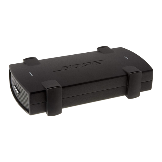
Product Description The PackLite Model A1 power amplifier is a small, lightweight, powerful, and easy-to-use amplifier that interfaces quickly with the Bose PS1 power stand and B1 bass modules to ® provide high bass output for demanding instruments such as bass guitar and drums. The con- nections are quick and easy: plug in the AC cord, connect the A1 to the PS1 power stand, and play. -
Page 4: Amplifier Rear Panel Connections And Controls
Amplifier Rear Panel Connections and Controls 1 - AC power connector: Accommodates the supplied AC power cord to connect your amplifier to the appropriate AC (mains) outlet. Check the product label of your amplifier for the voltage rating: 120V or 220-240V. 2 - Power switch: In the ON (l) position, applies power to your amplifier. -
Page 5: Setting Up A Single A1 Amplifier
Setting Up a Single A1 Amplifier The A1 amplifier is designed to add more bass output to a system that already has two B1 bass modules connected to the Amp 3 OUT connector on the PS1 power stand. The A1 amplifier can power up to two additional B1 bass modules. -
Page 6: Using Multiple A1 Amplifiers
Using Multiple A1 Amplifiers To add more bass capability to your system, you can connect multiple A1 amplifiers as shown below. 1. Connect the AC power cord to an AC (mains) outlet. 2. Make sure the Power switch is OFF. 3. -
Page 7: Using The A1 In Other Applications
Using the A1 in other applications The A1 amplifier can be used as a power amplifier in other system configurations. The A1 can drive other passive loudspeakers including subwoofers, floor monitors, studio monitors, and guitar cabinets. The A1 can amplify a balanced or unbalanced signal from a line- level device, such as a mixing console, and drive any loudspeaker load (4-ohm minimum) that is capable of handling 250W. -
Page 8: Specifications
Specifications Electrical Power, 4-ohm load: 250 watts RMS (1 kHz, 0.1% THD) Power, 8-ohm load: 125 watts RMS (1 kHz, 0.1% THD) Minimum loudspeaker load: 4 Ohms Signal to noise: 100 dB (20 Hz to 20 kHz) Voltage gain: 30 dB Input sensitivity: 1.15 V (+3.4 dBu) Input sensing:... -
Page 9: Production Notes
PRODUCTION NOTES The PackLite A1 amplifier has been manufactured in two versions, a 120V version (product code 039057) and a 220-240V version (product code 039058). The early 120V units, serial numbers 039057Z52620201AC to 039057Z52621200AC, are non- RoHS compliant units. 120V units built after the 5262 Julian date (9/19/2005) are fully RoHS compliant. -
Page 10: Packaging Part List, Packlite Tm A1 Amplifier Assembly (See Figure 1)
PACKAGING PART LIST PackLite A1 Amplifier Assembly (see Figure 1) ® Item Description Bose Part Vendor Part Qty. Note Number Number Number Filler, Sheet, 295x168x6, A=B 291589 1450-8830+0 Owners Manual 287546 4301-7207+0 Sheet, Warranty / Welcome 287553 3050-3681 Carry Bag, Nylon 280x150x70... -
Page 11: Main Part List, Packlite A1 Amplifier Assembly (See Figure 2)
HOUSING, CHASSIS, UPPER, 1405-6801+0 ALUM, 266x140x28mm INPUT SIGNAL AND LIMITING LED PCB- 2, 4 PCB ASSY, BS91C21+LED2 (PART OF INPUT/LIMITER PCB) BOSE LOGO, ALUM, 40x9.8x1.3mm 288677 2150-7161+0 FRONT GRILLE, PERFORATED 288675 1405-6901+0 STEEL, 124x48x0.8mm FAN, DC, 12V, 40x40x10mm 291332 8913-0002+0... - Page 12 Figure 2. PackLite A1 Amplifier Exploded View...
-
Page 13: Electrical Part Lists
ELECTRICAL PART LIST Power Supply / Amplifier PCB Assembly Resistors Reference Description Vendor Part Note Designator Number 1K, RMG, 0603/1608, 1/16W, 1% 4723-102A+P 1K, RMG, 0603/1608, 1/16W, 1% 4723-102A+P 10K, RMG, 0603/1608, 1/16W, 1% 4723-103A-P 1K, RMG, 0603/1608, 1/16W, 1% 4723-102A+P 4.7K, RMG, 0603/1608, 1/16W, 1% 4723-472A-P... - Page 14 ELECTRICAL PART LIST Power Supply / Amplifier PCB Assembly Resistors (continued) Reference Description Vendor Part Note Designator Number 47K, RMG, 0603/1608, 1/16W, 1% 4723-473A-P 47K, RMG, 0603/1608, 1/16W, 1% 4723-473A-P 1.8K, RMG, 0603/1608, 1/16W, 1% 4723-182A-P 1K, RMG, 0603/1608, 1/16W, 1% 4723-102A+P 1K, RMG, 0603/1608, 1/16W, 1% 4723-102A+P...
- Page 15 ELECTRICAL PART LIST Power Supply / Amplifier PCB Assembly Resistors (continued) Reference Description Vendor Part Note Designator Number R103 820K, RMG, 0805, 1/10W, 5% 4720-824J-J R104 820K, RMG, 0805, 1/10W, 5% 4720-824J-J R105 82K, RMG, 0805, 1/10W, 5% 4720-823J-J R106 82K, RMG, 0805, 1/10W, 5% 4720-823J-J R200...
- Page 16 ELECTRICAL PART LIST Power Supply / Amplifier PCB Assembly Resistors (continued) Reference Description Vendor Part Note Designator Number R233 36K, RMG, 0603, 1/16W, 1% 4723-363A+P R234 10K, RMG, 0603/1608, 1/16W, 1% 4723-103A-P R236 10K, RMG, 0603/1608, 1/16W, 1% 4723-103A-P R238 36K, RMG, 0603, 1/16W, 1% 4723-363A+P R239...
- Page 17 ELECTRICAL PART LIST Power Supply / Amplifier PCB Assembly Capacitors (continued) Reference Description Vendor Part Note Designator Number 2.2uF, CC, 1206, 50V, 10%, X7R, MURATA 150F-225K+6-CFM 2.2uF, CC, 1206, 50V, 10%, X7R, MURATA 150F-225K+6-CFM 1uF, 1206, X7R, CC, 50V, 10%, MURATA 150F-105K+6-CFM (NON-ROHS UNITS) 2.2uF, CC, 1206, 50V, 10%, X7R, MURATA...
- Page 18 ELECTRICAL PART LIST Power Supply / Amplifier PCB Assembly Capacitors (continued) Reference Description Vendor Part Note Designator Number 220pF, CTC, 0603, 0/60, 5%, 0.8X1.6 15CH-221J+P-AC 220pF, CTC, 0603, 0/60, 5%, 0.8X1.6 15CH-221J+P-AC 220pF, CTC, 0603, 0/60, 5%, 0.8X1.6 15CH-221J+P-AC 1000pF, CTC, 0805, 0/30, 5%, 1.2x2.5 15CG-102J-J-BD 0.1uF, CC, 0603/1608, 50V, 10%, 1x2 150F-104K-P-AC...
- Page 19 ELECTRICAL PART LIST Power Supply / Amplifier PCB Assembly Capacitors (continued) Reference Description Vendor Part Note Designator Number C212 470pF, CC, 2211, 250VAC, 10%, 2.8X5.7 150R-471K+Y-EKZ 3, 4 C213 470pF, CC, 2211, 250VAC, 10%, 2.8X5.7 150R-471K+Y-EKZ 3, 4 C214 100pF, CC, 0603/1608, 50V, 5%, 1X2 150F-101J-P-AC C215 100pF, CC, 0603/1608, 50V, 5%, 1X2...
- Page 20 ELECTRICAL PART LIST Power Supply / Amplifier PCB Assembly Diodes Reference Description Vendor Part Note Designator Number BAS321, 200V, 250MA, 50NS, SOD323 480S-3210+3 BAS321, 200V, 250MA, 50NS, SOD323 480S-3210+3 BAS321, 200V, 250MA, 50NS, SOD323 480S-3210+3 BAS321, 200V, 250MA, 50NS, SOD323 480S-3210+3 BAS321, 200V, 250MA, 50NS, SOD323 480S-3210+3...
- Page 21 4903-6820+3 ® 32A, TO-252AA (Bose part number 291330) FDD368, MOSFET, N-CHANNEL, 2_NL, 100V, 4903-6820+3 32A, TO-252AA (Bose part number 291330) FDD368, MOSFET, N-CHANNEL, 2_NL, 100V, 4903-6820+3 32A, TO-252AA (Bose part number 291330) FDD368, MOSFET, N-CHANNEL, 2_NL, 100V, 4903-6820+3 32A, TO-252AA (Bose part number 291330)
- Page 22 ELECTRICAL PART LIST Power Supply / Amplifier PCB Assembly Miscellaneous Reference Description Vendor Part Note Designator Number F100 FUSE, T6.3A/125V, TE5-T, PSE/UL 5120-1094+0 3, 4 (120V UNITS) F100 FUSE, T3.15A, 250V, 8.5X8, VDE/UL/SEMKO, 5120-0087+0 3, 4 TR5-T (220-240V UNITS) F200 0 OHM, RMG, 1206, 1/8W, 1% 4721-000A+6 3, 4...
- Page 23 ELECTRICAL PART LIST Input / Limiter PCB Assembly Resistors Reference Description Vendor Part Note Designator Number R301 39K, RMG, 0805, 1/10W, 1% 4720-393A+J R302 39K, RMG, 0805, 1/10W, 1% 4720-393A+J R303 24K, RMG, 0805, 1/10W, 5% 4720-243J+J R304 100 OHM, RMG, 0805, 1/10W, 5% 4720-101J+J R305 10K, RMG, 0805, 1/10W, 5%...
- Page 24 ELECTRICAL PART LIST Input / Limiter PCB Assembly Resistors (continued) Reference Description Vendor Part Note Designator Number R348 2.7K, RMG, 0805, 1/10W, 1% 4720-272A+J R349 750K, RMG, 0805, 1/10W, 5% 4720-754J+J R350 30K, RMG, 0805, 1/10W, 1% 4720-303A+J R351 0 OHM, RMG, 0805, 1/10W, 5% 4720-000J+J R352 51 OHM, RCF, 1/4W, 5%, AT...
- Page 25 ELECTRICAL PART LIST Input / Limiter PCB Assembly Capacitors (continued) Reference Description Vendor Part Note Designator Number C319 1000pF, CTC, 0805, 0/30, 5%, 1.2x2.5 15CG-102J+J-BD C320 1000pF, CTC, 0805, 0/30, 5%, 1.2x2.5 15CG-102J+J-BD C321 1000pF, CTC, 0805, 0/30, 5%, 1.2x2.5 15CG-102J+J-BD C322 1000pF, CTC, 0805, 0/30, 5%, 1.2x2.5...
- Page 26 ELECTRICAL PART LIST Input / Limiter PCB Assembly Diodes Reference Description Vendor Part Note Designator Number D301 1N4148T, AT 4804-1480+2 D302 1N4148T, AT 4804-1480+2 D303 1N4148T, AT 4804-1480+2 D304 1N4148T, AT 4804-1480+2 D305 1N4148, AT (NON-ROHS UNITS) 4804-1480-2 D305 ZENER, 12V, 1/2W, 5%, AT, TEMIC 4837-1206+2 (ROHS COMPLIANT UNITS) D306...
- Page 27 ELECTRICAL PART LIST Input / Limiter PCB Assembly Transistors (continued) Reference Description Vendor Part Note Designator Number Q311 2N3904, RLT (NON-ROHS UNITS) 4853-9040-K Q311 2N3904TA, RLT (ROHS COMPLIANT UNITS) 4853-9040+K Q312 2N3904, RLT (NON-ROHS UNITS) 4853-9040-K Q312 2N3904TA, RLT (ROHS COMPLIANT UNITS) 4853-9040+K Q313 2N3904, RLT (NON-ROHS UNITS)
-
Page 28: Input / Limiter Pcb Assembly
ELECTRICAL PART LIST Input / Limiter PCB Assembly Miscellaneous (continued) Reference Description Vendor Part Note Designator Number WIRE JUMPER, ROLLER FORM, D=0.6MM 635N-0002+0 WIRE JUMPER, ROLLER FORM, D=0.6MM 635N-0002+0 WIRE JUMPER, ROLLER FORM, D=0.6MM 635N-0002+0 WIRE JUMPER, ROLLER FORM, D=0.6MM 635N-0002+0 WIRE JUMPER, ROLLER FORM, D=0.6MM 635N-0002+0... -
Page 29: Signal Led Pcb Assembly
ELECTRICAL PART LIST Signal LED PCB Assembly Diodes Reference Description Vendor Part Note Designator Number D315 LOW CURRENT LED, SMD, RED, 2mA, 3700-7829+R D316 LOW CURRENT LED, SMD, RED, 2mA, 3700-7829+R D317 LED, OS, GN, LOW CURRENT, 525NM, 0603 3700-7834+G D318 LED, OS, GN, LOW CURRENT, 525NM, 0603 3700-7834+G... -
Page 30: Disassembly Procedures
DISASSEMBLY PROCEDURES The PackLite A1 amplifier is housed in a die-cast metal chassis. It is held together in a clam-shell type configuration using four screws. Note: Refer to the photos at right or Figure 2 for the following information. 1. Top Chassis Housing Removal 1.1 Place the unit, top cover down, onto a soft surface. - Page 31 DISASSEMBLY PROCEDURES 3. Power Supply / Amplifier PCB Assembly Removal 3.1 Perform procedure 1. 3.2 Unplug the input / limiter PCB (9) wiring harnesses from the power supply / amplifier PCB (8) at J301, J302 and J303. 3.3 Unplug the wiring harnesses at CON300 and CON301 on the power supply / amplifier PCB assembly.
- Page 32 DISASSEMBLY PROCEDURES 5. LED PCB Removal 5.1 Perform procedure 1. 5.2 Unplug the wiring harness from the input / limiter PCB (9) for the LED PCB (2 or 19) that you wish to remove. These harnesses unplug from the connector at the LED PCB end of the harness.
- Page 33 Lift out the rear panel. 7. Front Panel Removal 7.1 Perform procedure 1. 7.2 Lift out the front panel (4). Re-assembly Note: Be sure to align the front panel so that the Bose logo is facing ® the correct direction. Test Procedures Required Equipment: 1.3 Measure the DC voltage across the load.
-
Page 34: Test Procedures
TEST PROCEDURES 3.2 Connect the output of the A1 to the 6. Signal to Noise Test 4 Ohm load resistor. 6.1 Remove the signal generator and insert 3.3 Power on the unit. a TRS test plug with a 600 Ohm termination between tip and ring. - Page 35 Figure 3. Amplifier/SMPS PCB (Non-RoHS) Figure 4. Amplifier/SMPS PCB (Non-RoHS) Topside Etch Layout Internal Etch Layer 1 Layout...
- Page 36 Figure 5. Amplifier/SMPS PCB (Non-RoHS) Figure 6. Amplifier/SMPS PCB (Non-RoHS) Internal Etch Layer 2 Layout Bottom Etch Layout...
- Page 37 Figure 7. Amplifier/SMPS PCB (RoHS) Figure 8. Amplifier/SMPS PCB (RoHS) Topside Etch Layout Internal Etch Layer 1 Layout...
- Page 38 Figure 9. Amplifier/SMPS PCB (RoHS) Figure 10. Amplifier/SMPS PCB (RoHS) Internal Etch Layer 2 Layout Bottom Etch Layout...
- Page 39 Figure 11. Input/Limiter PCB (Non-RoHS) Top Figure 12. Input/Limiter PCB (Non-RoHS) Side Etch Layout Bottom Side Etch Layout...
- Page 40 Figure 13. Input/Limiter PCB (RoHS) Figure 14. Input/Limiter PCB (RoHS) Top Side Etch Layout Bottom Side Etch Layout...
-
Page 41: Test Cable Wiring Diagrams
Figure 15. Power/Fault LED PCB Etch Layout Figure 16. Signal/Overload LED PCB Etch Layout Test Cable Wiring Diagrams Twisted-pair wiring 600 OHM, 1/4 WATT RESISTOR CONNECTED 4 Ohm, 250 Watt BETWEEN TIP AND RING load resistor Neutrik Speakon 4-pole plug RING SLEEVE Part List... -
Page 42: Troubleshooting
Troubleshooting Problem What to do Power LED is not • Be sure power switch is ON. lit; the amplifier • Make sure the power cord is fully inserted into the unit and an AC outlet. does not seem to • Be sure the AC outlet is live. Try operating a lamp or other equipment operate. -
Page 43: Theory Of Operation, Packlite Model A1 Amplifier
THEORY OF OPERATION PackLite™ Model A1 Amplifier 1. General Overview The Personalized Amplification System™ family of products currently consists of the PS1 power stand, the L1 Cylindrical Radiator loudspeaker and the B1 bass module. The PS1 power stand ® can power up to two B1 bass modules. This is sufficient for most instruments with the exception of some applications of bass guitar, drums (kick drum) and some types of recorded music playback. - Page 44 THEORY OF OPERATION AC Power Input Filter Section (continued) D100 [B/C3] rectifies the AC signal, which is filtered by C107 [C4] and C108 [B4]. N100 [C3] and N101 [B3] provide in-rush current protection when connected to the AC line. MOV1 [C4] and MOV2 [B4] are for surge protection. SG101 through 104 [B/C2] provide an ESD discharge path to the AC mains around the higher impedance of the coils.
- Page 45 THEORY OF OPERATION Amplifier Section (continued) IC4A and IC4B [D2] provide buffers for the audio input, and provide the ability to accept bal- anced or unbalanced inputs. The PackLite A1 amplifier uses the inputs in an unbalanced configuration. R21, R24, R25, R26 [A/B3] provide resistive dividers to determine the under and over-voltage protection thresholds.
- Page 46 THEORY OF OPERATION 6. Input/Limiter PCB Assembly Note: Refer to the Input/Limiter PCB Schematic Diagram, sheet 1 of 1 for the following. The information inside the brackets [ ] is the schematic grid location on the sheet. The Input/Limiter PCB assembly provides: •...
- Page 47 We require 24 dB of gain in that case. If a user connects to a PS1 using an unbalanced cable, they will lose 6 dB of signal going into the PackLite A1. In that case, U304 [C2] will detect that RING is connected to SHIELD, which is grounded, and, after a few seconds, will increase the gain of U301A [D4] by 6 dB in order to compensate.
- Page 48 THEORY OF OPERATION DC Offsets Because of the DC offsets involved (the RING of the input jack is connected to a DC voltage and will momentarily shift when a plug is inserted into the jack), there can be a clicking sound output from the amp when plugs are inserted or removed from the input jacks, as well as when the gain changes.
- Page 49 THEORY OF OPERATION Fan Control The fan turns on when the signal level is high, rather than using a thermal detector. When the input signal reaches about -10 dBV, the Q305/Q310 [B2] combination will turn on the fan. LED Control The green signal LED will turn on at an input level of about -26 dBV.
- Page 50 THEORY OF OPERATION 7. Protection Mechanism Summary Fault Detection What shuts Indicator Recovery when Notes Fault down Output fault is removed Input Signal Output signal level re: Per channel None Immediate Detection Level 0.865 of amplifier DC threshold tied to Clipping supply DC over/under...
-
Page 51: Integrated Circuit Diagrams
Integrated Circuit Diagrams Pin name Description Vd_check High impedance input for monitoring the positive power stage voltage. This controls the soft clipping circuit and the over and under voltage shut down. Vs_check Same as above for the negative rail. Discharge High impedance output that generates a current in case of an over-voltage condition on the power stage voltages (Vs/Vd). - Page 52 Integrated Circuit Diagrams Pin name Description ZobelSense1 Same as pin 15, but for ch 1. Mod_ch1 Pin for connecting the external loop components. This pin is an op-amp output pin and is connected to the modulation comparator. Pwm-_ch1 The first of two balanced high impedance current comparator output. This output is connected via level shift transistors to the driver.
- Page 53 Integrated Circuit Diagrams Pin No. Pin Function Description Isense1_H Over current sensing_1 for High side Isense2_H Over current sensing_2 for High side Non connection Non connection PWM+ Input plus Input minus SS_EN Safe start enable Blanking Dead time control Negative supply of chip LowDrive Low side Output Vdrive...
-
Page 54: Service Manual Revision History
Service Manual Revision History Date Revision Description of Change Change Driven Pages Level Affected 10/05 Document released at revision 00. Service manual release 3/06 Added theory of operation and IC block Additional 38-48 diagrams information available 7/06 Added RoHS compliant amplifier version RoHS compliance 9, 13-29, information... - Page 55 PackLite Power Amplifier Model A1 (120V and 220-240V versions) Service Manual ©2006 Bose Corporation Reference Number 283300-SM Rev. 02 Electronic Copy Only...
- Page 56 SPECIFICATIONS AND FEATURES SUBJECT TO CHANGE WITHOUT NOTICE Bose Corporation The Mountain Framingham Massachusetts USA 01701 P/N: 283300-SM Rev. 02; 7/2006 (P) http://serviceops.bose.com...
Need help?
Do you have a question about the PACKLITE A1 and is the answer not in the manual?
Questions and answers