Table of Contents
Advertisement
Quick Links
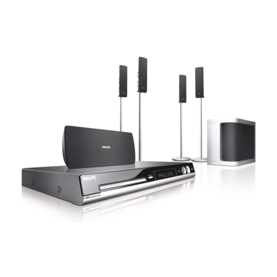
DVD Receiver
CLASS 1
LASER PRODUCT
Contents
1
2
3
4
5
6
7
© Copyright 2005 Philips Consumer Electronics B.V. Eindhoven, The Netherlands.
All rights reserved. No part of this publication may be reproduced, stored in
a retrieval system or transmitted, in any form or by any means, electronic,
mechanical, photocopying, or otherwise without the prior permission of Philips.
Published by KC-TE 0612 AV Systems
Version 1.0
Page
Contents
8
2
4
8
9
11
9
14
17
18
18
19
20
21
21
21
22
23
24
25
26
27
28
Printed in the Netherlands
Subject to modification
HTS3320/51
Page
29
29
30
33
34
35
37
37
38
EN 3139 785 32110
Advertisement
Table of Contents

Related Manuals for Philips HTS3320/51


Summary of Contents for Philips HTS3320/51
-
Page 1: Table Of Contents
Layout: Mono Board (Top View) Layout: Mono Board (Bottom View) © Copyright 2005 Philips Consumer Electronics B.V. Eindhoven, The Netherlands. All rights reserved. No part of this publication may be reproduced, stored in a retrieval system or transmitted, in any form or by any means, electronic, mechanical, photocopying, or otherwise without the prior permission of Philips. -
Page 2: Technical Specifications And Connection Facilities
EN 2 3139 785 32110 Technical Specifications and Connection Facilities LOCATION OF PC BOARDS HTS3320 VERSION VARIA TIONS: HTS3320 Type /Versions: Features & Progressive Scan Line-Out TV-In Aux-In Y/Pb/Pr (YUV) Component Video Output CVBS SCART... - Page 3 3139 785 32110 EN 3 Technical Specifications and Connection Facilities 1. Specifications General: AMPLIFIER: Mains voltage : 230V Output power Mains frequency : 50Hz Front : 100W RMS / channel Power consumption : 150W Rear : 75W RMS / channel <...
-
Page 4: Measurements Setup, Service Aid & Lead Free Requirements
EN 4 3139 785 32110 Measurements Setup, Service Aid & Lead Free Requirements 2. Measurements Setup, Service Aid & Lead Free Requirements MEASUREMENT SETUP Tuner FM Bandpass LF Voltmeter 250Hz-15kHz e.g. PM2534 e.g. 7122 707 48001 RF Generator e.g. PM5326 S/N and distortion meter e.g. - Page 5 3139 785 32110 EN 5 Measurements Setup, Service Aid & Lead Free Requirements SERVICE AIDS Service Tools: Universal Torx driver holder ........4822 395 91019 Torx bit T10 150mm ..........4822 395 50456 Torx driver set T6 - T20 ......... 4822 395 50145 Torx driver T10 extended ........
- Page 6 EN 6 3139 785 32110 Measurements Setup, Service Aid & Lead Free Requirements WAARSCHUWING WARNING Alle IC’s en vele andere halfgeleiders zijn All ICs and many other semi-conductors are gevoelig voor electrostatische ontladingen (ESD). susceptible to electrostatic discharges (ESD). Onzorgvuldig behandelen tijdens reparatie kan Careless handling during repair can reduce life de levensduur drastisch doen verminderen.
- Page 7 Due to lead-free technology some rules have to be respected by the workshop during a repair: • Use only lead-free solder alloy Philips SAC305 with order code 0622 149 00106. If lead-free solder-paste is required, please contact the manufacturer of your solder-equipment.
-
Page 8: 2.2 Service Hints
EN 8 3139 785 32110 Measurements Setup, Service Aid & Lead Free Requirements 2.2 Service Hints CAUTION CHARGED CAPACITORS ON THE SERVO BOARD MAY DAMAGE THE DRIVE ELECTRONICS WHEN CONNECTING A NEW DRIVE.THAT’S WHY, BESIDES THE SAFETY MEASURES LIKE • SWITCH OFF POWER SUPPLY •... -
Page 9: Directions For Use
3. Directions For Use The following except of the Quick Use Guide serves as an introduction to the set. The Complete Direction for the Use can be downloaded in different languages from the internet site of Philips Customer care Center: www.p4c.philips.com... - Page 10 EN 10 3139 785 32110 Directions for Use...
-
Page 11: Dismantling Instructions & Service Positions
3139 785 32110 EN 11 Dismantling Instructions & Service Positions Dismantling Instructions Dismantling of the DVD Loader Tray Cover Dismantling of the Front Board, PSU Module & DVD Loader. 1) Insert a minus screwdriver and push the lever in the direction as shown in Figure 4-1 to unlock the tray before 1) Release 4 snap hooks to remove the Front Board. - Page 12 EN 12 3139 785 32110 Dismantling Instructions & Service Positions Dismantling of the Tuner Module & Mono Board. 1) Loosen 1 screw to remove the Tuner Module. 2) Loosen 2 screws D to remove the Mono Board. Figure 4-5 (AP) Figure 4-6...
- Page 13 3139 785 32110 EN 13 Dismantling Instructions & Service Positions Service Positions Service Position - Front Board Service Position - Mono Board Insulation Sheet Service Position -Amp-Board...
-
Page 14: Service Test Program
EN 14 3139 785 32110 Service Test Program Service Test Program To start service test program refers to Service Mode open the tray with remote control refers to Version or front panel key, while plugging xx refers to Software version number of BEA in the mains cord press 2, 5 8 on (counting up from 01 to 99) remote control, the tray will close... - Page 15 3139 785 32110 EN 15 Service Test Program 5.1.1 Reprogramming of DVD version Matrix 5.1.5 Procedure to check the firmware version to confirm upgrading After repair, the customer setting and region code may be lost. Reprogramming will put the set back in the state in which it has left 1.
- Page 16 EN 16 3139 785 32110 Service Test Program Notes:...
-
Page 17: Block Diagram And Wiring Diagram
Block Diagram, Wiring Diagram 3139 785 32110 EN 17 Block Diagram FL SR SL SW SCART TUNER 1501 TM10 Port_S TU_SCL AMPLIFIER BOARD TU_SDA Analog SW (3139 247 12701) 1 GNDD TU_SD Video Circuit TU_L SCLK GNDD TU_Stereo TU-R MONO BOARD LRCLK NC/RDS +5VL... -
Page 18: Circuit Diagram And Pwb Layout
Circuit Diagram and PWB Layout 3139 785 32110 EN 18 Front: Display 1701 C9 F704 E2 1702 F2 F705 E2 1703 E1 F706 F2 1705 E12 F707 F2 1707 D1 F708 F2 DISPLAY BOARD 1708 G2 F709 F2 1709 A1 F710 F2 +12VL 1710 H7... -
Page 19: Front: Display (Topview)
Circuit Diagram and PWB Layout 3139 785 32110 EN 19 Front: Display (topview) DisplayBd_Topview_33872.pdf_2006-04-05... -
Page 20: Front: Display (Bottom View)
Circuit Diagram and PWB Layout 3139 785 32110 EN 20 Front: Display (Bottom view) DisplayBd_Bottomview_33872.pdf_2006-04-05... -
Page 21: Front: Standby
Circuit Diagram and PWB Layout 3139 785 32110 EN 21 Front: Standby Front: Standby (Top View) Front: Standby (Bottom View) 1801 A2 1802 A1 2801 B1 3801 A2 6801 B2 1801 1802 SKQNAB 3801 470R B3B-EH-A StandbyBoard_Bottomview_33862.pdf_2006-04-05 StandbyBoard_Topview_33862.pdf_2006-04-05 3139_243_33862_a4_sh130_sh1.pdf 2005-12-15... -
Page 22: Mono Board: Circuit Diagram (Part 1)
Circuit Diagram and PWB Layout 3139 785 32110 EN 22 Mono Board: Circuit Diagram (Part 1) 1101 D1 2241 I7 6100 I10 1102 G1 2242 I8 6105 A1 +S_V33 1103 H1 2243 I8 6106 A1 B_Cb 1105 I9 2245 I9 7102 A2 +4.5V 1108 I10... -
Page 23: Mono Board: Circuit Diagram (Part 2)
Circuit Diagram and PWB Layout 3139 785 32110 EN 23 Mono Board: Circuit Diagram (Part 2) 1201 C10 T222 C9 1202 C10 T236 A3 2110 C8 T237 B2 +3V3_D +3V3_D 2252 A3 T238 F3 2253 B3 T240 D6 2280 2279 2254 B3 +3V3_D 7207... -
Page 24: Mono Board: Circuit Diagram (Part 3)
Circuit Diagram and PWB Layout 3139 785 32110 EN 24 Mono Board: Circuit Diagram (Part 3) 1300 A1 3364 I6 1301 C1 3365 A9 1302 F1 3366 A10 1303 G1 3368 B9 1304 H1 4300 C3 2306 A2 4301 D3 2307 C2 4302 D10 2308 C6... -
Page 25: Mono Board: Circuit Diagram (Part 4)
Circuit Diagram and PWB Layout 3139 785 32110 EN 25 Mono Board: Circuit Diagram (Part 4) 1400 B1 F405 B4 1401 E1 F406 C4 1402 C1 F407 C4 1403 B4 F408 B3 2400 A4 F411 D2 2401 F4 F412 E2 4403 +5VL 2402 A3... -
Page 26: Mono Board: Circuit Diagram (Part 5)
Circuit Diagram and PWB Layout 3139 785 32110 EN 26 Mono Board: Circuit Diagram (Part 5) 1501-1 B12 1501-2 E12 1502 G12 2500 B2 2501 B13 2502 B10 2503 B13 2504 B10 For Scart version only 2505 C13 2506 C13 SCART 1 2507 C13 2508 D13... -
Page 27: Layout: Mono Board (Topview)
Circuit Diagram and PWB Layout 3139 785 32110 EN 27 Layout: Mono Board (Topview) MonoBd_TopView_33803.pdf_2006-04-05... -
Page 28: Layout: Mono Board (Bottom View)
Circuit Diagram and PWB Layout 3139 785 32110 EN 28 Layout: Mono Board (Bottom view) MonoBd_BottomView_33803.pdf_2006-04-05... -
Page 29: Overview - Modulator, Input/Output And Headphone/Line Output Connectors
Overview - Modulator, Input/Output and Headphone/Line Output 3139 785 32110 EN 29 Connectors For information only (Amp Board) TAS5508-5142V6REF2 +3.3V 100nF 100nF PVDD CHANNEL 1-2 PWM_A PVDD GVDD PWM_B PWM_C GVDD PWM_D CH1+ OUT_A CH1- OUT_B TP22 TP22 J101 J101 CH 1 SPEAKER OUTPUT TP23... -
Page 30: Power Output Stage (Btl)
Overview - Modulator, Input/Output and Headphone/Line Output 3139 785 32110 EN 30 Connectors For information only (Amp Board) POWER OUTPUT STAGE (BTL) L170 L170 C113 C113 100nF 100nF 0603 0603 PVDD L171 L171 C115 C115 100nF 100nF 0603 0603 GVDD L130 L130 10uH... - Page 31 Overview - Modulator, Input/Output and Headphone/Line Output 3139 785 32110 EN 31 Connectors For information only (Amp Board) POWER OUTPUT STAGE (BTL) L270 L270 C213 C213 100nF 100nF 0603 0603 PVDD L271 L271 C215 C215 100nF 100nF 0603 0603 GVDD L230 L230 10uH...
- Page 32 Overview - Modulator, Input/Output and Headphone/Line Output 3139 785 32110 EN 32 Connectors For information only (Amp Board) POWER OUTPUT STAGE (BTL) L370 L370 C313 C313 100nF 100nF 0603 0603 PVDD L371 L371 C315 C315 100nF 100nF 0603 0603 GVDD L330 L330 10uH...
-
Page 33: Power Supplies
Overview - Modulator, Input/Output and Headphone/Line Output 3139 785 32110 EN 33 Connectors POWER SUPPLIES PVDD C950 C950 C951 C951 C952 C952 C953 C953 C954 C954 C955 C955 R901 R901 100nF 100nF 10nF 10nF 100nF 100nF 10nF 10nF 100nF 100nF 10nF 10nF 0603... -
Page 34: Amp Board Layout : Topview
Overview - Modulator, Input/Output and Headphone/Line Output 3139 785 32110 EN 34 Connectors Amp Board Layout : Topview Pg4_A774_PCB_004 (2.00).pdf_Topview_031806... -
Page 35: Amp Board Layout : Bottomview
Overview - Modulator, Input/Output and Headphone/Line Output 3139 785 32110 EN 35 Connectors Amp Board Layout : Bottomview hts3105ampbdbtm.pdf_Bottomview_031806... - Page 36 Overview - Modulator, Input/Output and Headphone/Line Output 3139 785 32110 EN 36 Connectors For Information Only PSU Module...
-
Page 37: Exploded View & Spare Parts List
Exploded View & Spare Parts List 3139 785 32110 EN 37 Exploded View of the Set Figure 9-1... -
Page 38: Spare Part List
EN 38 3139 785 32110 Exploded View & Spare Parts List HTS3320/51 MISCELLANEOUS 0110 3139 244 12111 COVER CD TRAY HTS3320/51 0185 4822 532 60948 BUSH 0231 3139 244 11011 COVER FAN HTS3105 0331 2422 076 00546 FM AERIAL 24AWG BK B...
Need help?
Do you have a question about the HTS3320/51 and is the answer not in the manual?
Questions and answers