Philips HTS3500K/51 Service Manual

Philips HTS3500K/51 Service Manual

Hide thumbs Also See for HTS3500K/51:

Advertisement

Quick Links

DVD Receiver
Contents
1
2
3
4
5
6
7
8
© Copyright 2005 Philips Consumer Electronics B.V. Eindhoven, The Netherlands.
All rights reserved. No part of this publication may be reproduced, stored in
a retrieval system or transmitted, in any form or by any means, electronic,
mechanical, photocopying, or otherwise without the prior permission of Philips.
Published by KC-TE 0749 AV Systems
Version 1.1
Contents
Page
9
2
4
8
12
14
16
17
18
19
19
20
21
22
23
24
25
26
27
28
29
30
31
32
33
34
Printed in the Netherlands
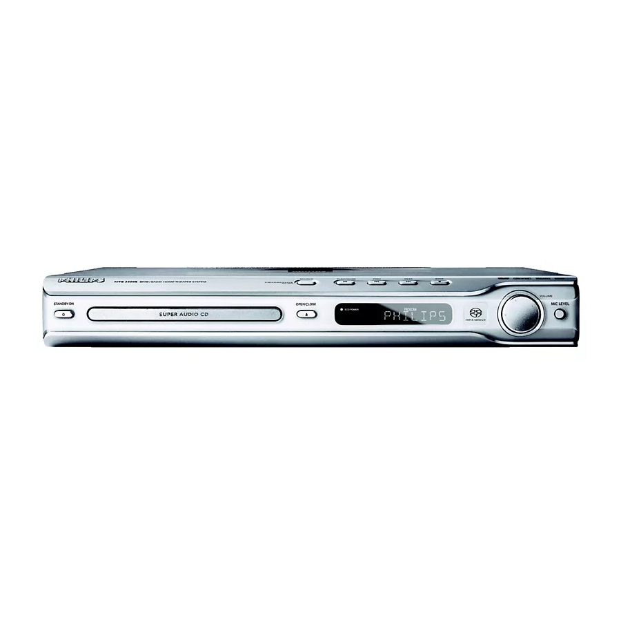
HTS3500K
& HTS5310K
/
51
Subject to modification
/
51
Page
35
35
36
EN 3139 785 31641

Advertisement

Table of Contents
loading

Summary of Contents for Philips HTS3500K/51

  • Page 1: Table Of Contents

    Layout: Mono Board (Bottom View) PSU Circuit Diagram © Copyright 2005 Philips Consumer Electronics B.V. Eindhoven, The Netherlands. All rights reserved. No part of this publication may be reproduced, stored in a retrieval system or transmitted, in any form or by any means, electronic, mechanical, photocopying, or otherwise without the prior permission of Philips.
  • Page 2: Technical Specifications And Connection

    EN 2 3139 785 31640 Technical Specifications and Connection Facilities LOCATION OF PC BOARDS HTS3500K/HTS5310K VERSION VARIATIONS: HTS3300K & HTS3610k HTS3500K & HTS5310k Video (Yellow, Cinch) Component Video Output, (Y/Pb/Pr) Digital In - Coaxial TV In (Left/Right) Auxiliary (Left/Right) Line out (Audio) S-Video Output Progessive Scan...
  • Page 3 3139 785 31640 EN 3 Technical Specifications and Connection Facilities 1. Specifications General: AMPLIFIER: Mains voltage : 230V Output power Mains frequency : 50Hz Front : 100W RMS / channel Power consumption : 100W Rear : 75W RMS / channel <...
  • Page 4: Lead Free Requirements

    EN 4 3139 785 31640 Measurements Setup, Service Aid & Lead Free Requirements 2. Measurements Setup, Service Aid & Lead Free Requirements MEASUREMENT SETUP Tuner FM Bandpass LF Voltmeter 250Hz-15kHz e.g. PM2534 e.g. 7122 707 48001 RF Generator e.g. PM5326 S/N and distortion meter e.g.
  • Page 5 3139 785 31640 EN 5 Measurements Setup, Service Aid & Lead Free Requirements SERVICE AIDS Service Tools: Universal Torx driver holder ........4822 395 91019 Torx bit T10 150mm ..........4822 395 50456 Torx driver set T6 - T20 ......... 4822 395 50145 Torx driver T10 extended ........
  • Page 6: Class 1

    EN 6 3139 785 31640 Measurements Setup, Service Aid & Lead Free Requirements WAARSCHUWING WARNING Alle IC’s en vele andere halfgeleiders zijn All ICs and many other semi-conductors are gevoelig voor electrostatische ontladingen (ESD). susceptible to electrostatic discharges (ESD). Onzorgvuldig behandelen tijdens reparatie kan Careless handling during repair can reduce life de levensduur drastisch doen verminderen.
  • Page 7: Lead Free Requirements

    Due to lead-free technology some rules have to be respected by the workshop during a repair: • Use only lead-free solder alloy Philips SAC305 with order code 0622 149 00106. If lead-free solder-paste is required, please contact the manufacturer of your solder-equipment.
  • Page 8: Direction For Use

    3. Directions For Use The following except of the Quick Use Guide serves as an introduction to the set. The Complete Direction for the Use can be downloaded in different languages from the internet site of Philips Customer care Center: www.p4c.philips.com...
  • Page 9 Once complete, use S / T to select a preset radio station. Note: LINE OUT will output sound only when the speakers volume are reduced to level 1 and below. NEEDS HELP? Visit our website www.philips.com/support HTS3500K-51-QUG_19191 9/15/05, 10:49 AM...
  • Page 10 EN 10 3139 785 31640 Directions For Use...
  • Page 11 3139 785 31640 EN 11 Directions For Use...
  • Page 12: Dismantling Instructions & Service Positions

    EN 12 3139 785 31640 Dismantling Instructions & Service Positions...
  • Page 13 3139 785 31640 EN 13 Dismantling Instructions & Service Positions 4.3 Service Positions Front Board Thick Insulation Sheet Mono Board PSU Board DVD Loader Thick Insulation Sheet...
  • Page 14: Service Test Program

    EN 14 3139 785 31640 Service Test Program Service Test Program To start service test program refers to Service Mode open the tray with remote control refers to Version or front panel key, while plugging xx refers to Software version number of BEA in the mains cord press 2, 5 8 on (counting up from 01 to 99) remote control, the tray will close...
  • Page 15 Service Test Program 3139 785 31640 EN 15 5.1.4 Procedure to upgrade the firmware 5.1.1 Reprogramming of DVD version Matrix After repair, the customer setting and region code may be lost. 1. Power up the set and open tray. Reprogramming will put the set back in the state in which it has left 2.
  • Page 16: Ftd Display Pin Connection

    EN 16 3139 785 31640 FTD Display Pin Connection FTD Display Pin Connection...
  • Page 17: Block Diagram

    Block Diagram, Wiring Diagram 3139 785 31640 EN 17 Block Diagram LINE TV IN FRONT SURR SURR FRONT SUB_ CENTER LEFT RIGHT RIGHT WOOFER LEFT 1501 1502 7662 +9.1V AM / FM SAA6581T RDS_Mux Tuner TM10 RDS IC RIGHT 2422 542 00014 LEFT RDS_CK RDS_DA...
  • Page 18: Wiring Diagram

    Block Diagram, Wiring Diagram 3139 785 31640 EN 18 Wiring Diagram 8001 313911103781(FFC FOIL 10P/120/10P AD FOLD) Port-s SCART TU_SCL TU_SDA 1800 1802 1806 1502 1501 1401 1400 TU_SD 2P EH TO FAN TU_L TUNER TU_Stereo TM10 TU_R NC/RDS Mono board( AV+MPEG+AMP) 3139 243 31471 141X382 FR4 2-layer 11P FFC TO TUNER 10P EH TO PSU...
  • Page 19: Circuit Diagram And Pwb Layout

    Circuit Diagram and PWB Layout 3139 785 31640 EN 19 Front: Display 1701 C8 6717 G6 1702 F2 6718 H8 1703 E1 6719 H8 1705 G3 6720 I8 1707 D1 7701 I2 1708 G7 7702-1 B4 DISPLAY BOARD 1709 B1 7702-2 B6 1710 H5 7703 C3...
  • Page 20: Front: Display (Topview)

    Circuit Diagram and PWB Layout 3139 785 31640 EN 20 Front: Display (topview) Topview_DisplayBd_35766.pdf 2005-11-02...
  • Page 21: Front: Display (Bottom View)

    Circuit Diagram and PWB Layout 3139 785 31640 EN 21 Front: Display (Bottom view) BottomView_DisplayBd_35766.pdf 2005-11-02...
  • Page 22: Front: Standby

    Circuit Diagram and PWB Layout 3139 785 31640 EN 22 Front: Standby Front: Standby (topview) 1900 A1 1901 A1 2901 B1 2902 B1 F901 A1 F902 A1 1901 1900 F901 F902 SKQNAB B2B-EH-A TopView_StandbyBd_35776.pdf 2005-11-02 Front: Standby (Bottom view) 3139_113_35776_a4_sh130_sh1.pdf 2005-05-18 BottomView_StandbyBd_35776.pdf 2005-11-02...
  • Page 23: Mono Board: Circuit Diagram (Part 1)

    Circuit Diagram and PWB Layout 3139 785 31640 EN 23 Mono Board: Circuit Diagram (Part 1) 1101 D1 2219 I2 5120 B5 1102 G1 2220 E6 5122 C2 1103 H1 2221 E5 5123 D2 1105 I9 2222 F6 5124 D4 1107 F5 2223 G4 5125 D3...
  • Page 24: Mono Board: Circuit Diagram (Part 2)

    Circuit Diagram and PWB Layout 3139 785 31640 EN 24 Mono Board: Circuit Diagram (Part 2) 2252 A4 2253 C4 2254 C4 2255 C4 2256 C4 2257 C4 2258 C4 2259 D10 2260 D11 3200 2261 D10 RDS_DAT RDS_DAT 2262 D10 2263 D11 2264 D7 RDS_CLK...
  • Page 25: Mono Board: Circuit Diagram (Part 3)

    Circuit Diagram and PWB Layout 3139 785 31640 EN 25 Mono Board: Circuit Diagram (Part 3) 1300 B9 7302-5 C11 1301 D9 7302-6 D8 1302 G2 7305 D5 1305 D9 7306 C10 2301 B8 7307 E5 2302 B10 7308 E9 2303 B8 7309 G12 2304 B12...
  • Page 26: Mono Board: Circuit Diagram (Part 4)

    Circuit Diagram and PWB Layout 3139 785 31640 EN 26 Mono Board: Circuit Diagram (Part 4) 1401 G9 F405 E8 1402 C9 F406 E8 1403 F9 F407 E8 2400 1404 D9 F409 H8 2314 H6 F410 I7 2400 A5 F411 I7 2401 2402 2401 A5...
  • Page 27: Mono Board: Circuit Diagram (Part 5)

    Circuit Diagram and PWB Layout 3139 785 31640 EN 27 Mono Board: Circuit Diagram (Part 5) 1500 D1 1501 H1 1502 F1 1506 G1 2500 A7 2501 A9 2502 C2 2504 C6 2520 2505 A2 2522 2506 F6 100p F502 3500 100p 2507 G3...
  • Page 28: Mono Board: Circuit Diagram (Part 6)

    Circuit Diagram and PWB Layout 3139 785 31640 EN 28 Mono Board: Circuit Diagram (Part 6) 2110 I12 4602 A4 2601 C3 5604 A7 2602 C4 5605 G5 2603 I8 5606 I5 2610 H10 7613-1 B13 2614 B13 7613-2 C13 2615 B6 7615 A5 2616 B13...
  • Page 29: Mono Board: Circuit Diagram (Part 7)

    Circuit Diagram and PWB Layout 3139 785 31640 EN 29 Mono Board: Circuit Diagram (Part 7) 2701 E4 T713 I8 2702 F5 T714 I9 2703 F1 2704 F2 2705 F3 2706 F3 2707 F4 2712 3752 T703 2712 A8 FE_Left FE_Left 2713 A8 680R...
  • Page 30: Mono Board: Circuit Diagram (Part 8)

    Circuit Diagram and PWB Layout 3139 785 31640 EN 30 Mono Board: Circuit Diagram (Part 8) 1800 B12 1802-A E12 1802-B F12 1802-C G12 1806 G12 1807 H12 2803 B2 2815 C13 2816 C13 For Scart version only 2817 C13 2818 D13 2819 D11 T816...
  • Page 31: Mono Board: Circuit Diagram (Part 9)

    Circuit Diagram and PWB Layout 3139 785 31640 EN 31 Mono Board: Circuit Diagram (Part 9) 1900 A1 1901 D2 2900 D4 2902 B5 2911 A1 2912 B1 2913 A2 7901 2913 2914 B3 LD1117DT 2916 B3 F900 100p T903 2918 C3 +3V3 +3V3...
  • Page 32: Layout: Mono Board (Topview)

    Circuit Diagram and PWB Layout 3139 785 31640 EN 32 Layout: Mono Board (Topview) TopView_MonoBd_31485.pdf 2005-11-02...
  • Page 33: Layout: Mono Board (Bottom View)

    Circuit Diagram and PWB Layout 3139 785 31640 EN 33 Layout: Mono Board (Bottom view) BottomView_MonoBd_31485.pdf 2005-11-02...
  • Page 34: Psu Circuit Diagram

    Circuit Diagram and PWB Layout 3139 785 31640 EN 34 PSU Circuit Diagram (For information only) PSU 04-01-Circuit Diagram 1702 04.11.01.pdf_052005...
  • Page 35: Technical Specifications And Connection 9 Exploded View & Spare Parts List

    Exploded View & Spare Parts List 3139 785 31640 EN 35 Exploded View of the Set Figure 9-1...
  • Page 36: Measurements Setup, Service Aid & Spare Part List

    EN 36 3139 785 31640 Exploded View & Spare Parts List HTS3500K/51 CAPACITORS MISCELLANEOUS 2443 2238 600 15614 CER2 0805 X7R 100V 220P PM10 R 2447 2238 600 15614 CER2 0805 X7R 100V 220P PM10 R 0110 3139 244 06051...
  • Page 37 Exploded View & Spare Parts List 3139 785 31640 EN 37 DIODES PCBA FRONT HTS3000S ROW 6308 4822 130 11397 BAS316 1010 3139 118 58502 PCBA DISPLAY HTS3000S AP 6309 4822 130 11397 BAS316 1020 3139 118 58492 PCBA STAND-BY KEY HTS3000S 6500 4822 130 11397 BAS316 6501 9322 159 70685...
  • Page 38 EN 38 3139 785 31640 Exploded View & Spare Parts List HTS5310K/51 CAPACITORS MISCELLANEOUS 2443 2238 600 15614 CER2 0805 X7R 100V 220P PM10 R 2447 2238 600 15614 CER2 0805 X7R 100V 220P PM10 R 0110 3139 244 06051 COVER CD TRAY CHROME 2454 2020 021 91431 ELCAP YXA 100V S 22U PM20...
  • Page 39 Exploded View & Spare Parts List 3139 785 31640 EN 39 DIODES PCBA FRONT HTS3000S ROW 6308 4822 130 11397 BAS316 1010 3139 118 58502 PCBA DISPLAY HTS3000S AP 6309 4822 130 11397 BAS316 1020 3139 118 58492 PCBA STAND-BY KEY HTS3000S 6500 4822 130 11397 BAS316 6501 9322 159 70685...

This manual is also suitable for:

Hts5310k/51Hts3300kHts5310Hts3500kHts3610kHts5310k

Table of Contents