Table of Contents
Advertisement
Quick Links
DVD Receiver
Service
Service
Service
Service
Service
Service Manual
©
Copyright 2006 Philips Consumer Electronics B.V. Eindhoven, The Netherlands
All rights reserved. No part of this publication may be reproduced, stored in a retrieval system or
transmitted, in any form or by any means, electronic, mechanical, photocopying, or otherwise
without the prior permission of Philips.
Published by HY-ET0619 Service Audio Printed in The Netherlands Subject to modification
Version 1.0
TABLE OF CONTENTS
Location of PC Boards ................................................ 1-2
Versions Variation & Package .................................... 1-2
Specifications .............................................................. 1-3
Measurement Setup ................................................... 1-4
Service Aids ................................................................ 1-5
ESD & Safety Instruction ............................................ 1-6
Pb(Lead) Free Solder ................................................. 1-7
Setting Procedure & Repair Instructions ....................... 2
Disassembly Instructions & Service positions .............. 3
Block & Wiring Diagram ................................................ 4
Control Board ................................................................. 5
Main Board .................................................................... 6
Tuner Board ................................................................... 7
Power Board .................................................................. 8
DVD loader .................................................................... 9
Exploded View ............................................................. 10
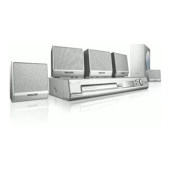
HTS3090
Page
CLASS 1
LASER PRODUCT
GB
/55/77/78
3139 785 32160
Advertisement
Table of Contents

Related Manuals for Philips HTS3090/55/77/78


Summary of Contents for Philips HTS3090/55/77/78
- Page 1 LASER PRODUCT © Copyright 2006 Philips Consumer Electronics B.V. Eindhoven, The Netherlands All rights reserved. No part of this publication may be reproduced, stored in a retrieval system or transmitted, in any form or by any means, electronic, mechanical, photocopying, or otherwise without the prior permission of Philips.
-
Page 2: Location Of Pc Boards
LOCATION OF PC BOARDS TUNER BOARD MAIN BOARD POWER BOARD CONTROL BOARD VERSION VARIATION: Type /Versions HT3090 Features & Board in used /77/78/55 Main PCB (Power Output 200W) Main PCB (DTS-Decoder & Digital OUT) Power Voltage (120-127V / 220-240V ) Composite Video Out &... -
Page 3: Specifications
SPECIFICATIONS MAIN UNIT AMPLIFIER Power Supply Rating: 110–127 V / 220–240 V; Output power: 200 W 50-60 Hz - Front : 30 W / channel Power Consumption: - Rear: 30 W / channel 50 W Dimensions: 360 x 48 x 339 (mm) - Center : 30 W RMS (w x h x d) - Page 4 Select the menu using the " " and " " button on R/C c) TV Show "TUNER AREA" For HTS3090/55/77/78 (LATAM) : setting and the region code may lost. Changing the Region c) Go feature setup page select "PASSWORD". TV show d) Select the tuner area you want by using the "...
-
Page 5: Repair Instructions
REPAIR INSTRUCTIONS... - Page 6 REPAIR INSTRUCTIONS...
-
Page 7: Disassembly Instructions
DISASSEMBLY INSTRUCTIONS Dismantling of the Main PCB 1) Loosen 5 screw "A" at the back panel as shown in figure 4. Dismantling of the Front Panel Assembly 2) Loosen 4 screw " C " on the top of main board as shown in figure 5. -
Page 8: Service Positions
Dismantling of the DVD Module SERVICE POSITIONS Service position A 1) Loosen 4 screws "B" to remove the DVD Module as shown in figure 6. Figure 6 Note: In some service positions the components or copper patterns of one board may risk touching its neighbouring pc Dismantling of the Power Board boards or metallic parts. -
Page 9: Block Diagram
BLOCK DIAGRAM FLASH SDRAM EEPRO M 24C02 MX16M IC 8M X 16 POWER BOARD 74H CU04 Coaxial in DVD MOTOR Drive IC AM5869 EASTWIN LOADER SWITCH POWER M04S SANYO CVBS POWER PCB ASSY230V 100W ES8380CD RF A.B.C.D.E.F MPEG II Decoder DIVX Decoder VIDEO FILTER DOLBY DIGITAL Decoder... -
Page 10: Main Board
WIRING DIAGRAM AUX IN TV IN TUNER BOARD MAIN BOARD POWER BOARD DVD LOADER CONTROL BOARD... -
Page 11: Pin Connection
FTD DISPLAY PIN ASSIGNMENT CONTROL+ STANDBY BOARD TABLE OF CONTENTS FTD Display Pin Assignment ........... 5-1 Circuit Diagram ..............5-2 PCB Layout Top & Bottom View ........5-3 PIN CONNECTION Pin No. Connection Pin No. Connection ## Note ## 1. Fn: Filament pin 2. -
Page 12: Circuit Diagram - Control Board
CIRCUIT DIAGRAM - CONTROL BOARD C301 C302 C303 C304 C305 DP301 C306 C307 C309 C310 C311 C312 C313 C314 C315 C316 C317 C318 C319 C320 C321 C322 C323 C324 C325 C326 C327 C328 C329 C633 C634 C635 D303 D305 D307 DP301 IC301 R301... -
Page 13: Pcb Layout - Top View
PCB LAYOUT - TOP VIEW C311 C317 RB301A A1 RB303 A2 TA301 A3 TA303 A3 TA305 A3 TA308 A1 C312 DP301 A2 RB302 A2 SN301 A2 TA302 A3 TA304 A3 TA306 A1 XL301 A2 PCB LAYOUT - BOTTOM VIEW C301 C305 C310 C316... - Page 14 Internal IC diagram - ES8380FCD Motor DVD/CD Motor Driver MAIN BOARD Video TV Display Audio Speakers SDRAM Audio Microphone In ES8380 (8/16-MB) Phoenix S/P DIF A/V Receiver EEPROM VFD Panel VFD Driver ROM/Flash IR Remote TABLE OF CONTENTS Internal IC Diagram ........... 6-1 Circuit Diagram (Top Left) .........
-
Page 15: Circuit Diagram - Top Left
CIRCUIT DIAGRAM - TOP LEFT C124 C154 C180 C203 C221 C244 C264 C283 C304 C336 C349 C448 C467 C485 C807 C834 FB102 C100 C126 C155 C180 C204 C222 C245 C265 C284 C305 C337 C356 C449 C468 C486 C808 C839 CN102 E1 FB108 C101 C127... -
Page 16: Circuit Diagram - Top Right
CIRCUIT DIAGRAM - TOP RIGHT FB125 FB225 IC209 L110 L802 Q801 R126 R156 R177 R196 R223 R251 R278 R385 R815 R839 R856 ZD108 FB126 FB226 IC209 L111 L803 Q802 R129 R157 R178 R197 R225 R254 R320 R386 R816 R840 R856 ZD110 FB127 FB227... -
Page 17: Circuit Diagram - Bottom Left
CIRCUIT DIAGRAM - BOTTOM LEFT MX29LV160CBTC-70G IC101 ES8380FCD NT5SV8M16DS-6K... -
Page 18: Circuit Diagram - Bottom Right
CIRCUIT DIAGRAM - BOTTOM RIGHT For source change used... - Page 19 PCB LAYOUT - TOP VIEW C100 C157 C210 C249 C300 C466 C487 C813 FB101 FB141 IC209 L111 L806 R107 R149 R173 R193 R225 R257 R305 R333 R832 R922 ZD116 A3 C101 C158 C211 C250 C301 C467 C488 C814 FB102 FB142 IC601 L112 Q101...
- Page 20 PCB LAYOUT - BOTTOM VIEW C139 C182 C198 C236 C261 C276 C286 C318 C343 C406 C448 C458 C831 R389 R399 C102 C143 C183 C238 C262 C277 C288 C327 C345 C407 C449 C459 C832 R390 R400 C103 C145 C185 C204 C239 C263 C278 C291...
- Page 21 VOLTGE IC111 (SN74LVTH273PWR) IC102A (MX29LV800CBTC) Pin NO Voltage 0.00 2.86 1.46 2.42 2.11 1.33 1.20 1.64 0.00 0.00 3.40 5.00 0.00 0.00 0.00 3.40 0.00 1.20 1.95 1.27 Voltage 5.00 1.70 1.70 1.70 1.73 1.73 1.73 3.00 0.00 0.00 1.85 0.00 0.00 1.73...
-
Page 22: Tuner Adjustment Table
TUNER ADJUSTMENT TABLE Waverange Input frequency Input Tuned to Adjust Output Scope/Voltmeter VARICAP ALIGNMENT 108MHz 6.5V 1.2V check 87.5 - 108MHz (50kHz grid) 87.5MHz check 1.0V 0.5V 1602KHz check 7.8V 0.2V T005 1.1V 0.5V 531KHz 530-1710kHz TUNER BOARD (10kHz grid) ( 21L / 21L / 37S ) check 1700KHz... -
Page 23: Circuit Diagram - Tuner Board
CIRCUIT DIAGRAM - TUNER BOARD ANT001 A1 R005 C002 R006 C004 R007 C005 R010 C006 R011 C007 R015 C008 R016 C009 R017 R018 C010 R019 C011 R020 C012 R021 C013 R023 C014 R024 C015 R025 C016 R026 C017 R027 C018 R028 C019 R029... -
Page 24: Pcb Layout - Tuner Board (Top)
PCB LAYOUT - TUNER BOARD (TOP) ANT001 A2 C009 C025 C047 D002 IF001 A1 JMP4 C1 JMP8 C2 Q001 C2 T002 VC001 VD003 C005 C019 C02A CN001 C1 D003 IF002 B2 JMP5 B2 JMP9 B2 Q002 B2 T003 VC001 VD004 C006 C030 CN002 A1... -
Page 25: Pcb Layout - Tuner Board (Bottom)
PCB LAYOUT - TUNER BOARD (BOTTOM) C001 C014 C021 C036 C041 C050 R002 R010 R019 R025 R030 TIP1 TIP14 B1 TIP4 A2 TIP9 B2 C002 C010 C015 C022 C031 C037 C042 C052 R004 R011 R020 R026 R031 TIP10 A1 TIP15 B1 TIP5 A2 C004 C011... -
Page 26: Power Board
Voltage IC 952 Pin NO Voltage 5.00 5.00 3.48 1.40 1.58 3.49 0.00 13.20 0.45 0.43 13.20 13.20 5.00 5.00 5.00 0.00 IC951 Pin NO Voltage 1.36 5.00 1.50 0.00 13.20 5.00 13.00 12.00 IC902 Pin NO Voltage -13.4 128.00 130.00 131.00 132.00... -
Page 27: Circuit Diagram - Power Board
CIRCUIT DIAGRAM - POWER BOARD BD901 C913 C923 C959 C975 C987 CN951 D4 D954 GT902 B1 L901 Q951 R904 R915 R953 R964 R975 R985 T902 C903 C914 C924 C960 C976 C989 CN952 A3 D955 GT903 C1 L902 Q952 R905 R916 R954 R965 R976... -
Page 28: Dvd Loader
DVD LOADER It is not recommended for component repair on this Module but to replace the major assembly when it becomes defective. Therefore limited service parts list are published in this chapter. -
Page 29: Mechanical Exploded View
10-1 10-1 MECHANICAL EXPLODED VIEW... - Page 30 APE103920-0012 9965 000 40958 CONTROL PCB ASS'Y ABE106370-0001 9965 000 38282 CONTROL PCB ASS'Y (/55 Only) APE106370-0001 9965 000 38278 VOLUME KNOB PHILIPS BPK105093-0002 9965 000 38277 DVD DOOR BPD101125-1001 9965 000 38279 POWER KNOB ABS DR30U0 BPK112109-1001 9965 000 38280...
Need help?
Do you have a question about the HTS3090/55/77/78 and is the answer not in the manual?
Questions and answers