Table of Contents
Advertisement
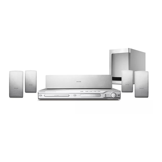
DVD Receiver
CLASS 1
LASER PRODUCT
Contents
1
2
3
4
5
6
7
© Copyright 2006 Philips Consumer Electronics B.V. Eindhoven, The Netherlands.
All rights reserved. No part of this publication may be reproduced, stored in
a retrieval system or transmitted, in any form or by any means, electronic,
mechanical, photocopying, or otherwise without the prior permission of Philips.
Published by HY-TE0623 AV Systems
Version 1.0
Page
2
4
9
11
14
17
17
18
19
20
20
24
25
26
29
30
31
33
34
35
36
36
Printed in the Netherlands
Contents
8
Subject to modification
HTS3440
/
37
Page
37
37
37
38
38
38
39
46
47
48
49
49
50
51
EN 3139 785 31880
Advertisement
Table of Contents

Related Manuals for Philips HTS3440/37


Summary of Contents for Philips HTS3440/37
-
Page 1: Table Of Contents
Layout: Front- Display Board (Top view) Layout: Front- Display Board (Bottom view) © Copyright 2006 Philips Consumer Electronics B.V. Eindhoven, The Netherlands. All rights reserved. No part of this publication may be reproduced, stored in a retrieval system or transmitted, in any form or by any means, electronic, mechanical, photocopying, or otherwise without the prior permission of Philips. -
Page 2: Technical Specifications And Connection Facilities
EN 2 3139 785 31880 Technical Specifications and Connection Facilities LOCATION OF PC BOARDS AV Board PCBAS 9.1 AV Interface Board Tuner Loader HTS3440 PCBAS Front Panel VERSION VARIATIONS: HTS3440 Type /Versions: Features & Progressive Scan Digital-In (Coax) TV-In Aux-In Y/Pb/Pr (YUV) Component Video Output Coax CVBS... - Page 3 3139 785 31880 EN 3 Technical Specifications and Connection Facilities 1. Specifications General: AMPLIFIER: Mains voltage : 120V/230V Output power Mains frequency : 50/60Hz Front : 125W RMS / channel Power consumption : 70W Rear : 125W RMS / channel <...
-
Page 4: Measurements Setup, Service Aid & Lead Free Requirements
EN 4 3139 785 31880 Measurements Setup, Service Aid & Lead Free Requirements 2. Measurements Setup, Service Aid & Lead Free Requirements MEASUREMENT SETUP Tuner FM Bandpass LF Voltmeter 250Hz-15kHz e.g. PM2534 e.g. 7122 707 48001 RF Generator e.g. PM5326 S/N and distortion meter e.g. - Page 5 3139 785 31880 EN 5 Measurements Setup, Service Aid & Lead Free Requirements SERVICE AIDS Service Tools: Universal Torx driver holder ........4822 395 91019 Torx bit T10 150mm ..........4822 395 50456 Torx driver set T6 - T20 ......... 4822 395 50145 Torx driver T10 extended ........
- Page 6 EN 6 3139 785 31880 Measurements Setup, Service Aid & Lead Free Requirements WAARSCHUWING WARNING Alle IC’s en vele andere halfgeleiders zijn All ICs and many other semi-conductors are gevoelig voor electrostatische ontladingen (ESD). susceptible to electrostatic discharges (ESD). Onzorgvuldig behandelen tijdens reparatie kan Careless handling during repair can reduce life de levensduur drastisch doen verminderen.
- Page 7 Due to lead-free technology some rules have to be respected by the workshop during a repair: • Use only lead-free solder alloy Philips SAC305 with order code 0622 149 00106. If lead-free solder-paste is required, please contact the manufacturer of your solder-equipment.
-
Page 8: Service Hints
EN 8 3139 785 31880 Measurements Setup, Service Aid & Lead Free Requirements 2.2 Service Hints CAUTION CHARGED CAPACITORS ON THE SERVO BOARD MAY DAMAGE THE DRIVE ELECTRONICS WHEN CONNECTING A NEW DRIVE.THAT’S WHY, BESIDES THE SAFETY MEASURES LIKE • SWITCH OFF POWER SUPPLY •... -
Page 9: Directions For Use
3. Directions For Use The following except of the Quick Use Guide serves as an introduction to the set. The Complete Direction for the Use can be downloaded in different languages from the internet site of Philips Customer care Center: www.p4c.philips.com... - Page 10 EN 10 3139 785 31880 Directions for Use...
-
Page 11: Dismantling Instructions & Service Positions
3139 785 31880 EN 11 Dismantling Instructions & Service Positions Dismantling Instructions Dismantling of the DVD Loader Tray Cover Dismantling of the Front Board, PSU Module & DVD Loader. 1) Insert a minus screwdriver and push the lever in the direction as shown in Figure 4-1 to unlock the tray before 1) Release 4 snap hooks to remove the Front Board. - Page 12 EN 12 3139 785 31880 Dismantling Instructions & Service Positions Dismantling of the Tuner Module & AV Board. 1) Loosen 1 screw (See Figure 4-5) to remove the Tuner Module. Figure 4-5 2) Loosen 2 screws (See Figure 4-6 & Figure 4-7) to remove the AV Board.
- Page 13 3139 785 31880 EN 13 Dismantling Instructions & Service Positions Service Positions Insulation Sheet PCBA 9.1 AV Board Insulation Sheet Insulation Sheet Service Position - PCBAS 9.1 Service Position - AV Board Front Board Service Position - Amp Board Service Position - Front Board...
-
Page 14: Service Test Program
EN 14 3139 785 31880 Service Test Program Service Test Program To start service test program refers to Service Mode open the tray with remote control refers to Version or front panel key, while plugging xx refers to Software version number of BEA in the mains cord press 2, 5 8 on (counting up from 01 to 99) remote control, the tray will close... - Page 15 3139 785 31880 EN 15 Service Test Program 5.1.1 Reprogramming of DVD version Matrix 5.1.4 Procedure to upgrade the firmware 1. Power up the set and open tray. After repair, the customer setting and region code may be lost. 2. Insert the prepared Upgrade CDROM and close the tray. Reprogramming will put the set back in the state in which it has left 3.
- Page 16 EN 16 3139 785 31880 Service Test Program Notes:...
-
Page 17: Block Diagram, Wiring Diagram
Block Diagram, Wiring Diagram 3139 785 31880 EN 17 Wiring Diagram 1103 1600 1404 NC/RDS NC/RDS TU_R TU_R TU_Stereo TU_Stereo TU_L TU_L 1601 TU_SD TU_SD TU_SDA TU_SDA TU_SCL TU_SCL Port_S Port_S 1504 1105 1500 1501 Wiring Diagram.pdf 2006-04-06... -
Page 18: Block Diagram: Subwoofer
Block Diagram, Wiring Diagram 3139 785 31880 EN 18 Block Diagram: Subwoofer 3440SW_Service_Manual_2.pdf _2006-04-06... -
Page 19: Wiring Diagram: Subwoofer
Block Diagram, Wiring Diagram 3139 785 31880 EN 19 Wiring Diagram: Subwoofer 3440SW_Service_Manual_2.pdf _2006-04-06... -
Page 20: Circuit Diagram And Pwb Layout
Circuit Diagram and PWB Layout 3139 785 31880 EN 20 AV Board: Circuit Diagram (Part 1) 1100 B1 F103 A2 1102 F1 F105 A2 1104 D1 F106 B2 1105 H12 F107 B2 1106 E1 F108 B2 2100 C2 F109 D2 2105 D4 F110 D2 F100... - Page 21 Circuit Diagram and PWB Layout 3139 785 31880 EN 21 AV Board: Circuit Diagram (Part 2) U2 H6 7205 H10 1200 C5 7206 E8 1201 E2 7207-1 H8 1202 G1 F202 G2 3V3D 1203 G2 F203 G2 1204 A6 F204 G2 5203 2214 1204...
- Page 22 Circuit Diagram and PWB Layout 3139 785 31880 EN 22 AV Board: Circuit Diagram (Part 3) 1301-A E13 6330 C12 1301-B F12 6331 C12 1301-C F12 6332 D12 1302 G2 6333 B5 2340 F11 6334 B5 2341 D7 7342 A7 2342 E4 7344 B7 For Scart version only...
- Page 23 Circuit Diagram and PWB Layout 3139 785 31880 EN 23 AV Board: Circuit Diagram (Part 4) 1402 E1 1403 H2 1404 H3 1405 F3 1407 D4 1408 D9 2400 C5 2401 D4 2402 D10 2404 D8 2414 A8 PO_Mute PD_Mute BAS316 2415 B4 4409...
-
Page 24: Layout: Av Board (Top View)
Circuit Diagram and PWB Layout 3139 785 31880 EN 24 Layout: AV Board (Top view) AVBd_Topview_33614.pdf _2006-04-06... -
Page 25: Layout: Av Board (Bottom View)
Circuit Diagram and PWB Layout 3139 785 31880 EN 25 Layout: AV Board (Bottom view) AVBd_Bottomview_33614.pdf _2006-04-06... -
Page 26: Pcba 9.1 Board: Circuit Diagram
Circuit Diagram and PWB Layout 3139 785 31880 EN 26 PCBA 9.1 Board: Circuit Diagram (Part 1) 1101 D1 3111 A12 6105 H6 1102 F1 3112 A8 6106 I12 1103 H1 3113 A12 7104 D4 1104 I10 3115 A12 7105 D3 CENTRE_CH DV33 1105 F5... - Page 27 Circuit Diagram and PWB Layout 3139 785 31880 EN 27 PCBA 9.1 Board: Circuit Diagram (Part 2) 1201 D5 3237 G2 F223 A8 1202 D5 3238 H8 F224 A8 1203 A12 3239 G2 F225 B8 1204 A11 3240 G2 F226 B8 1205 A8 3241 G2 F227 B8...
- Page 28 Circuit Diagram and PWB Layout 3139 785 31880 EN 28 PCBA 9.1 Board: Circuit Diagram (Part 3) 1301 D9 1302 F8 2301 C5 2312 A10 2313 C6 DV33 2314 C7 2315 A9 2333 5303 2320 B7 +5VL 2312 2321 D2 7303-1 100n 2322 E6...
-
Page 29: Layout: Pcba 9.1 Board (Top View)
Circuit Diagram and PWB Layout 3139 785 31880 EN 29 Layout: PCBA 9.1 Board (Top view) PCBA91_Topview_33575.pdf _2006-04-06... -
Page 30: Layout: Pcba 9.1 Board (Bottom View)
Circuit Diagram and PWB Layout 3139 785 31880 EN 30 Layout: PCBA 9.1 Board (Bottom view) PCBA91_Bottomview_33575.pdf _2006-04-06... -
Page 31: Interface Board: Circuit Diagram
Circuit Diagram and PWB Layout 3139 785 31880 EN 31 Interface Board: Circuit Diagram (Part 1) 1600 C1 6107 B13 1601 A1 6108 A8 2101 C5 7100 A4 2102 D5 7101 A7 2103 D9 7102 A8 3100 2104 D12 7103 B7 6104 3101 2105 D9... - Page 32 Circuit Diagram and PWB Layout 3139 785 31880 EN 32 Interface Board: Circuit Diagram (Part 2) 1602 D12 3295 F10 2200 A8 3296 I6 2201 B3 3297 I9 2202 B6 3298 I10 2203 A6 6202 C10 2204 B7 6203 F10 2205 B3 6204 I10 2206 B8...
-
Page 33: Layout: Interface Board (Top View)
Circuit Diagram and PWB Layout 3139 785 31880 EN 33 Layout: Interface Board (Top view) InterfaceBd_Topview_33673.pdf _2006-04-06... -
Page 34: Layout: Interface Board (Bottom View)
Circuit Diagram and PWB Layout 3139 785 31880 EN 34 Layout: Interface Board (Bottom view) InterfaceBd_Bottomview_33673.pdf_2006-04-06... -
Page 35: Front: Display Board
Circuit Diagram and PWB Layout 3139 785 31880 EN 35 Front: Display Board 1501 D13 7508 E6 1502 F2 7509 E10 1504 E1 7510 I2 1507 H6 7511 I12 1508 H6 7512 I12 1509 H7 7513 I13 1510 H7 F702 E2 1511 H7 F703 E2 1512 H7... -
Page 36: Layout: Front- Display Board (Top View)
Circuit Diagram and PWB Layout 3139 785 31880 EN 36 Layout: Front- Display Board (Top view) DisplayBd_Topview_34503.pdf_2006-04-06 Layout: Front- Display Board (Bottom view) DisplayBd_Bottomview_34503.pdf_2006-04-06... -
Page 37: Front: Usb Board
Circuit Diagram and PWB Layout 3139 785 31880 EN 37 Front: USB Board Layout: Front- USB Board (Top view) 1521 A3 2550 B2 3570 A2 5551 A2 F810 A2 F812 A2 1522 A1 2551 A2 3571 A2 5552 A2 F811 A2 F813 A1 WH04D-1 1521... -
Page 38: Front: Standby Board
Circuit Diagram and PWB Layout 3139 785 31880 EN 38 Front: Standby Board Layout: Front- Standby Board (Top view) 1500 B1 1515 B2 1530 B2 2540 B1 2541 B1 F901 B2 F902 B2 StandbyBd_TopView_34523.pdf_2006-04-06 1515 1500 SKQNAB F901 F902 B2B-EH-A Layout: Front- Standby Board (Bottom view) 1530 3139_243_34523_a4_sh130_sh1.pdf... -
Page 39: Amplifier Board (Subwoofer): Circuit Diagram
Circuit Diagram and PWB Layout 3139 785 31880 EN 39 Amplifier Board (Subwoofer): Circuit Diagram (Part 1) 3440SW_Service_Manual_2_pg8.pdf 2006-04-06... - Page 40 Circuit Diagram and PWB Layout 3139 785 31880 EN 40 Amplifier Board (Subwoofer): Circuit Diagram (Part 2) 3440SW_Service_Manual_2_pg9.pdf 2006-04-06...
- Page 41 Circuit Diagram and PWB Layout 3139 785 31880 EN 41 Amplifier Board (Subwoofer): Circuit Diagram (Part 3) 3440SW_Service_Manual_2_pg10.pdf 2006-04-06...
- Page 42 Circuit Diagram and PWB Layout 3139 785 31880 EN 42 Amplifier Board (Subwoofer): Circuit Diagram (Part 4) 3440SW_Service_Manual_2_pg11.pdf 2006-04-06...
- Page 43 Circuit Diagram and PWB Layout 3139 785 31880 EN 43 Amplifier Board (Subwoofer): Circuit Diagram (Part 5) 3440SW_Service_Manual_2_pg12.pdf 2006-04-06...
- Page 44 Circuit Diagram and PWB Layout 3139 785 31880 EN 44 Amplifier Board (Subwoofer): Circuit Diagram (Part 6) 3440SW_Service_Manual_2_pg13.pdf 2006-04-06...
- Page 45 Circuit Diagram and PWB Layout 3139 785 31880 EN 45 Amplifier Board (Subwoofer): Circuit Diagram (Part 7) 3440SW_Service_Manual_2_pg14.pdf 2006-04-06...
-
Page 46: Layout: Amplifier Board (Subwoofer) (Top View)
Circuit Diagram and PWB Layout 3139 785 31880 EN 46 Layout: Amplifier Board (Subwoofer) (Top view) 3440SW_Service_Manual_2_pg15.pdf _2006-04-06... -
Page 47: For Information Only: Psu Module (Subwoofer)
Circuit Diagram and PWB Layout 3139 785 31880 EN 47 For Information Only: PSU module (Subwoofer) 3440SW_Service_Manual_2_pg16.pdf 2006-04-06... -
Page 48: For Information Only: Psu Module (Main Unit)
Circuit Diagram and PWB Layout 3139 785 31880 EN 48 For Information Only: PSU module (Main Unit) PSU06P15-srv1919ww-Circuit.pdf 2006-04-06... -
Page 49: Exploded View & Spare Parts List
Exploded View & Spare Parts List 3139 785 31880 EN 49 Exploded View of the Set Figure 8-1... -
Page 50: Exploded View: Subwoofer
EN 50 3139 785 31880 Exploded View & Spare Parts List Exploded View: Subwoofer Figure 8-2... -
Page 51: Spare Part List
Exploded View & Spare Parts List 3139 785 31880 EN 51 HTS3440/37 SUBWOOF ASSY HTS3440 P (US) MISCELLANEOUS 9965 000 36108 SW3440 SUBWOOFER BOX 9965 000 34997 RUBBER FOOT SW 0110 3139 254 01521 COVER CD TRAY CHROME 0127 3139 244 06011...
Need help?
Do you have a question about the HTS3440/37 and is the answer not in the manual?
Questions and answers