Table of Contents
Advertisement
Quick Links
DVD Receiver
CLASS 1
LASER PRODUCT
Contents
1
2
3
4
5
6
7
© Copyright 2005 Philips Consumer Electronics B.V. Eindhoven, The Netherlands.
All rights reserved. No part of this publication may be reproduced, stored in
a retrieval system or transmitted, in any form or by any means, electronic,
mechanical, photocopying, or otherwise without the prior permission of Philips.
Published by KC-TE 0552 AV Systems
Version 1.0
Page
Contents
8
2
4
9
12
9
14
15
16
16
17
18
19
20
21
22
23
24
25
26
27
Printed in the Netherlands
Headphone/Line Output Connectors
Subject to modification
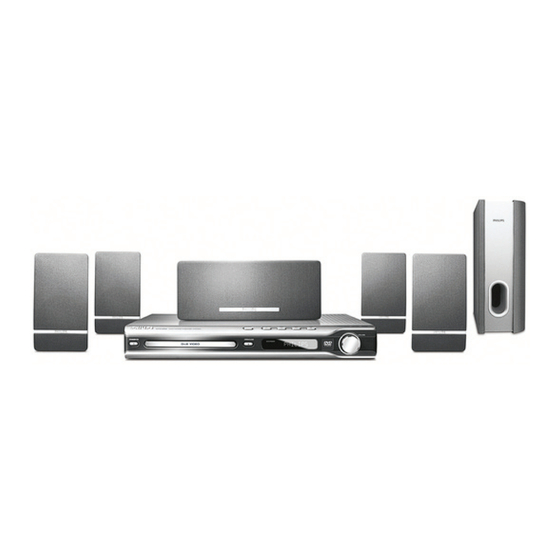
HTS3050
/
16
Page
28
28
29
30
31
33
33
34
EN 3139 785 31790
Advertisement
Table of Contents

Related Manuals for Philips HTS-3050/16


Summary of Contents for Philips HTS-3050/16
-
Page 1: Table Of Contents
Front: Standby PSU Circuit Diagram © Copyright 2005 Philips Consumer Electronics B.V. Eindhoven, The Netherlands. All rights reserved. No part of this publication may be reproduced, stored in a retrieval system or transmitted, in any form or by any means, electronic, mechanical, photocopying, or otherwise without the prior permission of Philips. -
Page 2: Technical Specifications And Connection Facilities
EN 2 3139 785 31790 Technical Specifi cations and Connection Facilities LOCATION OF PC BOARDS HTS3050/16 VERSION VARIATIONS: HTS3050 Type /Versions: Features & Progressive Scan Line-Out TV-In Aux-In Y/Pb/Pr (YUV) Component Video Output Coax CVBS S-Video Output SCART... - Page 3 Technical Specifi cations and Connection Facilities 3139 785 31790 EN 3 1. Specifi cations General: AMPLIFIER: Mains voltage : 230V Output power Mains frequency : 50Hz Front : 100W RMS / channel Power consumption : 70W Rear : 75W RMS / channel <...
-
Page 4: Measurements Setup, Service Aid & Lead Free Requirements
EN 4 3139 785 31790 Measurements Setup, Service Aid & Lead Free Requirements 2. Measurements Setup, Service Aid & Lead Free Requirements MEASUREMENT SETUP Tuner FM Bandpass LF Voltmeter 250Hz-15kHz e.g. PM2534 e.g. 7122 707 48001 RF Generator e.g. PM5326 S/N and distortion meter e.g. - Page 5 Measurements Setup, Service Aid & Lead Free Requirements 3139 785 31790 EN 5 SERVICE AIDS Service Tools: Universal Torx driver holder ........4822 395 91019 Torx bit T10 150mm ..........4822 395 50456 Torx driver set T6 - T20 ......... 4822 395 50145 Torx driver T10 extended ........
- Page 6 EN 6 3139 785 31790 Measurements Setup, Service Aid & Lead Free Requirements WAARSCHUWING WARNING Alle IC’s en vele andere halfgeleiders zijn All ICs and many other semi-conductors are gevoelig voor electrostatische ontladingen (ESD). susceptible to electrostatic discharges (ESD). Onzorgvuldig behandelen tijdens reparatie kan Careless handling during repair can reduce life de levensduur drastisch doen verminderen.
- Page 7 Due to lead-free technology some rules have to be respected by the workshop during a repair: • Use only lead-free solder alloy Philips SAC305 with order code 0622 149 00106. If lead-free solder-paste is required, please contact the manufacturer of your solder-equipment.
- Page 8 EN 8 3139 785 31790 Measurements Setup, Service Aid & Lead Free Requirements 2.2 Service Hints CAUTION CHARGED CAPACITORS ON THE SERVO BOARD MAY DAMAGE THE DRIVE ELECTRONICS WHEN CONNECTING A NEW DRIVE.THAT’S WHY, BESIDES THE SAFETY MEASURES LIKE • SWITCH OFF POWER SUPPLY •...
-
Page 9: Dismantling Instructions & Service Positions
Dismantling Instructions & Service Positions 3139 785 31790 EN 9 Mechanical Instructions Dismantling of the Front Board, PSU Module Dismantling of the Tuner Module & Mono & DVD Loader. Board. 1) Release 4 snap hooks to remove the Front Board. 1) Loosen 1 screw C (See Figure 3-3) to remove the Tuner 1 snap hook each on the left &... - Page 10 EN 10 3139 785 31790 Dismantling Instructions & Service Positions Dismantling of the Amp-module Board 1) Loosen 4 screws F and 2 screws G (See Figure 3-6 & Figure 3-7) to remove Amp-Module Board Figure 3-6 Figure 3-7...
- Page 11 Dismantling Instructions & Service Positions 3139 785 31790 EN 11 Service Positions Insulation Sheet Insulation Sheet Amp Module Mono Board Service Position - Amp Module Bd Service Position - Mono Board Insulation Sheet Insulation Sheet PSU Module Front Panel Board Service Position - Front Panel Service Position - PSU Module...
-
Page 12: Service Test Program
EN 12 3139 785 31790 Service Test Program Service Test Program To start service test program refers to Service Mode open the tray with remote control refers to Version or front panel key, while plugging xx refers to Software version number of BEA in the mains cord press 2, 5 8 on (counting up from 01 to 99) remote control, the tray will close... - Page 13 Service Test Program 3139 785 31790 EN 13 4.1.1 Reprogramming of DVD version Matrix 4.1.5 Procedure to check the fi rmware version to confi rm upgrading After repair, the customer setting and region code may be lost. 1. Power up the set and open tray. Reprogramming will put the set back in the state in which it has left 2.
-
Page 14: Ftd Display Pin Connection
EN 14 3139 785 31790 FTD Display Pin Connection FTD Display Pin Connection... -
Page 15: Wiring Diagram
Block Diagram, Wiring Diagram 3139 785 31790 EN 15 Wiring Diagram SR SL SW SCART 1501 Port_S TU_SCL AMPLIFIER BOARD TU_SDA 1 GNDD Analog SW (3139 247 11781) TU_SD Video Circuit SCLK TU_L GNDD TU_Stereo LRCLK TU-R MONO BOARD GNDD NC/RDS +5VL MCLK... -
Page 16: Circuit Diagram And Pwb Layout
Circuit Diagram and PWB Layout 3139 785 31790 EN 16 Front: Display 1701 B8 6719 H8 1702 F2 6720 I8 1703 E1 7701 H1 1705 G3 7702-1 B4 1707 D1 7702-2 B6 1708 G7 7703 C3 DISPLAY BOARD 1709 B1 7704 E5 1710 H5 7705 I12... -
Page 17: Front: Display (Topview)
Circuit Diagram and PWB Layout 3139 785 31790 EN 17 Front: Display (topview) Topview_DisplayBd_33711.pdf_010406... -
Page 18: Front: Display (Bottom View)
Circuit Diagram and PWB Layout 3139 785 31790 EN 18 Front: Display (Bottom view) Bottom view_DisplayBd_33711.pdf_010406... -
Page 19: Mono Board: Circuit Diagram (Part 1)
Circuit Diagram and PWB Layout 3139 785 31790 EN 19 Mono Board: Circuit Diagram (Part 1) 1101 D1 2246 I9 F125 F12 1102 G1 2249 I11 F126 F12 1103 H1 2250 I10 F141 C6 1105 I9 2251 I11 F155 E6 +S_V33 B_Cb R_Cr... -
Page 20: Mono Board: Circuit Diagram (Part 2)
Circuit Diagram and PWB Layout 3139 785 31790 EN 20 Mono Board: Circuit Diagram (Part 2) 1201 B12 2110 E10 2252 A3 2253 B3 2254 C3 2255 C3 2256 C3 2257 C3 * OPTIONAL 2258 C3 +3V3_D # Refer to Table 2259 E10 2252 2260 E10... -
Page 21: Mono Board: Circuit Diagram (Part 3)
Circuit Diagram and PWB Layout 3139 785 31790 EN 21 Mono Board: Circuit Diagram (Part 3) 1300 A1 3367 A7 1301 C1 3368 A7 1302 F1 3370 B9 1303 G1 3371 A6 1304 H1 3372 H10 2306 A2 3373 I10 2307 C2 4300 C3 2308 C6... -
Page 22: Mono Board: Circuit Diagram (Part 4)
Circuit Diagram and PWB Layout 3139 785 31790 EN 22 Mono Board: Circuit Diagram (Part 4) 1400 A2 1401 D3 1402 C2 2400 A5 2401 A8 2402 A3 2403 B5 2404 B5 2405 C3 7400 2406 C4 MC78L05ACD-R2 2407 B4 2400 T404 T403... -
Page 23: Mono Board: Circuit Diagram (Part 5)
Circuit Diagram and PWB Layout 3139 785 31790 EN 23 Mono Board: Circuit Diagram (Part 5) 1501-1 B12 1501-2 E12 1502 G12 2500 B2 2501 B12 2502 B10 2503 B12 2504 B10 For Scart version only 2505 C13 2506 C13 SCART 1 2507 C13 2508 D13... -
Page 24: Layout: Mono Board (Topview)
Circuit Diagram and PWB Layout 3139 785 31790 EN 24 Layout: Mono Board (Topview) Topview_MonoBd_32765.pdf_010406... -
Page 25: Layout: Mono Board (Bottom View)
Circuit Diagram and PWB Layout 3139 785 31790 EN 25 Layout: Mono Board (Bottom view) Bottom view_MonoBd_32765.pdf_010406... -
Page 26: Front: Standby
Circuit Diagram and PWB Layout 3139 785 31790 EN 26 Front: Standby 1900 A1 1901 A1 2901 B1 2902 B1 F901 A1 F902 A1 1901 1900 SKQNAB F901 F902 B2B-EH-A Topview_StbyBd_33721.pdf_010406 3139_243_33721_a4_sh130_sh1.pdf_010406 Bottomview_StbyBd_33721.pdf_010406... -
Page 27: Psu Circuit Diagram
Circuit Diagram and PWB Layout 3139 785 31790 EN 27 PSU Circuit Diagram (For information only) For HTS3050 /16 1924cir05_07_28_PSU Europe.pdf_010406... -
Page 28: Overview - Modulator, Input/Output And
Overview - Modulator, Input/Output and Headphone/Line Output 3139 785 31790 EN 28 Connectors TAS5086-5142V6REF e i l Pg2_A769_Sch_002(7.00).pdf_010406... -
Page 29: Power Output Stage (Se)
Overview - Modulator, Input/Output and Headphone/Line Output 3139 785 31790 EN 29 Connectors Power Output Stage (SE) i l p i l p i l p i l p i l p Pg3_A769_Sch_002(7.00)-2.pdf_010406 l l u l l u l l u... -
Page 30: Power Output Stage (Btl)
Overview - Modulator, Input/Output and Headphone/Line Output 3139 785 31790 EN 30 Connectors Power Output Stage (BTL) Pg4_A769_Sch_002(7.00)-3.pdf_010406 l l u l l u l l u... -
Page 31: Power Supplies
Overview - Modulator, Input/Output and Headphone/Line Output 3139 785 31790 EN 31 Connectors Power Supplies Pg5_A769_Sch_002(7.00)-4.pdf_010406... - Page 32 Overview - Modulator, Input/Output and Headphone/Line Output 3139 785 31790 EN 32 Connectors Pg4_A769_PCB_002(7.00).pdf_010406...
-
Page 33: Exploded View & Spare Parts List
Exploded View & Spare Parts List 3139 785 31790 EN 33 Exploded View of the Set Figure 9-1... -
Page 34: Spare Part List
EN 34 3139 785 31790 Exploded View & Spare Parts List HTS3050/16 MISCELLANEOUS LOADER ASSY ST KHM313 RX 0127 3139 254 01511 KNOB VOL CHROME 0151 3139 248 72111 S LOADER ASA WXD-8229 0325 3139 247 13101 BOX SPK ASSY SW-3050/16 E 0152 2422 549 00629 S DVD MECHANISM KHM-313AAA Y 0326 3139 247 13091...
Need help?
Do you have a question about the HTS-3050/16 and is the answer not in the manual?
Questions and answers