Advertisement
Advertisement

Related Manuals for Harman JBL EON10-G2


Summary of Contents for Harman JBL EON10-G2
- Page 1 Technical Service Manual Rev. A 7/26/2004...
-
Page 2: Table Of Contents
TABLE OF CONTENTS PRODUCT OVERVIEW SPECIFICATIONS/FREQUENCY RESPONSE GRAPHIC PANEL CONTROLS, CONNECTORS AND INDICATORS BLOCK DIAGRAM CIRCUIT DESCRIPTIONS TROUBLESHOOTING GUIDE SEMICONDUCTOR DIAGRAMS FINAL TEST PROCEDURE PICTORIALS OF PCB ASSEMBLIES JBL WARRANTY LIMITED WARRANTY 27 - 52 SYSTEM EXPLODED VIEW FAILURE QA CODES SCHEMATICS / MASTER PARTS LIST... -
Page 3: Product Overview
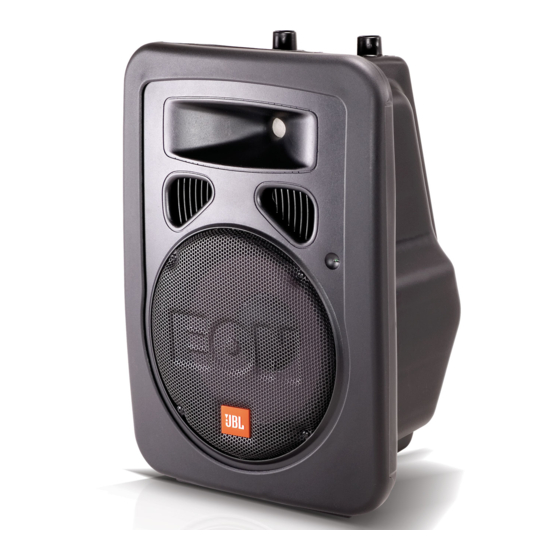
Product Overview The new EON10 G2 compact powered speaker features a 10" woofer, increased power and a three input mini-mixer. The EON10 G2 is ideal for AV applications, smaller musical and spoken word performances and, when combined with the new EONSUB G2 powered subwoofer, provides a full range sound system for small and medium sized events. - Page 4 Specifications Frequency Response Notes: JBL Professional is continually engaged in research activities to enable further product improvement. New materials, production methods and design refinements are instituted into the existing product without notification and, therefore, the information contained within this manual is subject to change without notice.
- Page 5 Connectors...
- Page 6 Indicators...
-
Page 7: Block Diagram
Block Diagram... - Page 8 AC Input PCB The line voltage of 117 Vac is connected at input jack P1 on the ac input PCB. Shunting capacitor C1 reduces the probability of electronic damage that could occur should any abnormalities exist on the input voltage. Capacitors C2 and C3 work in conjunction with C1 to help stabilize this input voltage and reduce the instantaneous line voltage spikes that could cause noise especially in the high frequency range.
- Page 9 Power Supply This is the power supply circuit of the EON 10-G2. Operational voltages, necessary of the main amplifier and processing circuits, are created on this PCB. The schematic, shown above, contains three individual circuits: the signal shutdown, the main rectification and low voltage power supply circuits.
- Page 10 Signal Input Circuitry The above is the XLR line input circuitry for the EON 10-G2. The balanced signal from pins 2,3 of J2 is attenuated by R40 and R39. Signal overload is contained by the signal- limiting diodes, D4 and D1, preventing possible internal IC damage by clamping them to the ±15 Vdc supplies.
- Page 11 Tip Ring Sleeve Input Circuitry Above is the Tip Ring Sleeve jack input circuitry. The input signals are attenuated by R33 and R46 before reaching isolation IC U5A. Multi-path feedback is used to decrease the distortion and increase the stability of the amplifier. The output signal on pin 1 of U5 connects to pin 5 of connector RC1 where volume control, VR2, (not shown) can control the amplitude delivered to loop/mix summing amplifier, U5B (not shown).
- Page 12 Loop/Mix Input Circuitry The loop/mix circuitry, shown above, is another feature that makes the EON 10-G2 so versatile. The user can decide which signal is output to extension male XLR jack J1. SW1 switches between the XLR input signal only or a mixture of the Tip Ring Sleeve and the XLR input signals for increased sound reinforcement.
- Page 13 HF Processing The EON 10G2 utilizes bi-amplification topology to actively filter and separate the high frequency signal from the low frequency signal. Consequently, the low frequency processing circuits are similar. These frequency separation characteristics allow usage of independent, dedicated components for accurate signal reproduction. In the above circuit, the low frequency component of the input signal is effectively attenuated by the 3-pole Butterworth filters consisting of U8B and U8A while the high frequency signal is enhanced.
- Page 14 HF Amplifier Stage After the increase in signal level from U7 pin 1 to 1.1Vpp, the signal enters the monolithic power amplifier IC, U3, at pin 10 via R18, C20 and R11. R12/C23 at the inputs avoid the possibility of phase distortion in the rated 50 Watt output and effectively makes use of common mode rejection to eliminate any induced noise within the audio range.
- Page 15 LF Processing The input signal of magnitude of .49Vpp from P1 at pin 1 from the input/output PCB enters the first stage of the low frequency filtering circuits at R34. The two pole Butterworth filter is used as the active filter configuration due to its flat frequency response. Unity gain to prevent signal distortion with concise filtration characteristics begins at about the 3 kHz cutoff frequency at a rate of -60dB/decade.
- Page 16 LF Amplifier Stage This is the low frequency amplifier. The bridged mode configuration using two LM3886T monolithic amplifiers, U1 and U2, enable twice the output voltage capability than if one IC were driven alone. Therefore, it is strongly recommended this unit be connected to the ac mains through an isolation transformer for safety purposes during the servicing of the amplifier/ output stage.
- Page 17 Peak/Signal Indicator Signal indication is performed by the above circuitry with the possibility of three scenarios-- -normal ac signal present, no signal present and peak signal present. Circuitwise, the high frequency and low frequency output taps are connected to D3 and D4 through R39 /R40 causing reverse charging of capacitor C55.
-
Page 18: Circuit Descriptions
EON10-G2 Troubleshooting Guide The purpose of this troubleshooting guide is to enable the experienced service technician to quickly become familiar with the operating characteristics of the unit and to accurately diagnose the associated symptoms of malfunctioning circuitry to their root causes. - Page 19 Troubleshooting The EON 10-G2 Excessive current draw problems (shorted component) Shorted output IC’s U1, U2, U3 Shorted Power supply components C62, C63, BR1, Q3, Q4, D5 and D6 XFRMR primary/secondary shorted together No voltage/missing voltage/low voltage problems (open/shorted component) Verify proper a.c. input voltage. If all internal voltages are absent, Check that fuses F3 and F4 are ok? Should be 2.5amp 2AG.
- Page 20 If mute pin 8 reads near 0 volts, change IC. If mute pin 8 of any/all output IC’s reads close to –15 volts, recheck above results and signal trace PCB. If the unit measures positive or close to zero the unit is detecting a fault or there exists a problem with the fault detection circuitry.
-
Page 21: Semiconductor Diagrams
Semiconductors Diagrams... -
Page 22: Final Test Procedure
EON10-G2 Final Test Procedure INITIAL POWER UP TEST Setup—Serially connect a variac, isolation transformer and ammeter. Connect unit under test to variac. Mic /Line switch should be Line position. Volume control at fully CCW position and no load. • Slowly increase the variac output voltage monitoring for excessive current usage •... - Page 23 EON10-G2 Pictorial Of Complete Amplifier Assembly Component Parts List Item Part No. Description EON10-G2LF Baf/Cone Assy 125-10000-00X Driver High Freq 271-00002-00 Signal Input Assy 251-00002-00 Main Amp Board Assy 562-00041-00 Transformer 250-00002-00 AC Power Assy...
- Page 24 EON10G2 Pictorial Of Power Input PCB Assembly Component Parts List Item Part No. Description Ref.Des 44-0004 Switch Power 32-1244 Con Plug AC Receptacle 3 Pin 62-0049 Cap 1000 pf Cer 250 V 20% C2,C3 62-0048 Cap 0.01 Mf Cer 250V 20% 32-3189 Fuse 2.5A Time Lag AV 2AG F3,F4...
- Page 25 EON10G2 Pictorial Of Input PCB Assembly Component Parts List Item Part No. Qty. Description Ref.Des. Item Part No. Qty. Description Ref.Des. 72-1480 IC NJM 4580 SM U1,U4,U5 70-1911 LED Multi-color Red/Grn 72-1439 IC 5532 SM 44-0051 Switch 4 PDT , 12 Pin E switch 72-1450 IC TL074 SM 70-1902...
- Page 26 EON10G2 Pictorial Of Main Amplifier PCB Assembly Component Parts List Item Part No. Qty. Description Ref.Des. Item Part No. Qty. Description Ref.Des. 72-0015 IC LM 3886T U3,U1,U2 70-0037 XSTR 2SA1370 PNP 50-0057 Res 10 Ohm 5% SM R1,R2,R23 60-0003 Cap 5600 MF 50V 20% C62,C63 72-0148 IC NJM 4580...
- Page 27 Click here to view the JBL Limited Warranty Statement http://www.jblpro.com/pub/technote/warranty.pdf Click here for the Systems Exploded View / Mechanical Assembly Drawings http://www.jblproservice.com/pdf/EON-G2%20Series/EON10G2.pdf Click here to view the JBL Professional QA Codes http://www.jblproservice.com/protected/Domestic%20pdf/Electronic%20QA%20Codes.pdf http://www.jblproservice.com/protected/Domestic%20pdf/Loudspeakers%20and%20Loudspeaker%20System%20QA%20Codes.pdf Click here for the Main Board Schematics http://www.jblproservice.com/pdf/EON-G2%20Series/EON10-G2%20Main%20Amp%20Schematics.pdf Click here for the Main Board Parts List http://www.jblproservice.com/pdf/EON-G2%20Series/EON10-G2%20Main%20Amp%20Parts%20List.pdf...
- Page 29 JBL Incorporated, 8500 Balboa Boulevard, P.O. Box 2200, Northridge, California 91329 U.S.A. Technical Manual JBL EON10-G2 SPECIFICATIONS ACOUSTIC & ELECTRICAL SPECIFICATIONS: SYSTEM COMPONENTS: (CONT’D) • Amplifier Power LF: 125 Watts @ Low Frequency • Input 1 Sensitivity: -48 dBu to 0 dBu for Rated Output Driver Impedance.
- Page 30 JBL EON10-G2 Tie Wrap 925-00001-00 Transformer Amplifier PCA WHITE F .110 — H.F. (24112) BLUE F .205 + LED Assembly Ground Wires Screw to be Located 864-41600-08 BLACK Between Baffle TF, PPH, F .187 — Boss and LED 10-32 x 1/2 PAN, PDB, Secure L.F.
- Page 31 JBL EON10-G2 Screw (14) Rear Enclosure AC Power Assy 900401-016 380-90021-00 250-00002-00 MS, PPH, Eon10-G2 EON10-G2 10-32 x 1 BLK BAF/Cone Assy Rivet, Plastic Label EON10-G2LF 869-90000-05 337501-003 120V, EONG2 Bezel 382-00380-01 Screw (12) Label EON10-G2 864-41600-06 337501-005 TF, PPH,...
- Page 32 JBL EON10-G2 COMPONENT EXPLODED VIEW Label 480-00100-00 120V EON10-G2 Label 480-00100-01 230V, EON10-G2/230 Screw (4) 864-41600-08 10-32 x 1/2 PAN, PH, TT, CLR, ZINC Driver, High Freq 2412H use 125-10000- Nut Retainer Tinn U-Type 330652-001 Washer, Transformer Mounting 885-00088-00 Transformer...
- Page 33 JBL PROFESSIONAL SERVICE PROCEDURES July 1, 1998 ELECTRONIC FAILURE CODES The following codes are an expanded version of the existing electronic failure codes. These codes should be used for all electronics excluding networks in speaker enclosures. Network failures should continue to use the transducer failure codes. Please utilize these codes on every warranty claim submitted to JBL Professional.
- Page 34 JBL PROFESSIONAL ELECTRONIC FAILURE Q.A. CODES July 1, 2004 Page 1 Q.A. DESCRIPTION OF DEFECT WARRANTY Q.A. DESCRIPTION OF DEFECT WARRANTY CODE STATUS CODE STATUS 10.052 Capacitor - Burned due to Workmanship/Design 10.010 IC (Specify) 10.011 IC - Open 10.053 Capacitor - Shorted 10.012 IC - Burned due to Workmanship/Design 10.054 Capacitor - Thermally Sensitive 10.013 IC - Shorted...
- Page 35 JBL PROFESSIONAL ELECTRONIC FAILURE Q.A. CODES July 1, 2004 Page 2 Q.A. DESCRIPTION OF DEFECT WARRANTY Q.A. DESCRIPTION OF DEFECT WARRANTY CODE STATUS CODE STATUS 10.113 Switch - Will Not Close 10.172 Transformer - Burned due to Workmanship/Design 10.114 Switch - Noisy 10.173 Transformer - Noisy 10.175 Transformer - Shorted 10.120 FUSE (Specify)
- Page 36 JBL PROFESSIONAL ELECTRONIC FAILURE Q.A. CODES July 1, 2004 Page 3 Q.A. DESCRIPTION OF DEFECT WARRANTY Q.A. DESCRIPTION OF DEFECT WARRANTY CODE STATUS CODE STATUS 10.602 Adjust Bias 10.603 Adjust Meter 10.604 Adjust Chassis 10.700 MISC/HARDWARE (Specify) 10.701 Screw - Missing (from factory) 10.702 Screw - Broken (from factory) 10.703 Screw - Loose (from factory) 10.704 No Problems Found...
- Page 37 JBL PROFESSIONAL LOUDSPEAKERS AND LOUDSPEAKER SYSTEM Q.A. CODES July 1, 2004 Page 1 Q.A. DESCRIPTION OF DEFECT WARRANTY Q.A. DESCRIPTION OF DEFECT WARRANTY CODE STATUS CODE STATUS No Defects - Definition 3.11 Open – Break at Eyelet No Defects - Unclassified 3.12 Open - Solder Joint at Eyelet No Defects - Standard...
- Page 38 JBL PROFESSIONAL LOUDSPEAKERS AND LOUDSPEAKER SYSTEM Q.A. CODES July 1, 2004 Page 2 Q.A. DESCRIPTION OF DEFECT WARRANTY Q.A. DESCRIPTION OF DEFECT WARRANTY CODE STATUS CODE STATUS External Damage to the frame resulting in Horn failures – (Specify) distortion of its structural members External Damage - Magnet Assembly Appearance - Color or Scratches –...
- Page 39 056393b0.sch-1 - Tue Jun 19 14:05:14 2001...
- Page 40 056393b0.sch-2 - Tue Jun 19 14:06:23 2001...
- Page 41 056393b0.sch-3 - Tue Jun 19 14:06:31 2001...
- Page 42 056393b0.sch-4 - Tue Jun 19 14:05:49 2001...
- Page 43 056393b0.sch-5 - Tue Jun 19 14:05:58 2001...
- Page 44 056393b0.sch-6 - Tue Jun 19 14:06:41 2001...
- Page 45 056393b0.PPS Bill Of Materials for 056393b0.sch on Tue Jun 19 14:03:50 2001 ------------------------------------------------------------------------------------------------------------------------------------------------------- Reference HMG# Description Audit Schematic Part PCB Decal ------------------------------------------------------------------------------------------------------------------------------------------------------- PCB1 80-6393 PCB 80-6393 EON10 GII Main Board PT2044 80XXXXYY BARCODE 70-0094 DIO BRGE RECT 200V 10A BK PT2308 BR700094 BRIDGE4 A1-41...
- Page 46 056393b0.PPS R13 R15 52-3242 RES 280K 1% 1/10W SM 0805 TA PT1696 R280KC1-0805 0805 52-4506 RES 2K 1% 1/10W SM 0805 TA PT1038 R2KC1-0805 0805 R3 R5 R7 R9 52-3220 RES 30.1K 1% 1/10W SM 0805 TA PT1721 R30.1KC1-0805 0805 52-4492 RES 36.5K 1% 1/10W SM 0805 TA PT2160 R36.5KC1-0805...
- Page 47 056392a1.sch-2 - Mon Feb 05 17:13:31 2001...
- Page 48 056391A0.SCH-1 - Mon Nov 13 11:02:25 2000...
- Page 49 056392a1.PPS Bill Of Materials for 056392a1.sch on Mon Feb 05 17:09:00 2001 ------------------------------------------------------------------------------------------------------------------------------------------------------- Reference HMG# Description Audit Schematic Part PCB Decal ------------------------------------------------------------------------------------------------------------------------------------------------------- PCB1 80-6392 PCB 80-6392 JBL EON AC INPUT PCB PT2044 80XXXXYY BARCODE 10-6392 BKT JBL EON10 GII INPUT POWER P&S PT2336 BK106392 PCBNULL 14-6392...
- Page 50 056391A0.SCH-2 - Mon Nov 13 11:02:46 2000...
- Page 51 056391A0.SCH-3 - Mon Nov 13 11:03:04 2000...
- Page 52 056391a0.pps Bill Of Materials for 056391A0.SCH on Mon Nov 13 11:01:02 2000 ------------------------------------------------------------------------------------------------------------------------------------------------------- Reference HMG# Description Audit Schematic Part PCB Decal ------------------------------------------------------------------------------------------------------------------------------------------------------- PCB1 80-6391 PCB 80-6391 EON10 SIGNAL BOARD PT2044 80XXXXYY BARCODE NON-PART NON-PART, PCB ONLY, BREAKOFF PART PT1481 BRKOFF BRKOFF C16-17 C21 56-0003...
- Page 53 JBL PROFESSIONAL CUSTOMER SERVICE DEPARTMENT EON-G2 SERIES REFERENCE CHART Revision C - February 4, 2004 Page 1 of 2 MODEL LOW FREQ. HIGH MAIN AC POWER SIGNAL INPUT LAST REPAIR KIT FREQUENCY AMP PCBA INPUT PCBA PCBA YR MFD EON10-G2 C8REON10-G2 2412H (125-10000-00X 251-00002-00 250-00002-00 350316-001...
- Page 54 JBL PROFESSIONAL CUSTOMER SERVICE DEPARTMENT EON-G2 SERIES REFERENCE CHART Revision C - February 4, 2004 Page 2 of 2 MODEL EON15-G2 SYS - Fully Integrated Professsional Sound System, includes 2 EON15-G2 Two-Way Powered Speakers, the MusicMix 16 sound reinforcement Mixer, Two M50S Dynamic Microphones, and all necessary cabling. EON10-G2 SYS - Fully Integrated Professsional Sound System, includes 2 EON10-G2 Two-Way Powered Speakers, the MusicMix 14 sound reinforcement Mixer, Two M50S Dynamic Microphones, and all necessary cabling.
Need help?
Do you have a question about the JBL EON10-G2 and is the answer not in the manual?
Questions and answers