Table of Contents
Advertisement
Quick Links
Please file and use this service manual together with the service manual for CR14D, Order No.
PSG0905054AE
TABLE OF CONTENTS
1 Safety Precautions----------------------------------------------- 3
1.1. GENERAL GUIDELINES -------------------------------- 3
1.2. Before Repair and Adjustment ------------------------- 3
1.3. Protection Circuitry ---------------------------------------- 3
1.4. Safety Parts Information --------------------------------- 4
2 Warning -------------------------------------------------------------- 5
to Electrostatic Sensitive (ES) Devices -------------- 5
2.2. Precaution of Laser Diode------------------------------- 6
Model No.
Product Color: (K)...Black Type
PAGE
2.4. Handling Precautions for Traverse Unit --------------8
3 Service Navigation --------------------------------------------- 10
3.1. Service Information -------------------------------------- 10
4 Specifications ---------------------------------------------------- 11
5 Location of Controls and Components------------------ 13
5.1. Main Unit Key Button Operation---------------------- 13
5.2. Remote Control Key Button Operation ------------- 14
5.3. Disc Information ------------------------------------------ 15
5.4. Using the Music Port ------------------------------------ 17
5.5. DivX VOD Content--------------------------------------- 18
© Panasonic Corporation 2009. All rights reserved.
Unauthorized copying and distribution is a violation
of law.
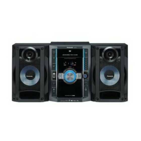
DVD Stereo System
SA-VK480EE
PSG0906001CE
PAGE
Advertisement
Table of Contents
Troubleshooting

Related Manuals for Panasonic SA-VK480EE


Summary of Contents for Panasonic SA-VK480EE
-
Page 1: Table Of Contents
2.2. Precaution of Laser Diode------------------------------- 6 5.4. Using the Music Port ------------------------------------ 17 2.3. Service caution based on Legal restrictions -------- 7 5.5. DivX VOD Content--------------------------------------- 18 © Panasonic Corporation 2009. All rights reserved. Unauthorized copying and distribution is a violation of law. - Page 2 5.6. USB - Play and Recording ----------------------------- 19 12.2. Tape Speed Adjustment-------------------------------- 90 6 Self-Diagnosis and Special Mode Setting -------------- 21 12.3. Bias Voltage Check ------------------------------------- 91 6.1. Service Mode Summary Table ------------------------ 21 12.4. Bias Frequency Check -------------------------------- 91 6.2.
-
Page 3: Safety Precautions
1 Safety Precautions 1.1. GENERAL GUIDELINES 1. When servicing, observe the original lead dress. If a short circuit is found, replace all parts which have been overheated or damaged by the short circuit. 2. After servicing, see to it that all the protective devices such as insulation barriers, insulation papers shields are properly installed. -
Page 4: Safety Parts Information
“shorted”, or if speaker systems with an impedance less than the indicated rated impedance of the amplifier are used. If this occurs, follow the procedure outlines below: 1. Turn off the power. 2. Determine the cause of the problem and correct it. 3. -
Page 5: Warning
2 Warning 2.1. Prevention of Electrostatic Discharge (ESD) to Electrostatic Sensitive (ES) Devices Some semiconductor (solid state) devices can be damaged easily by static electricity. Such components commonly are called Elec- trostatically Sensitive (ES) Devices. Examples of typical ES devices are integrated circuits and some field-effect transistors and semiconductor "chip"... -
Page 6: Precaution Of Laser Diode
2.2. Precaution of Laser Diode Caution: This product utilizes a laser diode with the unit turned “on”, invisible laser radiation is emitted from the pickup lens. Wavelength: 655nm (DVD) / 785 nm (CD) Maximum output radiation power from pickup: 100 µW/VDE Laser radiation from the pickup unit is safety level, but be sure the followings: 1. -
Page 7: Service Caution Based On Legal Restrictions
2.3. Service caution based on Legal restrictions 2.3.1. General description about Lead Free Solder (PbF) The lead free solder has been used in the mounting process of all electrical components on the printed circuit boards used for this equipment in considering the globally environmental conservation. The normal solder is the alloy of tin (Sn) and lead (Pb). -
Page 8: Handling Precautions For Traverse Unit
2.4. Handling Precautions for Traverse Unit The laser diode in the optical pickup unit may break down due to static electricity of clothes or human body. Special care must be taken avoid caution to electrostatic breakdown when servicing and handling the laser diode in the traverse unit. Cautions to Be Taken in Handling the Optical Pickup Unit 2.4.1. - Page 9 2.4.2.2. Human body grounding 1. Use the anti-static wrist strap to discharge the static electricity form your body. Figure 2...
-
Page 10: Service Navigation
3 Service Navigation 3.1. Service Information This service manual contains technical information which will allow service personnel’s to understand and service this model. Please place orders using the parts list and not the drawing reference numbers. If the circuit is changed or modified, this information will be followed by supplement service manual to be filed with original service manual. -
Page 11: Specifications
0.7 mV, 1.2 kΩ pictures may not be displayed. Terminal Mono, 6.3 mm jack (1 system) MPEG4 data recorded with the Panasonic SD multi cameras or DVD video recorders. Conforming to SD VIDEO specifications (ASF Terminal RCA jack standard)/ MPEG4 (Simple Profile) video system/ G.726 audio system. -
Page 13: Location Of Controls And Components
5 Location of Controls and Components 5.1. Main Unit Key Button Operation AC supply indicator (AC IN) This indicator lights when the unit is connected to Remote control signal sensor the AC mains supply. Standby/on switch ( Press to switch the unit from on to standby mode Disc trays or vice versa. -
Page 14: Remote Control Key Button Operation
Remote Control Key Button Operation TV operations Turn the unit on/off (Aim the remote control to a Panasonic TV and press the button. Show disc information/Select a disc Only works with some models) [ ]: turn the TV on/off Play loaded discs in order... -
Page 15: Disc Information
Recorded using a format different from DVD-Video Format, therefore, some functions cannot be used. MPEG4 data recorded with the Panasonic SD multi cameras or DVD video recorders [conforming to SD VIDEO specifications (ASF standard)/MPEG4 (Simple Profile) video system/G.726 audio system]. - Page 16 Keep the number specifications (ASF standard)/MPEG4 (Simple Profile) video of sessions to a minimum to avoid this. system/G.726 audio system] recorded with Panasonic SD Naming folders and files Example: multi cameras or DVD video recorders with this unit.
-
Page 17: Using The Music Port
5.4. Using the Music Port You can playback sound from portable audio equipment. Sound from the speaker may be distorted if the portable audio equipment s equalizer (if any) is turned on. Turn it off before you plug into the MUSIC PORT jack. Preparation Reduce the volume of the unit and portable audio equipment before connecting or disconnecting. -
Page 18: Divx Vod Content
5.5. DivX VOD Content This DivX Certified device must be registered in order to play DivX Video-on-Demand (VOD) content. First generate the DivX VOD registration code for your device and submit it during the registration process. [Important: DivX VOD content is protected by a DivX DRM (Digital Rights Management) system that restricts playback to registered DivX Certified devices. If you try to play DivX VOD content not authorized for your device, the message Authorization Error will be displayed and your content will not play.] Learn more at www.divx.com/vod. -
Page 19: Usb - Play And Recording
It may not be possible to play all the files due to the condition Note on how they were created. MP3 file needs to be selected before recording can begin. All For Panasonic D-Snap/DIGA files in the current folder will be recorded. Non-MP3 files will be skipped. Note Files in subfolder will be ignored. - Page 20 Recording from audio disc (CDDA) Track Divide This function allows you to divide between tracks. You can Connect the USB mass storage device choose; Insert the disc(s) you want to record. AUTO 5M, track is automatically divided every 5 minutes. Press [DVD/CD ] and then [ ] twice.
-
Page 21: Self-Diagnosis And Special Mode Setting
6 Self-Diagnosis and Special Mode Setting This unit is equipped with features od self-diagnosis & special mode setting for checking the function & reliability. Special Note: Checking of the reliability (ageing) & changer operation must be carry out to ensure good working condition in unit. - Page 22 Note: An error code will be canceled if a power supply is turned OFF. *1: CPPM is the copy guard function beforehand written in the disk for protection of copyrights. *2: CEC is the consumer electronic control used for high-level user control of HDMI-connected devices. *3: HDCP is the specification developed to control digital audio &...
-
Page 23: Doctor Mode Table
6.2. Doctor Mode Table Item Key Operation FL Display Mode Name Description Front Key (Display 1) Doctor Mode To enter into Doctor Mode for checking In CD Mode: of variuos items and displaying 1. Press [ ] button -DEMO EEPROM and firmware version. on main unit follow by [4] and [7] on remote control. -
Page 24: Self-Diagnosis Mode Table
6.3. Self-Diagnosis Mode Table 6.3.1. Self-Diagnosis Mode Table 1 Item Key Operation FL Display Mode Name Description Front Key Self-Diagnostic To enter into self-diagnostic checking In DVD/CD mode (ensure no disc is Mode for CR14D mechanism. inserted): Press and hold [STOP] button for five seconds, followed by [ /FF/ button on the main unit. -
Page 25: Service Mode Table (For Dvd)
6.3.2. Self-Diagnosis Mode Table 2 Item Key Operation FL Display Mode Name Description Front Key Reliability To determine playability operation. Display 1 In self-diagnostic mode, press [2] button on remote control. (Traverse Cycle Test) To exit, press [ ] button on the main unit or remote control unit. - Page 26 6.4.1. Service Mode Table 1 Item Key Operation FL Display Mode Name Description Front Key Jitter check Jitter check. In STOP (no disc) mode, (Display 1) Jitter rate is measured and displayed. press [STOP] button on the Measurement is repeatedly done in main unit, and [5] button on the cycle of one second.
- Page 27 6.4.2. Service Mode Table 2 Key Operation Item FL Display Mode Name Description Front Key (Display 1) DVD laser DVD laser drive current measurement. In STOP (no disc) mode, drive current DVD laser drive current is measured press [STOP] button on the measurement and the result is displayed together main unit, and...
- Page 28 6.4.3. Service Mode Table 3 Item Key Operation FL Display Mode Name Description Front Key Micro-processor Micro-processor firmware version In STOP (no disc) (Display 1) firmware version display & EEPROM checksum display. mode, press [STOP] display & EEPROM checksum is only available button on the main unit, EEPROM due to existence of EEPROM IC.
- Page 29 Product TV Broadcasting Region Model Series Country Region Signal System Region Display OSD Menu Language Code System Default (Default) (Default) English, Spanish, English P, PC, PX USA, Canada, PX NTSC NTSC (*A) Canadian, French Japanese Japan NTSC NTSC (*A) Japanese, English English, French, German, English Europe...
- Page 30 6.4.4. Service Mode Table 4 Item Key Operation FL Display Mode Name Description Front Key DVD Module DVD Module P.C.B. firmware version In STOP (no disc) P.C.B. firmware is displayed on the FL Display. mode, press [STOP] version display The firmware version can be updated button on the main unit, using recovery disc.
- Page 31 6.4.5. Service Mode Table 5 Item Key Operation FL Display Mode Name Description Front Key Timer 1 check Timer 1 check In STOP (no disc) (Display 1) Laser operation timer is measured mode, press [STOP] separately for DVD laser and CD laser. button on the main unit, and [ ] button on the...
- Page 32 6.4.6. Optical Pick-up Self-Diagnosis The optical pickup self-diagnosis function and tilt adjustment check function have been included in this unit. When repairing, use the following procedure for effective self-diagnosis and tilt adjustment. Be sure to use the self-diagnosis function before replacing the optical pickup when "NO DISC"...
-
Page 33: Dvd Self Diagnostic Function-Error Code
6.5. DVD Self Diagnostic Function-Error Code 6.5.1. DVD Module Error Code Table Error Diagnosis Contents Description of error Automatic FL Display Remarks Code U702 HDMI/DVI I2C The communication error of I2C when Press [ STOP] on main communication error connecting it with HDMI/DVI. For unit for next error. - Page 34 6.5.2. DVD Mechanism Unit (CR14D) Error Code Table Error Diagnosis Contents Description of error Automatic FL Display Remarks Code H01 Tray loading error The tray opening and closing is Press [ STOP] on abnormal. CLOSE and OPEN of the main unit for next error. tray cannot be carried out properly.
- Page 35 6.5.3. Power Supply & Digital Amplifier Error Code Table Error Diagnosis Contents Description of error Automatic FL Display Remarks Code F61 The abnormalities In normal operation, when DCDET2 goes Press [ STOP] on main in an output or power to "L" (Low) (Not during POWER OFF unit for next error.
- Page 36 6.5.5. DVD Changer Mechanism Unit (CR14D) Error Code Table Error Code Diagnosis Contents Description of error Automatic FL Display Remarks LOAD Load operation faulty The load operation cannot For DVD Mechanism unit (CR14D). complete when time out Press [EXCHANGE] on main unit for occurs.
-
Page 37: Sales Demonstration Lock Function
6.5.6. Deck Mechanism Error Code Table 6.6. Sales Demonstration Lock Function This function prevents discs from being lost when the unit is used for sales demonstrations by disabling the disc eject function. "LOCKED" is displayed on the unit, and ordinary operation is disabled. 6.6.1. -
Page 38: Troubleshooting Guide
7 Troubleshooting Guide 7.1. Troubleshooting Guide for F61 and/or F76 This section illustrates the checking procedures when upon detecting the error of “F61” and/or “F76” after power up of the unit. It is for purpose of troubleshooting and checking in SMPS, D-Amp & Main P.C.B. 7.1.1. - Page 39 7.1.2. Troubleshooting Guide Symptom Checking Items Repair Items Remarks Check the soldering of the SMPS Tou ch-up the solder crack area/ FL display blinking with SMPS P. C.B. Change the defective parts. abnormal segment when P. C.B. Is there any solder crack at area Q5860,Q5861,Q5862,TH5860 power ON the set or "F61"...
- Page 40 7.1.3. Part Location 7.1.3.1. SMPS P.C.B. Feedback circuit: PC5720, D5725 +30V Detect: QR5801, QR5802, Temperature Detect: Q5860, Q5681, Q5862 Temperature Detect: TH5860 Feedback Circuit: IC5801, Q5802, D5806 SMPS P.C.B. Figure 2 SMPS P.C.B.
- Page 41 7.1.3.2. D-Amp P.C.B. Audio Digital Power Amp IC: IC5000 D-Amp P.C.B. Figure 3 D-Amp P.C.B.
- Page 42 7.1.3.3. Main P.C.B. Connector: CN2807 Fuse Protector: FP2091 Switching Regulator IC: IC4000 T2900, D2901 Figure 4 Main P.C.B.
- Page 43 7.1.3.4. D-Amp IC Configuration VK480EE Pin (10) Front Right IC5000 Pin (14) Front Left Figure 5...
-
Page 44: Basic Troubleshooting Guide For Traverse Unit (Dvd Module P.c.b.)
7.2. Basic Troubleshooting Guide for Traverse Unit (DVD Module P.C.B.) Problems Checking Points Checking components 1) Distorted picture or a) Check SDRAM address, data IC8051 abnormal sound is head bus, CLK and other control signals during the initialization waveform b) Check video signals (Y,C) LB8301, R8321, R8323, LB8302, R8325, R8327 c) Check audio DAC circuitry... -
Page 45: Service Fixture & Tools
8 Service Fixture & Tools 8.1. Service Tools and Equipment Prepare service tools before process service position. Service Tools Remarks Main P.C.B. (CN2808) - D-Amp P.C.B. (CN5050) REEX0930 (17P FFC) Main P.C.B. (ZJ2701) - SMPS P.C.B. (CN5802) REXX0680 (11P Cable) SMPS P.C.B. -
Page 46: Disassembly And Assembly Instructions
9 Disassembly and Assembly Instructions “ATTENTION SERVICER” Be careful when disassembling and servicing. Some chassis components may have sharp edges. Special Note: 1. This section describes the disassembly procedures for all the major printed circuit boards and main components. 2. Before the disassembly process was carried out, do take special note that all safety precautions are to be carried out. -
Page 48: Disassembly Flow Chart
9.1. Disassembly flow chart The following chart is the procedure for disassembling the casing and inside parts for internal inspection when carrying out the ser- vicing. To assemble the unit, reverse the steps shown in the chart as below. 9.3 Top Cabinet 9.4 DVD Mechanism 9.7 Front Panel Assembly 9.19 D-Amp P.C.B. -
Page 49: Main Components And P.c.b. Location
9.2. Main Components and P.C.B. Location... -
Page 50: Disassembly Of Top Cabinet
9.3. Disassembly of Top Cabinet Step 1 Remove 3 screws on each side of the main unit. Step 3 Lift the sides of top cabinet outwards as arrow shown. Step 2 Remove 5 screws. Step 4 Push the top cabinet backwards as arrow shown to release the catches. -
Page 51: Disassembly Of Dvd Mechanism Unit (Cr14D)
Step 5 Remove the top cabinet. Step 2 Detach 50P FFC cable at the connector (CN2801) on Main P.C.B. 9.4. Disassembly of DVD Mecha- Step 3 Detach 11P FFC cable at the connector (CN2805) on nism Unit (CR14D) Main P.C.B. Step 4 Detach 5P cable at the connector (CN1113) on USB •... - Page 52 Caution: During assembling, ensure the claws are fully catched. Caution: During assembling, ensure that the DVD Mecha- nism Unit (CR14D) is seated properly at the locator. Step 6 Release the DVD Mechanism Unit (CR14D) from the catches and locators. Step 7 Lift up DVD Mechanism Unit (CR14D) in the direction of arrow.
-
Page 53: Disassembly Of Dvd Module P.c.b
Step 10 Remove 7P FFC from the Ferrite Core. Caution: Ensure that 7P FFC is properly slot through the Step 1 Remove 3 screws. Ferrite Core. Step 2 Remove the shield plate unit. Step 3 Remove DVD Module P.C.B.. 9.6. Disassembly of Rear Panel •... -
Page 54: Disassembly Of Front Panel Assembly
Step 1 Detach 27P FFC at the connector (CN2807) on Main P.C.B.. Step 2 Detach 2P cable at the connector (CN2813) on Main P.C.B.. Step 3 Detach 5P cable at the connector (CN1113) on USB P.C.B.. Step 3 Slightly lift up the DVD Mechanism Unit (CR14D) to release from the two locators. -
Page 55: Disassembly Of Mic P.c.b
Caution: Do not exert strong force when releasing the tabs. Step 8 Release the claws on both sides. Step 9 Release catches at both side. Caution: During assembling, ensure that both claws and catches are fully catched. Step 11 Remove 1 screw to remove ground wire. Step 12 Remove front panel assembly in the direction of arrow. -
Page 56: Disassembly Of Panel P.c.b., Volume P.c.b
Step 2 Detach 7P cable at the connector (CN6702) on Mic P.C.B.. Step 2 Detach 7P cable at the connector (CN6702) on Mic P.C.B.. Step 3 Remove 1 screw on Mic P.C.B.. Step 4 Remove the Mic P.C.B.. 9.9. Disassembly of Panel P.C.B., Volume P.C.B. - Page 57 Step 4 Remove 2 screws on Volume P.C.B.. Step 6 Release 6 catches at Volume P.C.B.. Step 7 Release 2 catches at Remote Sensor P.C.B.. Step 5 Release 2 catches at Panel P.C.B..
-
Page 58: Disassembly Of Usb P.c.b
Caution: During assembling, ensure that the diodes shown on Volume P.C.B. are in upright position. Step 8 Lift up the Panel P.C.B., Volume P.C.B. & Remote Sen- sor P.C.B. altogether as arrow shown. • Disassembly of Side Bar (L) Led P.C.B. and Side Bar (R) P.C.B. -
Page 59: Disassembly Of Music Port P.c.b
• Disassembly of USB Jack holder. Step 1 Remove 2 screws at USB Jack holder. Step 1 Remove 2 screws at Music Port P.C.B.. Step 2 Remove the USB Jack Holder together with USB Step 2 Release 2 catches. P.C.B.. Step 3 Lift up to remove Music Port P.C.B.. -
Page 60: Disassembly Of Deck Mechanism Unit
Caution: During assembling, please ensure that the spring is assembly at right position. Step 2 Remove CD Lid as arrow shown. 9.13. Disassembly of Deck Mecha- nism Unit • Follow the (Step 1) to (Step 5) of Item 9.3 • Follow the (Step 1) to (Step 12) of Item 9.7 Step 2 Push the lever upward as arrow shown to open the cas- sette lid. -
Page 61: Disassembly Of Deck P.c.b
9.14. Disassembly of Deck P.C.B. • Follow the (Step 1) to (Step 5) of Item 9.3 • Follow the (Step 1) to (Step 12) of Item 9.7 • Follow the (Step 1) to (Step 3) of Item 9.13 Step 1 Remove 2 screws. Step 2 Remove shield plate. -
Page 62: Disassembly Of Deck Mechanism
Step 1 Desolder the plunger terminals. Step 4 Remove Deck Mechanism P.C.B.. Step 2 Remove 1 screw. Caution: During assembling, ensure that the Deck Mecha- nism P.C.B. is seated properly with the guide of the loca- tors. Step 3 Release 4 catches. 9.16. - Page 63 • Follow the (Step 1) to (Step 12) of Item 9.7 Caution: Avoid exerting strong force as it may damage the FFC. • Follow the (Step 1) to (Step 3) of Item 9.13 • Follow the (Step 1) to (Step 4) of Item 9.15 9.16.1.
- Page 64 9.16.2. Replacement of Capstan Motor Ass’y and Capstan Belt ‘A’ • Follow the (Step 3) to (Step 4) of item 9.16.1. - Disassembly of Capstan Motor Ass’y and Capstan Belt ‘A’ Step 2 Lift up to remove the Sub-Chassis Ass’y. Step 1 Remove 3 screws.
- Page 65 Step 4 Remove Capstan Belt ‘A’. - Assembly of Capstan Motor Ass’y and Capstan Belt ‘A’ Step 1 Coil Capstan Belt ‘A’ to Flywheel ‘F’ Ass’y, Flywheel ‘L’ and the 2 bosses temporarily as diagram shown. Caution: Keep Capstan Belt ‘A’ away from grease during assembly of Capstan Belt ‘A’.
- Page 66 Step 2 Fit the Capstan Motor Ass’y to the Sub-Chassis Ass’y. Caution: Ensure it seats properly. Step 3 Fix the Capstan Motor Ass’y to the Sub-Chassis Ass’y by 2 screws. Step 5 Fix 3 screws. Step 6 Release Capstan Belt ‘A’ to the pulley of Capstan Motor Ass’y as diagram shown.
- Page 67 Step 1 Release 2 catches and press the tip of the Winding Lever downwards. Step 2 Remove Flywheel ‘L’ Ass’y. Step 3 Remove the Winding Lever. Step 4 Remove the Thrust Spring. Step 5 Remove the Winding Arm Ass’y. Step 6 Remove the Flywheel ‘F’ Ass’y. Step 7 Remove the Winding Belt.
- Page 68 Step 3 Install Flywheel ‘F’ Ass’y. Step 1 Install the Winding Arm Ass’y. Caution: Ensure that the boss and the marking hole of the Main Gear are positioned such that they form a horizontal line parallel to the Deck Mechanism Unit. Step 2 Coil the Winding Belt to the Winding Arm Ass’y and the 2 bosses temporarily as diagram shown.
- Page 69 Step 4 Install the Thrust Spring. Step 5 Install the Winding Lever. Caution 2: Ensure that the Winding Lever is firmly inserted and properly catched on the tape side as diagram shown. Caution 1: Ensure that the Winding Arm Ass’y is pulled towards to the right as arrow shown to enable full insertion of the Winding Lever.
- Page 70 Step 7 Install Flywheel ‘L’ Ass’y. 9.16.4. Disassembly of Main Gear • Follow the (Step 3) to (Step 4) of item 9.16.1. • Follow the (Step 1) to (Step 4) of item 9.16.2. • Follow the (Step 1) to (Step 6) of item 9.16.3. Caution 3: Ensure that the Winding Belt is above the Wind- ing Lever as diagram shown.
-
Page 71: Disassembly Of Cassette Lid
Step 1 Remove the spring. Step 2 Push the cassette lid in the direction of arrows. 9.18. Rectification Tape Problem • Follow the (Step 1) to (Step 5) of Item 9.3 Step 1 Rotate the flywheel F in the direction of the arrow. Caution : Ensure that the boss and the marking hole of the Main Gear are positioned such that they form a horizontal line parallel to the Deck Mechanism during assembly of... - Page 72 • Follow the (Step 1) to (Step 6) of Item 9.4 Step 1 Remove 4 screws at the rear panel. Step 5 Lift up the D-Amp P.C.B. together with the inner chassis assembly as arrow shown. Step 6 Remove 2 screws on D-Amp P.C.B.. Step 2 Detach 17P FFC at the connector (CN5050) on D-Amp P.C.B..
-
Page 73: Replacement Of Audio Digital Power Amp Ic (Ic5000)
Caution: During assembling, ensure the D-Amp P.C.B. is seated properly on the locator of the Inner chassis assem- bly. 9.20. Replacement of Audio Digital Step 3 Remove 1 screw. Power Amp IC (IC5000) Step 4 Remove TR Spring in the direction of arrow shown. Step 5 Remove Audio Digital Power Amp IC (IC5000). -
Page 74: Disassembly Of Main P.c.b
Caution: Ensure pins of the Audio Digital Power Amp IC (IC5000) are properly seated and soldered on D-Amp P.C.B.. 9.21. Disassembly of Main P.C.B. • Follow the (Step 1) to (Step 5) of Item 9.3 • Follow the (Step 1) to (Step 7) of Item 9.4 •... -
Page 75: Replacement Of Switching Regulator Ic (Ic5701)
Step 4 Flip the SMPS P.C.B. and desolder 2 wires pins (red and black). Step 1 Detach 11P cable at the connector (CN5802) on SMPS P.C.B.. Caution: During assembling, ensure that SMPS P.C.B. is seated properly at the locators. 9.23. Replacement of Switching Reg- ulator IC (IC5701) •... -
Page 76: Replacement Of Rectifier Diode (D5702)
Step 1 Apply grease to the Heatsink Unit B. Step 2 Mount the Switching Regulator IC (IC5701) on to SMPS P.C.B.. Caution: Ensure pins of the switching regulator IC (IC5701) are properly seated on SMPS P.C.B. Step 1 Desolder pins of the switching regulator IC (IC5701) on the solder side of SMPS P.C.B. - Page 77 Caution: During replacement of the part, avoid touching the heatsink, it may lead to injuries. 9.24.2. Assembly of Rectifier Diode (D5702) Step 1 Desolder pins of the Rectifier Diode (D5702) on the sol- Step 1 Apply grease to the Heatsink Unit B. der side of SMPS P.C.B..
-
Page 78: Replacement Of Regulator Diode (D5801)
Step 6 Solder pins of the Heatsink Unit B on the solder side of Caution: During replacement of the part, avoid touching SMPS P.C.B.. the heatsink, it may lead to injuries. 9.25.2. Assembly of Regulator Diode 9.25. Replacement of Regulator (D5801) Diode (D5801) •... -
Page 79: Replacement Of Regulator Diode (D5803)
Caution: Ensure the Regulator Diode (D5802) is well tight- ened to the heatsink unit C. Step 1 Desolder pins of the Regulator Diode (D5802) on the solder side of SMPS P.C.B.. Step 3 Solder pins of the Regulator Diode (D5802) on the sol- der side of SMPS P.C.B.. -
Page 80: Disassembly Of Ac Inlet P.c.b
Caution: Ensure pins of the regulator diode (D5803) are properly seated and soldered on SMPS P.C.B.. 9.28. Disassembly of AC Inlet P.C.B. • Follow the (Step 1) to (Step 5) of Item 9.3 Step 2 Remove 1 screw. Step 3 Remove the Regulator Diode (D5803) from the Heatsink Unit C. - Page 81 Step 4 Detach the rear panel slightly backward as arrow shown. Step 5 Lift up the AC Inlet P.C.B.. Step 6 Flip over the AC Inlet P.C.B. and desolder AC Inlet wires (red and black). Caution: During assembling, ensure the P.C.B. is seated properly at the locators.
-
Page 82: Disassembling And Assembling Of Traverse Unit
10 Disassembling Step 1 Release the catch and push the guide as arrows shown to open both grooves. Assembling of Traverse Unit Note: Refer to Section 6.3.1. Self-Diagnosis Mode Table 1 to set to Service Mode 2. 10.1. Disassembly Procedures Step 2 Detach the FFC wires from the adhesive areas. -
Page 83: Assembly Procedures
Step 3 Fix the FFC wires by using the adhesive tapes. Step 3 Press down the traverse unit assembly. Step 4 Remove the traverse unit assembly as arrow shown. 10.2. Assembly Procedures Step 4 Release the catch and push the guide as arrows shown to close both grooves. -
Page 84: Service Positions
11 Service Positions P.C.B.. Step 3 Detach 2P cable at the connector (CN2813) on Main Note: For description of the disassembly procedures, see P.C.B.. the Section 9. Step 4 Detach 5P cable at the connector (CN1113) on USB P.C.B.. 11.1. Checking and Repairing of Step 5 Detach 10P FFC at the connector (CN2752) on Main Main P.C.B. - Page 85 Step 14 Remove 1 screw at Mic P.C.B.. Step 15 Remove 2 screws on USB bracket. Step 12 Release the tabs at the bottom of front panel. Step 16 Remove 2 screws on Music Port P.C.B.. Step 17 Remove 4 screws at Deck Mechanism unit. Step 18 Remove Mic P.C.B..
- Page 86 Step 23 Remove 2 screws. Step 24 Remove shield plate. Step 27 Connect 2P cable at connector (CN2813) on Main P.C.B.. Step 28 Connect 5P cable at connector (CN1113) on USB P.C.B.. Step 29 Connect 10P FFC at connector (CN2806) on Main P.C.B..
-
Page 87: Checking And Repairing Of D-Amp P.c.b
11.3. Checking and Repairing of D- Amp P.C.B. Step 1 Remove the top cabinet. Step 2 Remove the DVD Mechanism Unit (CR14D). Step 7 Lift up the D-Amp P.C.B. together with the Inner chassis assembly as arrow shown. Step 3 Detach 17P FFC at connector (CN5050) on D-Amp P.C.B.. -
Page 88: Checking And Repairing Of Ac Inlet P.c.b. & Smps P.c.b
11.4. Checking and Repairing of AC Inlet P.C.B. & SMPS P.C.B. • Follow (Step 1) to (Step 9) of item 11.3 Step 10 Position DVD Mechanism unit (CR14D) according to the diagram shown. Step 11 Connect 50P FFC cable at the connector (CN2801) on Main P.C.B.. - Page 89 Step 7 Move the rear panel slightly backward as arrow shown. Step 8 Lift up the AC Inlet P.C.B. together with the SMPS P.C.B.. Step 13 Position SMPS and AC Inlet P.C.B. acccording to the diagram shown. Step 14 Attach original cable with extension cable (REXX0680) (11P cable from ZJ2701 to CN5050).
-
Page 90: Measurements And Adjustments
12 Measurements and Adjustments 12.1. Cassette Deck 1. Input point: Not Applicable. 2. Input signal: Test Tape (QZZCWAT). 3. Measuring point: Pin 3 (signal) & Pin 2 (ground at Deck P.C.B.). 4. Mode: Tape. 5. Preparation Items: a. Test tape (as described in item 2). b. -
Page 91: Bias Voltage Check
12.3. Bias Voltage Check 1. Connect the electrical voltmeter to Pin 3 (signal) & Pin 1 (ground) (Figure 5). 2. Set to “TAPE” mode. 3. Insert a normal blank cassette tape (QZZCRA). 4. While pressing and holding down [ REC] button, press [TAPE( )] button to pause the recording mode. -
Page 92: Voltage & Waveform Chart
IC8001 REF NO. MODE CD PLAY REF NO. IC8001 MODE CD PLAY IC8001 REF NO. MODE CD PLAY IC8001 REF NO. MODE CD PLAY REF NO. IC8001 MODE CD PLAY IC8051 REF NO. MODE CD PLAY SA-VK480EE DVD MODULE P.C.B. -
Page 93: Dvd Module P.c.b. (2/3)
IC8422 REF NO. MODE CD PLAY IC8601 REF NO. MODE CD PLAY IC8606 REF NO. MODE CD PLAY IC8611 REF NO. MODE CD PLAY IC8651 REF NO. MODE CD PLAY REF NO. IC8651 MODE CD PLAY SA-VK480EE DVD MODULE P.C.B. -
Page 94: Dvd Module P.c.b. (3/3)
IC9005 REF NO. MODE CD PLAY Q8321 Q8325 Q8331 Q8335 Q8341 REF NO. MODE CD PLAY Q8551 Q8552 Q8561 Q8562 Q8563 REF NO. MODE CD PLAY Q8564 Q8565 QR8420 QR8421 QR9030 REF NO. MODE CD PLAY SA-VK480EE DVD MODULE P.C.B. -
Page 95: Main P.c.b. (1/3)
CD PLAY STANDBY REF NO. IC2801 MODE CD PLAY STANDBY IC2801 REF NO. MODE CD PLAY STANDBY IC2802 REF NO. MODE CD PLAY STANDBY IC2803 REF NO. MODE CD PLAY STANDBY IC2803 REF NO. MODE CD PLAY STANDBY SA-VK480EE MAIN P.C.B. -
Page 96: Main P.c.b. (2/3)
Q2052 Q2142 Q2242 REF NO. MODE CD PLAY -6.1 -6.1 STANDBY Q2366 Q2501 Q2502 REF NO. MODE CD PLAY -6.1 -6.1 -6.1 -6.1 -6.1 STANDBY Q2600 Q2701 Q2702 Q2730 REF NO. MODE CD PLAY -6.1 -6.1 STANDBY SA-VK480EE MAIN P.C.B. -
Page 97: Main P.c.b. (3/3)
MODE CD PLAY 11.7 STANDBY 12.6 QR4004 REF NO. MODE CD PLAY STANDBY SA-VK480EE MAIN P.C.B. 13.7. Panel P.C.B. REF NO. IC6601 MODE CD PLAY -15.5 -15.4 -19.5 -23.5 -21.5 -23.5 -17.5 STANDBY -15.5 -15.5 -11.5 -21.6 -23.6 -21.6 -15.6 IC6601 REF NO. -
Page 98: Deck P.c.b
STANDBY -1.2 -1.3 SA-VK480EE DECK P.C.B. 13.9. Deck Mechanism P.C.B. IC971 REF NO. MODE CD PLAY STANDBY SA-VK480EE DECK MECHANISM P.C.B. 13.10. D-Amp P.C.B. IC5000 REF NO. MODE CD PLAY 29.0 -29.0 -20.6 29.3 -29.3 -19.2 -29.3 -0.1 29.3 -29.0 -29.0 29.0... -
Page 99: Smps P.c.b
Q5898 QR5801 REF NO. MODE CD PLAY STANDBY QR5802 QR5810 REF NO. MODE CD PLAY STANDBY SA-VK480EE SMPS P.C.B. 13.12. Volume P.C.B. Q6511 REF NO. MODE CD PLAY STANDBY SA-VK480EE VOLUME P.C.B. 13.13. Mic P.C.B. IC6000 REF NO. MODE CD PLAY STANDBY SA-VK480EE MIC P.C.B. -
Page 100: Waveform Table (1/3)
13.14. Waveform Table (1/3) 0.44Vp-p(200usec/div) 1.9Vp-p(500usec/div) 5Vp-p(50nsec/div) 3.2Vp-p(20nsec/div) 0.4Vp-p(100usec/div) 0.26Vp-p(200usec/div) 1.5Vp-p(500usec/div) 2Vp-p(500usec/div) 1.9Vp-p(500usec/div) 0.76Vp-p(500usec/div) 0.08Vp-p(500usec/div) 0.2Vp-p(500usec/div) 1Vp-p(20usec/div) 1.1Vp-p(20usec/div) 0.76Vp-p(20usec/div) 1.5Vp-p(20usec/div) 1.5Vp-p(20usec/div) 2Vp-p(20usec/div) 2.4Vp-p(20usec/div) 5.6Vp-p(1usec/div) -
Page 101: Waveform Table (2/3)
13.15. Waveform Table (2/3) 0.84Vp-p(200usec/div) 80Vp-p(1usec/div) 0.84Vp-p(200usec/div) 6.8Vp-p(5msec/div) 5.2Vp-p(500nsec/div) 5.6Vp-p(500nsec/div) 400Vp-p(2usec/div) 2Vp-p(5usec/div) 2Vp-p(5usec/div) 1.65Vp-p(5msec/div) 9.6Vp-p(5usec/div) 240Vp-p(50usec/div) 1.5Vp-p(1usec/div) 5.6Vp-p(2usec/div) 6.4Vp-p(5usec/div) 6.4Vp-p(5usec/div) 6Vp-p(5usec/div) 6Vp-p(5usec/div) 6.4Vp-p(5usec/div) 6.4Vp-p(5usec/div) -
Page 102: Waveform Table (3/3)
13.16. Waveform Table (3/3) 6Vp-p(5usec/div) 6.4Vp-p(5usec/div) 5.6Vp-p(2usec/div) 2.4Vp-p(2usec/div) 0.72Vp-p(20usec/div) 0.72Vp-p(20usec/div) 0.42Vp-p(20usec/div) 1.05Vp-p(20usec/div) 0.9Vp-p(20usec/div) 6Vp-p(2usec/div) 6.4Vp-p(500nsec/div) 1.5Vp-p(500usec/div) 0.15Vp-p(500usec/div) 7.6Vp-p(2usec/div) -
Page 103: Illustration Of Ics, Transistor And Diode
14 Illustration of ICs, Transistor and Diode AN7326K (22p) C1AB00003130 (14p) RFKWEVK480GC (8p) C0ABBB000230 (8p) C3ABPG000160 (26p) C0DBZYY00266 (8p) C9ZB00000461 (32p) C0HBB0000057 (44p) C0FBAK000026 (16p) RFKBX0681D-C C1BB00001121 (58p) No.1 C0FBBK000071 (16p) MN2DS0018MP (216p) C0JBAB000902 (14p) No.1 C0JBAZ001251 (20p) C0AABB000125 (8P) RFKWMH41B323 RFKWMVK480GC C0JBAB000908 (6p) -
Page 105: Block Diagram
USB HIGH ADDRESS ADDRESS USB CONNECTOR SIDE SWITCH CN2801 FP8101 CPU CMD CN1113 FP9001 VBUS D+2.5V VBUS QR9030 MA10 MA11 (DQM3) LEVEL SHIFTER DRV2 NCSM CN1113 FP9001 LOUT NRAS /RAS NCAS /CAS CN1113 FP9001 146 ROUT SA-VK480EE DVD (AUDIO) BLOCK DIAGRAM... -
Page 106: Dvd (Servo)
AD1 122 OPIN+ LPC2 FP8531 TRCDATA0 Q8563 Q8565 FP8531 DVDIN-GND SWITCH INVERTER Q8564 FP8531 CDIN-GND SWITCH ACTUATOR VO1+ TRACKING LEVEL COIL SHIFT FP8531 FP8531 VO1- FOCUS COIL FP8531 VO2+ LEVEL SHIFT FP8531 VO2- FP8531 VCC1 SA-VK480EE DVD (SERVO) BLOCK DIAGRAM... -
Page 107: System Control
97 MK IN3 CN1304 CN2752 Q2011 CN1303 CN2751 INVERTER 57 MOTOR L CN1303 CN2751 CN2806 CN6807 61 REC H HP SW CN2806 CN6807 MPORT SW DCDET 47 DC DET1 FROM/TO POWER DVD PCON 5 DVD PCON SA-VK480EE SYSTEM CONTROL BLOCK DIAGRAM... -
Page 108: Audio
FROM ZFLAG MUTING CONTROL MUTING SYSTEM CONTROL JK2802 IN R5 AUX IN IN L5 TUNER PACK TN2802* IN L2 IN R2 CN2806 CN6807 SYSTEM CONTROL JK6810 CN6807 CN2806 IN R4 CN6807 CN2806 MUSIC PORT IN L4 SA-VK480EE AUDIO BLOCK DIAGRAM... -
Page 109: Video
6 MHz V OUT MUTE 1 V SAG MUTE 2 Q8325 FP8101 CN2801 C IN 6 MHz C OUT BIAS DAC5 OUT 139 BUFFER S-DCOUT SDCOUT S1/S2 JK2801 Q2980 FP8101 CN2801 IECOUT 152 BUFFER DIGITAL OUT (COAXIAL) SA-VK480EE VIDEO BLOCK DIAGRAM... -
Page 110: Deck
CN2752 S951 MODE CN1304 CN2752 S952 HALF CN1304 CN2752 S953 REC SW CN1304 CN2752 S954 RECINH R CN1304 CN2752 VREF- MOTOR Q1316 Q1314 WR1903* MOTOR MOTOR DRIVE CN1303 CN2751 DRIVE CONTROL MOTOR 9V WR1903* MOTOR 9V SA-VK480EE DECK BLOCK DIAGRAM... -
Page 111: D-Amp
MODE 2 FROM CIRCUIT CN2808 CN5050 SYSTEM CONTROL MOD DA <SW+5V> IC5500 C0JBAB000902 HEX INVERTER (CLOCK GENERATOR) Q5101,Q5102 DC DETECT D5501 CN2808 CN5050 FHOP X5501 X5500 FROM/TO FAN DC D5502 SYSTEM CONTROL CN2808 CN5050 DC DET SA-VK480EE D-AMP BLOCK DIAGRAM... -
Page 112: Power
+ 30V SENSE 7, 8 D5801 CN5500 H5801* - 30V SENSE - 30V SENSE 3, 4 IC5801 C0DABFC00002 SHUNT REGULATOR Q5802, D5806 PC5720 FEED BACK CIRCUIT FEED BACK Q5803 ZJ2701* CN5802 AMBP FROM SWITCHING SYSTEM CONTROL SA-VK480EE POWER BLOCK DIAGRAM... -
Page 113: Wiring Connection Diagram
ZJ6601* DECK P.C.B. VR6001 FP8531 (SOLDER SIDE) VR6630 1 2 3 FP8251 WR1903* MIC VOL CN1303 TO MOTOR BASS CONTROL TO OPTICAL PICKUP UNIT TO SPINDLE/ TRAVERSE MOTOR NOTE: " * " REF IS FOR INDICATION ONLY. SA-VK480EE WIRING CONNECTION... -
Page 115: Schematic Diagram Notes
17 Schematic Diagram Notes • Voltage and signal line : +B signal line • This schematic diagram may be modified at any time : -B signal line with the development of new technology. Notes: : USB signal line : CD/DVD/Tape Audio Input signal line S951: Mode Switch. -
Page 117: Schematic Diagram
VIN8 VIN8 SPMUTE VIN7 EXADR_16 FEXDT_15 VIN7 D8211 TRVFTMUTE VIN6 MA2J1110GL [107]AVDDB [55]P8 VIN6 VIN5 [56]P9 [108]AVSSB VIN5 C8211 R8211 1200P VIN9 C8022 VDD33 VIN10 CPU-CMD VHALF CPU-STAT VREFH 56 57 TO DVD MODULE SA-VK480EE SECTION (3/4) DVD MODULE CIRCUIT... - Page 118 C8335 CB_PB_B L8301 C8320 G1C100M00049 R8336 4700P R8311 2.4K Q8335 2SB1218ARL IC8695 BUFFER C0JBAA000502 R8312 C8311 C8341 AND GATE CR_PR_R CPU-STAT R8342 TO DVD MODULE Q8341 C8695 SA-VK480EE SECTION (4/4) 2SB1218ARL DVD MODULE CIRCUIT BUFFER TO DVD MODULE SECTION (1/4)
- Page 119 C8053 HFMON HDMIRST RX9018 VSSQ VDDQ D1H447220001 LDCNT MDQ_11 MDQ_4 TRCST R9055 4.7K DQ11 MDQ_12 MDQ_3 DQ12 C8057 NRST VSSQ VDDQ MDQ_13 MDQ_2 DQ13 MDQ_14 MDQ_1 DQ14 C8052 VDDQ VSSQ MDQ_0 MDQ_15 SA-VK480EE DQ15 DVD MODULE CIRCUIT C8051 V_CLK R8901...
- Page 120 LB8531 C8533 LB8532 J0JDC0000045 VIN8 K8571 VIN7 RX8532 R8540 D1H85604A043 VIN1 LB8571 VIN4 J0JDC0000045 Q8563 R8535 R8532 100K 2.2K B1CFHA000002 LPC2 SWITCH R8533 R8534 Q8565 2SD1819A0L Q8564 INVERTER B1CFHA000002 K8005 K8010 R8537 C8532 220P SA-VK480EE SWITCH DVD MODULE CIRCUIT DVD_CD...
-
Page 121: Main Circuit
VOUT R2216 8.2K IC2002 AUX_R Q2004 C0CBCBC00140 C2216 C2217 R2217 2SD0601AHL JK2802 TO MAIN VOLTAGE REGULATOR 100P 100P 6.8K SWITCH AUX IN SECTION (4/6) ON/OFF C2116 C2117 R2117 SA-VK480EE MAIN CIRCUIT 100P 100P 6.8K AUX_L PCONT R2116 TRAY_CCW_L 8.2K TRAY_CW_H... - Page 122 TO MAIN Q2701 R2804 SECTION (1/6) B1GBCFJN0033 POWER CONTROL SYS6V X2801 R2886 L2600 H0A327200097 G0C3R3JA0027 D2700 B0ADCJ000020 R2882 D2603 MA2J1110GL TO MAIN C4039 SECTION (3/6) 6.3V330 C2600 Q2600 50V3.3 B1GBCFLL0037 RESET D2600 TO MAIN MA2J1110GL SECTION (5/6) SA-VK480EE MAIN CIRCUIT...
- Page 123 R4021 35V33 SWITCHING FL_CLK DIAGRAM - 12 TRANSFORMER Q2900 FL_CLK VOL_LED B1BABK000001 VOL_LED SW5V POWER SAVE D2903 SW5V CONTROL B0EAMM000057 FL_GND C4043 D4002 R4022 C4044 16V100 B0JAME000114 3900P TO MAIN SECTION (2/6) FL_GND TO MAIN SECTION (6/6) SA-VK480EE MAIN CIRCUIT...
- Page 124 16 17 21 22 25 26 27 28 C2222 0.47 R2195 C2582 6.3V100 REF_R R2196 R2208 C2201 REC_RIN R2184 R2285 C2220 R2114 REC_LIN R2283 100K REC_L REC_R C2283 R2284 R2439 0.068 D2332 B0ADCC000002 R2338 R2591 R2333 330K R2334 SA-VK480EE MAIN CIRCUIT...
- Page 125 CN2808 MODE_DA MOD_DA DC_DET2 DC_DET2 TO MAIN F_HOP SECTION (6/6) FHOP MUTE_A MUTE_F_SW D2802 MUTE_S_C MA2J1110GL CENTER D-AMP CIRCUIT AGND (CN5050) SURROUND_R IN SCHEMATIC AGND DIAGRAM - 15 SURROUND_L AGND SUBWOOFER AGND FRONT_R FRONT_R SIGNAL_A_GND FRONT_L FRONT_L SA-VK480EE MAIN CIRCUIT...
- Page 126 IN SCHEMATIC VREF+ DIAGRAM - 18 VREF- R1371 R1318 RECINH_R(REVERSE) R1319 M_GND R1320 PHOTO 100K Q1306 B1ABCF000176 Q1307 INVERTER B1ABCF000176 MIC_IN INVERTER R6961 MIC_OUT DGND C6937 DECK_AD1 R2751 0.022 R2752 R2753 DECK_AD3 R2754 TO MAIN SECTION (5/6) SA-VK480EE MAIN CIRCUIT...
-
Page 127: Panel, Side Bar (L) Led & Side Bar (R) Led Circuit
CN6602 D6604 Katod D6602 KATOD D6602 D6604 Katod D6602 KATOD B3AEA0000127 SIDE BAR (R) LED LED_SUPPLY D6602 ANOD LED_SUPPLY D6604 D6602 ANOD SA-VK480EE B3AEA0000127 SIDE BAR (L) LED PANEL / SIDE BAR (L) LED / SIDE BAR (R) LED CIRCUIT... -
Page 128: Volume, Music Port, Remote Sensor & Mic Circuit
DIAGRAM - 7 JK6800 HP_R HP_R HP_GND HP_GND HP_L C6863 L6863 HP_L J0JBC0000019 L6801 J0JBC0000019 HEADPHONE L6802 J0JBC0000019 S6820 OPEN C6861 1000P ZJ6801* MAIN CIRCUIT (CN2812) SA-VK480EE VOLUME / MUSIC PORT / REMOTE SENSOR / MIC CIRCUIT IN SCHEMATIC DIAGRAM - 7... -
Page 129: Deck Circuit
Q1310 Q1309 B1AAGC000006 B1AAGC000006 BIAS SWITCH BIAS SWITCH R1329 4.7K R1327 4.7K D1301 R1332 B0ACCK000005 Q1312 B1ABCF000011 R1337 SWITCH 9VGND AFGND WR1903* TO MOTOR SA-VK480EE DECK CIRCUIT R1345 R1374 MOTOR Q1316 Q1314 2SD09650RA B1GDCFGH0002 MOTOR DRIVE MOTOR DRIVE CONTROL MOTOR_GND... -
Page 130: D-Amp Circuit
Q5603 B1ADCE000012 R5611 SWITCH 2.7K MODE2 R5020 FR_+ FL_+ R5019 Q5604 Q5102 R5602 B1ABCF000176 B1ABCF000176 MOD_DA SWITCH Q5101 DC DETECT Q5601 B1ABCF000176 B1ABCF000176 MUTE_F DC DETECT SWITCH R5609 AGND FAN_GND K5251 K5252 K5254 TO D-AMP SECTION (2/2) SA-VK480EE D-AMP CIRCUIT... - Page 131 AGND REAR R/SUBWOOFER AGND SURROUND L AGND MAIN CIRCUIT K5302 (CN2808) SURROUND R IN SCHEMATIC REAR L/AGND DIAGRAM - 9 CENTER MUTE S_C (MODE 1) MUTE_F MUTE F_SW (MODE 2) FHOP FHOP ECO/FAN DC_DET DC_DET MOD_DA MOD_DA SA-VK480EE D-AMP CIRCUIT...
-
Page 132: Smps Circuit
+30V_SENSE B0BC019A0007 C5728 1000P C5737 470P D5723 MA2J1110GL IC5801 R5726 C0DABFC00002 FEED BACK SHUNT REGULATOR C5700 F1BAF1020020 1000P R5750 Q5802 PC5701 B1ABCF000176 B3PBA0000402 FEED BACK CONTROL -30V_SENSE ZJ5803 D5806 MAZ8075GML SYS6V FEED BACK QR5810 PCONT SA-VK480EE SMPS CIRCUIT B1GBCFLL0037 INVERTER... - Page 133 ETS19AB256AG BACKUP TRANSFORMER R5798 D5798 B0HAMP000094 C5798 50V56 SYS6V C5712 D5896 400V180 B0EAMM000057 D5797 MA2J7280GL R5786 R5795 200K IC5899 C0DAEMZ00001 C5794 C5790 SHUNT REGULATOR 2200P R5796 D5793 2.2K B0HAMP000094 R5797 4.7K C5791 50V2.2 IC5799 MIP4110MSSCF SWITCHING REGULATOR SA-VK480EE SMPS CIRCUIT...
-
Page 134: Usb, Deck Mechanism & Ac Inlet Circuit
220 ~ 240V 0.33 DIAGRAM - 17 50/60Hz DZ5701 ERZV10V511CS C5704 C5705 F1BAF1020020 F1BAF1020020 1000P 1000P ZJ5701 C5706 C5707 F1BAF1020020 F1BAF1020020 1000P 1000P MIC CIRCUIT ZJ5702 (ZJ6002*) IN SCHEMATIC DIAGRAM - 12 SA-VK480EE USB / DECK MECHANISM / AC INLET CIRCUIT... -
Page 135: Printed Circuit Board
(TO OPTICAL PICKUP UNIT) RX8534 RX8533 LB8255 C8572 C8530 RX8532 K8571 0599A 0599A LB8532 R8535 Q8564 Q8565 R8537 R8538 0599A 0599A R8532 C8532 FP8251 R8540 R8536 R8533 (TO SPINDLE/ Q8563 TRAVERSE MOTOR) (SIDE A) (SIDE B) SA-VK480EE DVD MODULE P.C.B. -
Page 136: Main P.c.b
W2517 CN2807 Q2012 R4029 W2545 D4007 23 25 W2177 R2753 W2178 R2203 C2019 R2752 CN2752 W2076 C2829 W2527 C2020 R2754 CN2812 W2077 D2829 R2756 R2829 CN2813 0628AA 0628AA SA-VK480EE NOTE: " * " REF IS FOR INDICATION ONLY. MAIN P.C.B. -
Page 137: Panel, Side Bar (L) Led & Side Bar (R) Led P.c.b
R6109 0578CH 0578CH CN6014 CN6012 R6674 R6108 Q6641 ZJ6601* S6108 (H.BASS) VR6630 K6001...VK480 C6634 0578CA 0578CA BASS CONTROL NOTE: " * " REF IS FOR INDICATION ONLY. SA-VK480EE PANEL / SIDE BAR (L) LED / SIDE BAR (R) LED P.C.B. -
Page 138: Volume, Music Port, Remote Sensor, Mic
L6811 ZJ6801* C1100 K1200 K1210 0578CJ 0578CJ VA1120 VA1110 D1111 MUSIC HEADPHONE PORT JK1111 0628AB 0628AB USB PORT NOTE: " * " REF IS FOR INDICATION ONLY. SA-VK480EE VOLUME / MUSIC PORT / REMOTE SENSOR / MIC / USB P.C.B. -
Page 139: Deck, Deck Mechanism & Ac Inlet P.c.b
PLEASE DO NOT TOUCH THIS P.C.B (TO MOTOR) CN1303 L1302 R1309 Q1314 Q1303 0624B 0624B DECK MECHANISM P.C.B. (REPX0740C) S951 S954 S952 S953 (MODE) (RECINH_R) (HALF) (REC SW) CN1304 D951 IC971 0626B-1 0626B-1 SOLENOID SA-VK480EE DECK / DECK MECHANISM / AC INLET P.C.B. -
Page 140: D-Amp P.c.b
W5018 W5014 L5500 C5053 3-FL+ R5019 Q5603 W5031 K5013 C5133 4-FL- W5030 R5611 Q5101 R5603 W5029 Q5601 W5028 W5061 K5302 Q5102 ZJ5400 W5027 ZJ5410 R5604 K5254 W5026 W5025 CN5050 W5785 K5782 R5602 Q5604 R5671 K5781 0608B-1 0608B-1 SA-VK480EE D-AMP P.C.B. -
Page 141: Smps P.c.b
Q5721 W5731 R5733 ZJ5803 R5893 T5751 C5737 IC5701 C5730 (SUB TRANSFORMER) C5899 Q5898 C5797 R5724 HEATSINK R5896 IC5799 C5712 R5894 R5798 C5795 R5787 R5797 PC5799 C5791 PC5702 R5704 NOTE: " * " REF IS FOR INDICATION ONLY. SA-VK480EE SMPS P.C.B. -
Page 143: Terminal Function Of Ics
20 Terminal Function of ICs Pin No. Terminal Name Function BASS_1 Bass Control 1 BASS_2 Bass Control 2 20.1. IC2801 (RFKWMVK480GC): IC H.BASS LED dimmer control VOL LED dimmer control Microprocessor No Connection PLUNGER Deck plunger control MOTOR Deck motor control Pin No. - Page 144 Terminal Name Function Data Input Clock Input Serial Interface Strobe Key Data Input 1 (No Connec- tion) Key Data Input 2 (No Connec- tion) Power Supply (+5V) O Segment Output 18 O Segment Output 17 O Segment Output 16 O Segment Output 15 O Segment Output 14 O Segment Output 13 O Segment Output 12...
-
Page 145: Exploded View And Replacement Parts List
*ZJ6601 VR6630 FL6601 *J6501B VR6500 (MUSIC PORT P.C.B.) JK6810 (VOLUME P.C.B.) *ZJ6801 VR6001 CN6807 CN6702 JK6800 JK6001 *ZJ6002 *WR1903 (MIC P.C.B.) CN1303 CN1301 (DECK P.C.B.) (DECK MECHANISM UNIT) SA-VK480EE-K NOTE: " * " REF IS FOR INDICATION ONLY. CABINET DRAWINGS... - Page 146 T5701 *ZJ2701 CN2752 *HEATSINK *H5801 FP9001 FP8251 CN2751 CN5802 CN2806 ZJ5801 CN2812 Z2050 ZJ5803 (SMPS P.C.B.) P5701 Z2000 *HEATSINK ZJ5701 (AC-INLET P.C.B.) ZJ5702 SA-VK480EE-K CABINET DRAWINGS NOTE: " * " PART IS NOT SUPPLIED / REF IS FOR INDICATION ONLY.
- Page 147 21.1.2. Deck Mechanism Parts Location (RAAX0005) TAPE SIDE GEAR SIDE 112-1 119-1 116-1 CN1304 (DECK MECHANISM P.C.B.) S954 S952 S953 S951 SA-VK480EE-K DECK MECHANISM UNIT DRAWINGS...
- Page 148 21.1.3. Packaging ACCESSORIES BAG REMOTE CONTROL A1-1 R/C BATTERY COVER AC CORD O/I BOOK SB-PF480GC SA-VK480EE FM INDOOR ANTENNA AM LOOP ANTENNA VIDEO CABLE F R O N POLYFOAM (TOP ) SC-VK480EE-K POLYFOAM (BOTTOM) PACKAGING DRAWINGS...
- Page 149 21.1.4. Mechanical Replacement Part List Safety Ref. Part No. Part Name & Qty Remarks Description Safety Ref. Part No. Part Name & Qty Remarks RGUX0777B-1S MAIN FUNCTION Description BUTTON R CABINET RGWX0056-1K1 MIC VOLUME KNOB CHASSIS RGWX0072A-3S VOLUME KNOB RDGX0040 VOLUME GEAR RHD26043-1 SCREW...
- Page 150 Safety Ref. Part No. Part Name & Qty Remarks Safety Ref. Part No. Part Name & Qty Remarks Description Description REXX0690-1 5P WIRE (USB-DVD RPFX0198 MIRAMAT SHEET MODULE) REXX0683-1 WIRE (SMPS- ACCESSORIES DAMP) N2QAYB000423 REMOTE CONTROL REEX0905 (MAIN- A1-1 RKK-PT470EBK BATTERY DVD MODULE) COVER...
-
Page 151: Electrical Replacement Part List
21.2. Electrical Replacement Part List Safety Ref. Part No. Part Name & Qty Remarks Description Safety Ref. Part No. Part Name & Qty Remarks IC5799 MIP4110MSSCF Description IC5801 C0DABFC00002 PRINTED CIR- IC5899 C0DAEMZ00001 CUIT BOARDS IC6000 C1AB00003130 PCB1 RFKBX0681D-C DVD MODULE P.C.B (RTL) IC6601 C0HBB0000057... - Page 152 Safety Ref. Part No. Part Name & Qty Remarks Safety Ref. Part No. Part Name & Qty Remarks Description Description Q2011 B1GBCFJJ0051 TRANSISTOR D2801 MA2J1110GL DIODE Q2012 B1GBCFJJ0051 TRANSISTOR D2802 MA2J1110GL DIODE Q2051 B1GDCFJJ0047 TRANSISTOR D2810 MA2J1110GL DIODE Q2052 B1HBECA00004 TRANSISTOR D2811 B0BC6R8A0263...
- Page 153 Safety Ref. Part No. Part Name & Qty Remarks Safety Ref. Part No. Part Name & Qty Remarks Description Description S952 K0J1BB000021 SW HALF L2913 G0A100G00005 CHOKE COIL S953 K0J1BB000021 SW REC L4000 G0A200D00002 CHOKE COIL S954 K0J1BB000021 SW RECINH-R L4001 G0A101ZA0028 CHOKE COIL...
- Page 154 Safety Ref. Part No. Part Name & Qty Remarks Safety Ref. Part No. Part Name & Qty Remarks Description Description X2802 H2B100500004 CRYSTAL OSCILLA- LB1200 D0GDR00JA017 1/10W LB1210 D0GDR00JA017 1/10W X5500 H2A6023A0011 CRYSTAL OSCILLA- LB8255 ERJ2GE0R00X 1/16W LB8301 ERJ2GE0R00X 1/16W X5501 H2A7003A0011 CRYSTAL OSCILLA-...
- Page 155 Safety Ref. Part No. Part Name & Qty Remarks Safety Ref. Part No. Part Name & Qty Remarks Description Description W2552 D0GDR00JA017 1/10W R2001 D0GB102JA008 1/16W W2553 D0GDR00JA017 1/10W R2003 D0GB102JA008 1/16W W5007 D0GDR00JA017 1/10W R2046 D0GB222JA008 2.2K 1/16W W5032 ERJ8GEY0R00V 1/4W R2047...
- Page 156 Safety Ref. Part No. Part Name & Qty Remarks Safety Ref. Part No. Part Name & Qty Remarks Description Description R2248 D0GB682JA008 6.8K 1/16W R2806 D0GB103JA008 1/16W R2252 D0GB681JA008 1/16W R2807 D0GB103JA008 1/16W R2253 D0GB103JA008 1/16W R2808 D0GB101JA008 1/16W R2254 D0GB104JA008 100K 1/16W...
- Page 157 Safety Ref. Part No. Part Name & Qty Remarks Safety Ref. Part No. Part Name & Qty Remarks Description Description R2970 D0GB103JA008 1/16W R5611 ERJ3RBD272V 2.7K 1/16W R2971 D0GB750JA008 1/16W R5671 D0GBR00JA008 1/16W R2972 D0GB221JA008 1/16W R5701 ERDS1TJ475B 4.7M R2973 D0GB122JA008 1.2K 1/16W...
- Page 158 Safety Ref. Part No. Part Name & Qty Remarks Safety Ref. Part No. Part Name & Qty Remarks Description Description R6011 D0GB473JA008 1/16W R8316 ERJ2RKD240X 1/32W R6012 D0GBR00JA008 1/16W R8317 D0GA153JA023 1/16W R6013 D0GBR00JA008 1/16W R8318 D0GA153JA023 1/16W R6014 D0GB105JA008 1/16W R8321 ERJ3RBD201V...
- Page 159 Safety Ref. Part No. Part Name & Qty Remarks Safety Ref. Part No. Part Name & Qty Remarks Description Description R9043 D0GA103JA023 1/16W C1222 F1H1E103A029 0.01uF R9044 D0GA103JA023 1/16W C1223 ECJ1VB1H271K 270pF R9045 D0GA103JA023 1/16W C1224 F1H1H102A219 1000pF R9046 D0GA103JA023 1/16W C1301 F2A1HR10A015...
- Page 160 Safety Ref. Part No. Part Name & Qty Remarks Safety Ref. Part No. Part Name & Qty Remarks Description Description C2207 F1H0J1050013 6.3V C2817 F1H1H101A720 100pF C2208 F1H1H102A219 1000pF C2818 F1H1H101A720 100pF C2209 F1H1H472A219 4700pF C2819 F1H1H101A720 100pF C2211 F1H0J1050013 6.3V C2820 F1H1H101A720...
- Page 161 Safety Ref. Part No. Part Name & Qty Remarks Safety Ref. Part No. Part Name & Qty Remarks Description Description C4039 F2A0J331A183 330uF 6.3V C5701 F0CAF334A087 0.33uF C4040 F2A0J101A181 100uF 6.3V C5703 F0C2H1040001 0.1uF 500V C4041 F1H1H103A219 0.01uF C5704 F1BAF1020020 1000pF C4042 F2A1V330A379...
- Page 162 Safety Ref. Part No. Part Name & Qty Remarks Safety Ref. Part No. Part Name & Qty Remarks Description Description C6614 F1H1H103A219 0.01uF C8258 F1G1C104A083 0.1uF C6616 F2A1V220A184 22uF C8261 F1G1C104A083 0.1uF C6633 F1H1H101A720 100pF C8262 F1G1C104A083 0.1uF C6634 F1H1H101A720 100pF C8263 F2G0J1020022...
- Page 163 Safety Ref. Part No. Part Name & Qty Remarks Description C8611 F1G1C104A083 0.1uF C8621 F1G1H100A565 10pF C8622 F1G1H100A565 10pF C8651 F1G1C104A083 0.1uF C8652 F1G1C104A083 0.1uF C8691 F1G1C104A083 0.1uF C8695 F1G1C104A083 0.1uF C9002 F1G1C104A083 0.1uF C9003 F1G1C104A083 0.1uF C9004 F1G1H100A565 10pF C9005 F1G1H120A565 12pF...
Need help?
Do you have a question about the SA-VK480EE and is the answer not in the manual?
Questions and answers
I want to know 17 pin cn5050 cn2808
The function of the 17-pin CN5050 and CN2808 on the Panasonic SA-VK480EE is not specified in the provided context.
This answer is automatically generated