Table of Contents
Advertisement
Specifications
n AMPLIFIER SECTION
RMS Output Power both channel driven: 10 % Total Harmonic
Distortion
1 kHz Front CH
Total RMS Dolby Digital Mode Power
PMPO Output Power
n FM/AM TUNER, TERMINALS SECTION
Preset station
FM
Frequency range
Sensitivity
S/N 26dB
Antenna terminals
AM
Frequency range
AM Sensitivity S/N 20dB at 999 kHz
Audio performance (Amplifier)
Input sensitivity/Input impedance
Aux
Digital audio output
Optical digital output
Phone jack
100 W per channel (6 Ω)
200 W
2200 W
FM 15 stations
AM 15 stations
87.50 - 108.00 MHz (50 kHz step)
2.5 µV (IHF)
2.2 µV
75 Ω (unbalanced)
522 - 1629 kHz (9 kHz step)
520 - 1630 kHz (10 kHz step)
560 µV/m
250 mV, 13.3 kΩ
Optical terminal
DVD Stereo System
SA-VK61DGS
Colour
(S)... Silver Type
Terminal
Mic jack
Sensitivity
n CASSETTE DECK SECTION
Track system
Heads
Record/playback
Erasure
Motor
Recording system
Erasing system
Tape speed
Overall frequency response (+3, -6 dB) at DECK OUT
Normal (TYPE I)
S/N ratio
Wow and flutter
Fast forward and rewind time
n DISC SECTION
Disc played [8 cm or 12 cm]
(1) DVD-RAM (DVD- VR compatible, JPEG formatted discs)
(2) DVD-Audio
(3) DVD-Video
(4) DVD-R (DVD-Video compatible)
(5) CD-Audio (CD-DA)
© 2004 Panasonic AVC Networks Singapore Pte.
Ltd. (RCB Registration Number: 197701580H) All
rights
reserved.
distribution is a violation of law.
ORDER NO. MD0406277C3
Stereo, 3.5 mm jack
0.7 mV, 680 Ω
4 Track, 2 Channel
Solid permalloy head
Double gap ferrite head
DC servo motor
AC bias 100 kHz
AC erase 100 kHz
4.8 cm/s
35 Hz - 14 kHz
50 dB (A weighted)
0.18% (WRMS)
Approx. 120 seconds with
C-60 cassette tape
Unauthorized
copying
and
Advertisement
Table of Contents

Related Manuals for Panasonic SB-VK61


Summary of Contents for Panasonic SB-VK61
- Page 1 Digital audio output (4) DVD-R (DVD-Video compatible) Optical digital output Optical terminal (5) CD-Audio (CD-DA) Phone jack © 2004 Panasonic AVC Networks Singapore Pte. Ltd. (RCB Registration Number: 197701580H) All rights reserved. Unauthorized copying distribution is a violation of law.
-
Page 2: Table Of Contents
SYSTEM Beam Source Semiconductor Laser SC-VK61D(GS) Music Center: SA-VK61D (GS) Audio output (Disc) Speaker: SB-VK61 (GC) Number of channels 2 ch (stereo) Notes: Audio performance (measured at LINE OUT terminal) 1. Specifications are subject to change without notice. Mass and Frequency response dimensions are approximate. - Page 3 SA-VK61DGS 14.1. Self-diagnosis 20.2. (B) DVD Module (2) Circuit 14.2. Cautions to Be Taken During Replacement of Optical 20.3. (C) Main Circuit & (D) Tuner Extent Circuit Pickup and Spindle Motor 20.4. (E) Panel Circuit, (F) LED Circuit & (G) Tact Switch Circuit 15 Self-Diagnosis Function 15.1.
-
Page 4: Safety Precautions
SA-VK61DGS 1 Safety precautions 2 Before Repair and Adjustment Disconnect AC power, discharge Power Supply Capacitors C531~C534, C588~C589, C598~C599 and C954 through a 10Ω, 5W resistor to ground. DO NOT SHORT-CIRCUIT DIRECTLY (with a screwdriver blade, for instance), as this may destroy solid state devices. After repairs are completed, restore power gradually using a variac, to avoid overcurrent. -
Page 5: Safety Precautions
SA-VK61DGS 4 Safety Precautions 4.1. General Guidelines 1. When servicing, observe the original lead dress. If a short circuit is found, replace all parts which have been overheated or damaged by the short circuit. 2. After servicing, see to it that all the protective devices such as insulation barriers, insulation papers shields are properly installed. -
Page 6: Handling The Lead-Free Solder
SA-VK61DGS 5. Do not use freon-propelled chemicals. These can generate electrical charges sufficient to damage ES devices. 6. Do not remove a replacement ES device from its protective package until immediately before you are ready to install it. (Most replacement ES devices are packaged with leads electrically shorted together by conductive foam, aluminium foil or comparable conductive material). -
Page 7: Cautions To Be Taken When Handling Optical Pickup
SA-VK61DGS 7 Cautions to be taken when handling Optical Pickup The laser diode used inside optical pickup could be destroyed due to static electricity as a potential difference is caused by electrostatic load discharged from clothes or human body. Handling the parts carefully to avoid electrostatic destruction during repair. -
Page 8: Precaution Of Laser Diode
SA-VK61DGS 8 Precaution of Laser Diode Caution : This product utilizes a laser diode with the unit turned "ON", invisible laser radiation is emitted from the pick up lens. Wavelength : 780 nm(CD)/658 nm(DVD) Maximum output radiation power from pick up : 100 µW/VDE Laser radiation from pick up unit is safety level, but be sure the followings: 1. -
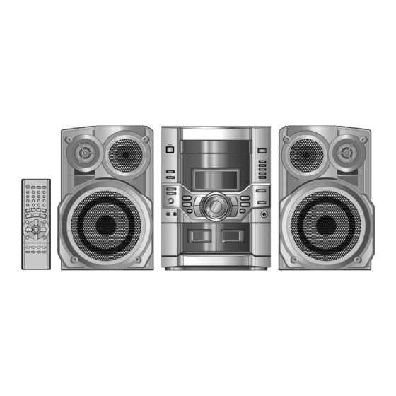
Page 9: Accessories
SA-VK61DGS 9 Accessories Remote control AC power supply cord FM indoor antenna AM indoor antenna Video cable... -
Page 10: Operation Procedures
SA-VK61DGS 10 Operation Procedures... - Page 11 SA-VK61DGS...
-
Page 12: Disc Information
SA-VK61DGS 11 Disc information... - Page 13 SA-VK61DGS...
-
Page 14: About Highmat
SA-VK61DGS 12 About HighMAT 12.1. What is HighMAT? This word combines the abbreviations of Matsushita Electric Industrial Co. Ltd. and High Performance Media Access Technology, and is a trademark of Microsoft Corporation. The products with the HighMAT logo shown below are made according to the HighMAT standard. -
Page 15: Outline Of The Highmat Standard
SA-VK61DGS · You can also play digital content on the disc, which was created in accordance with the HighMAT format with a conventional CD-ROM player. 12.4. Outline of the HighMAT standard 1. Recording medium · CD-R/CD-RW · Supports ISO 9660 Level Expanded Joliet ·... - Page 16 SA-VK61DGS · WMA, MP3 (MPEG-1 Audio Layer 3) 64 kbps - 160.999 kbps, 44.1 KHz, stereo, fixed bit rate/ variable bit rate. · WMA, V2 and above, excluding Lossless/Voice/Pro · JPEG: Max 6M pixel, Maximum file size: 3 MB 4. Limitations regarding the number of files on the media, etc. ·...
-
Page 17: Procedure For Repairing The Set
SA-VK61DGS 13 Procedure for repairing the set... -
Page 18: Distinguish The Trouble Cause
SA-VK61DGS 13.1. Distinguish the trouble cause How to distinguish the trouble 2. Diagnose if Optical Pickup Unit is faulty (refer to diagnosis of Optical Pickup Unit). 1. View mechanical part if visual damage occurred. 3. If mechanism and OPU are OK, it is P.C.B. Confirm the movement of mechanical parts assembly (tray ass’y, loading mechanism ass’y, etc.). - Page 19 SA-VK61DGS Cause 3 Possible fault 3. DVD Module (1) Circuit IC2501 (Tracking - pin 11 & 12) IC2501 (Focus - pin 13 & 14) IC2501 (spindle motor - pin 17, 18) IC2501 ( Traverse motor - pin 15, 16) FG unit (pin 1, 2 at FP5102) IC3001, Video Problem (pin 158 (Y/PY/G), pin 160 (CB/PB/B), pin 161 (CR/PR/R), pin 163 (Y) and pin 164 (C))
-
Page 20: Diagnosis Of Optical Pick-Up Unit
SA-VK61DGS 13.2. Diagnosis of Optical Pick-up Unit How to distinguish Laser destruction/damage Confirmation 1 Remove cover of mechanism block so that you will see the lens of optical pickup. Confirm emission of laser at the moment when power switch is turned on. If there is no laser emission, laser diode is faulty. - Page 21 SA-VK61DGS While pressing & hold “STOP” button on main unit, press “Display” button on the remote controller. Unit display laser current on FL. From the reading of display, you can judge if laser diode is damaged or not. Reading on the right side should be less than 70. If reading is more than 70, laser is damaged. How to confirm if Optical Pickup is OK Confirmation 1 1.
-
Page 22: Optical Pickup Self-Diagnosis And Replacement Procedure
SA-VK61DGS 14 Optical Pickup Self-Diagnosis and Replacement Procedure 14.1. Self-diagnosis This unit is equipped with the optical pickup self-diagnosis function and the tilt adjustment check function. Follow the procedure described below during repair in order to perform self-diagnosis and tilt adjustment effectively. Especially when “NO DISC” is displayed, be sure to apply the self-diagnosis function before replacing with an optical pickup. -
Page 23: Cautions To Be Taken During Replacement Of Optical
SA-VK61DGS 14.2. Cautions to Be Taken During Replacement of Optical Pickup and Spindle Motor Before replacing the optical pickup and spindle motor, check a total usage time respectively. Follow the checking method described below. Item Status and Key Function Display Checking DVD, CD laser usage time With the unit stopped and no disc inserted, T1_xxxx_yyyy... -
Page 24: Self-Diagnosis Function
SA-VK61DGS 15 Self-Diagnosis Function This unit is equipped with the self-diagnosis function, which displays an error when it occurs, for use during servicing. 15.1. Automatic Displayed Error Codes 15.1.1. Automatic Display Function For a power unit error, the code is automatically displayed. F61: Automatically displayed on the LCD of the player. -
Page 25: Dvd/Cd Self-Diagnosis Error Code Description
SA-VK61DGS 15.4. DVD/CD Self-Diagnosis Error Code Description Error Code State, Conditon Cause, Troubleshooting The disc tray cannot be opened: it closes spontaneously. Disc tray open/close detection switch (S1001) failure. (Check and replace) The disc tray cannot be closed: it opens spontaneously. Error Code Meaning Details... - Page 26 SA-VK61DGS Item Operational Details Display TO Exit Mode Condition and Key Function Jitter display While the player is Jitter display _yyy Press the STOP or stopped and no disc is Measures displays jitter. OPEN button. inserted, press Measurement repeated every : Jitter display mode hold down the second.
- Page 27 SA-VK61DGS Item Operational Details Display TO Exit Mode Condition and Key Function Measurement of CD While the player is Measurement of CD laser current _032 _032 Automatically exits laser current electricity stopped and no disc is electricity the mode after five inserted, press Measures CD laser current electricity...
-
Page 28: Tray Lock Function
SA-VK61DGS Item Operational Details Display TO Exit Mode Condition and Key Function Reset spindle While the usage time 2 Usage time 2 reset T2_00000 Automatically exits time is displayed, press and Spindle motor usage time the mode after five hold down the seconds. -
Page 29: Cautions To Be Taken During Servicing
SA-VK61DGS 16 Cautions To Be Taken During Servicing 16.1. Recovery after the dvd player is repaired · When Flash ROM or module(2) P.C.B. is replaced, carry out the recovery processing to optimize the drive. Playback the recovery disc to process the recovery automatically. ·... -
Page 30: Total Usage Time Display
SA-VK61DGS 2. The version of player is automatically checked and prompts if necessary. 3. Select version upgrade process using the cursor keys on the remote controller unit. (Select YES or NO) 4. a. If YES is selected, the process starts. b. -
Page 31: Disassembly And Assembly Of Main Component
SA-VK61DGS 17 Disassembly and Assembly of Main Component 17.1. Disassembly flow chart The following chart is the procedure for disassembling the casing and inside parts for internal inspection when carrying out the servicing. To assemble the unit, reverse the steps shown in the chart as below. -
Page 32: Disassembly Of Top Cabinet
SA-VK61DGS 17.2. Disassembly of Top Cabinet Step 1 Remove 3 screws each side and 5 screws at rear panel. Step 2 Lift up both sides of cabinet ass’y, push the cabinet ass’y toward the rear and remove the top cabinet. 17.3. - Page 33 SA-VK61DGS Step 1 Insert the gear tool into the hole on the underside of changer chasis and then rotate in the direction of arrow. The disc tray will be open. Step 4 Release the 2 claws, and then remove the Top Ornament Unit.
-
Page 34: Disassembly For Dvd Changer Unit
SA-VK61DGS 17.5. Disassembly for DVD changer unit · Follow the (Step 1) - (Step 2) of Item 17.2. 17.5.1. Disassembly of the DVD Module · Follow the Disassembly for the Top Ornament Unit of Item (1) P.C.B. 17.4. · Follow the (Step 1) - (Step 2) of Item 17.2. Step 1 Detach FFC Boards (FP5201, FP3202, FP3203 &... -
Page 35: Disassembly Of Main P.c.b., Power P.c.b., Transformer
SA-VK61DGS Step 2 Remove 2 screws at bottom chassis. Step 4 Remove the 8 screws. Step 3 Release the 2 claws, and then draw the front panel Step 5 Disconnect FFC board (CN601 & CN602). ass’y forward. Step 6 Draw the Panel P.C.B. forward to remove it. ·... -
Page 36: Terminal
SA-VK61DGS Step 1 Remove the 4 screws. Step 2 Disconnect connector CN950 & CN951. · Replacement of Power Amp IC Step 1 Remove the 2 screws fixed to the Power Amplifier IC. Step 2 Detach wire. NOTE: Insulate Power P.C.B. with insulation material to avoid short Step 2 Remove 2 screws fixed to the Power Amplifier IC and circuit. -
Page 37: Dvd Changer Unit Main Component Replacement
SA-VK61DGS Step 5 Fix back the bottom chasis with a screw as shown. 17.8. DVD Changer Unit Main Component Replacement Procedures 17.8.1. Replacement of the Traverse Deck · Follow the (Step 1) - (Step 2) of Item 17.2. · Follow the Disassembly for the Top Ornament Unit of Item 17.4. - Page 38 SA-VK61DGS Step 6 Remove the traverse deck ass’y from the timing lever. Caution: Step 11 Disengage the tabs from the traverse gear. When removing or inserting the traverse deck avoid touching the OPU lens and pressing onto the turntable. Step 12 Remove the traverse gear. Step 7 Remove 3 screws.
- Page 39 SA-VK61DGS · Note for installation of the DVD Module (1) P.C.B. Step 16 Remove the FFC board from the connector, and then remove the DVD Module (1) P.C.B. · Installation of the DVD Module (1) P.C.B. after replacement Step 1 Connect the FFC board. ·...
- Page 40 SA-VK61DGS 17.8.2. Replacement for the disc tray Step 1 Remove 4 screws. Step 2 Remove the upper plate. Step 3 Force the claw of timing lever. Step 3 Remove 3 screws. Step 4 Force the disc tray fully. Step 4 With lifting the claw in the direction of (1), draw the clamp SW P.C.B.
- Page 41 SA-VK61DGS Step 6 Insert the gear with hexagonal wrench into the hole. Step 7 Rotate the hexagonal wrench in the direction of arrow, and then open the disc tray fully. Step 1 Slide the drive rack fully in the direction of arrow. Step 2 Holding the drive rack not to move, install the disc tray.
- Page 42 SA-VK61DGS Step 4 Holding the disc tray manually, push the disc tray in the direction of the arrow. 17.8.3. Disassembly and reassembly for mechanism base drive unit Step 5 Release the 2 claws, and then remove the bottom SW · Follow the (Step 1) - (Step 9) of Item 17.8.2. P.C.B..
- Page 43 SA-VK61DGS Step 11 Lift up the left end of spindle base unit in the direction of arrow (1), and then remove the unit in the direction of arrow (2). Step 9 Pressing the claw (B) in the direction of arrow (1), force the connection lever in the direction of arrow (2).
- Page 44 SA-VK61DGS Step 3 Rotate the disc lever in the direction of arrow (1), draw the disc lever. Step 13 Remove the traverse relay gear, traverse cam gear and drive gear. [Dissassembly/reassembly for the spindle base unit] Step 1 Draw the 5 disc spacers. NOTE: Take care not to lose the disc lever spring.
- Page 45 SA-VK61DGS NOTE: Hold the loading stopper ass’y manually bacause it is flipped by spring. Step 8 Release the 2 claws, and then remove the relay gear A. Step 9 Release the 2 claws, and then remove the spindle shaft. Step 10 Remove the lower spindle spring with tweezers. Step 6 Remove the cushion spring.
- Page 46 SA-VK61DGS spread the hold bars of loading stopper and remove the UP/DOWN base. [Installation for loading stopper ass’y] Step 1 Align the claw of loading stoppers ass’y with the slot of spindle base. (Caution should be exercised when alignment of claw due to the size of claws.) Step 2 Lower the loading stopper ass’y, and then align the lower spindle with the trapezoid tooth of relay gear A.
- Page 47 SA-VK61DGS Step 1 Install the traverse cam gear. Step 2 Rotate the traverse cam gear to the direction of arrow. Step 4 Install the slide plate 2 to the mechanism base, and Step 3 Install the drive gear and traverse relay gear. then match to the connection lever.
- Page 48 SA-VK61DGS Step 7 Move the slide plate 1 to forward fully. Step 8 Install the rear lock. (The claw should be latched.) Step 9 Install the bottom SW P.C.B.. (The claw should be latched.) Step 10 Install the tray lock. (The claw should be latched.) Step 11 Remove the tray lock spring from hook,and then latch to the tray lock.
- Page 49 SA-VK61DGS Step 4 Unsolder the plunger terminals (2 points). Step 14 Install the tray base, traverse ass’y, mechanism cover Step 5 Unsolder the motor terminals (2 points). and upper plate. [Operation check after servicing] Check the proper operation of following items with gear and hexagonal screwdriver.
-
Page 50: Disassembly Of Deck Mechanism Unit
SA-VK61DGS 17.9. Disassembly of Deck Mechanism Unit · Follow the (Step 1) - (Step 2) of Item 17.2. · Follow the Disassembly for the Top Ornament Unit of Item 17.4. · Follow the Disassembly for the DVD changer unit of Item 17.5. - Page 51 SA-VK61DGS Step 14 Remove 2 screws. 17.9.1. Replacement for the CD motor ass’y, capstan belt A, capstan belt B and winding belt Step 1 Release the 2 claws, and then remove the head connector. Step 2 Remove 6 screws. Step 3 Remove the sub chassis. Step 5 Remove the flywheel R.
- Page 52 SA-VK61DGS Step 7 Put the capstan belt A temporarily as shown below. Step 2 Put the winding belt on the pulley temporarily. Step 3 Install the flywheel F. Step 4 Put the winding belt on the flywheel F. Step 5 Install the winding lever and spring while pressing the winding arm in the direction of arrow.
-
Page 53: Replacement For The Cassette Lid Ass 馳
SA-VK61DGS 17.10. Replacement for the cassette lid ass’y · Follow the (Step 1) - (Step 2) of Item 17.2. Step 1 Force the lever upward, open the cassette lid ass’y. (For DECK1 and DECK2) Step 10 Remove 3 screws. Step 2 Lift up the cassette lid ass’y in the direction of arrow. Step 11 Put the capstan belt B as shown below. -
Page 54: Counter-Measure For Tape Trouble
SA-VK61DGS 17.11. Counter-measure for tape trouble · Follow the (Step 1) - (Step 2) of Item 17.2. Step 1 If a cassette tape cannot be removed from the deck since the tape is caught by the capstan or pinch roller during playback or recording, rotate the flywheel F in the direction of the arrow to remove the tape. -
Page 55: Measurements And Adjustments
SA-VK61DGS 18 Measurements and Adjustments 18.1. Cassette Deck Section 18.1.2. Tape Speed Adjustment (Deck 1/2) · Measurement Condition 1. Set the tape edit button to “NORMAL” position. − − − − Reverse-mode selector switch: 2. Insert the test tape (QZZCWAT) to DECK 2 and playback −... -
Page 56: Tuner Section
SA-VK61DGS 18.1.4. Bias Frequency Adjustment (Deck 1/2) 1. Set the unit to “AUX” position. 2. Insert the Normal blank tape (QZZCRA) into DECK 2 and set the unit to “REC” mode (l use “REC/STOP” key). 3. Adjust L1002 so that the output frequency is within the standard value. -
Page 57: Alignment Points
SA-VK61DGS 18.3. Alignment Points 18.3.1. Cassette Deck Section 18.3.2. Adjustment Point... -
Page 58: Block Diagram
SA-VK61DGS 19 Block Diagram IC3051 C3ABPJ000017 64M SDRAM 2,4,5,7,8,10, 16,28, 21,24~27, 11,13,31,33,34, 59,71 60~66 36,37,39,40,42, 45,47,48,50,51, 53,54,56,74,76, 77,79,80,82,83,85 IC6251 C0CBCBE00003 REGULATOR TO MAIN BLOCK IC6261 IC6262 C0JBAA000001 C0JBAA000001 INVERTER INVERTER 2,3,5,6,8~10,12, 13,184,185,187,188, 210,212,214, 190~193,196,197, 216,217,219, 199~201,203~205,247, 207,208, 220,227~229, 249,251~253,255,256 243,246 231,235 AV DECODER MN2DS0002AP1... - Page 59 SA-VK61DGS 1~8, 18~25 32,34, 36,39 IC6301 29,31, DQ12 33,35, RFKFMV71W160 38,40, 16M FLASH 42,44 IC6201 C0EBE0000070 XRESET RESET IC TO FG UNIT FP2501 QR2045 SWITCH 19~22,27,28, 31,32,34~37, 94~97, 40,41,44,45 100~103 86~89 AV DECODER MN2DS0002AP1 IC3001...
- Page 60 SA-VK61DGS OPTICAL PICKUP DVDM LDOUT M2501 M2502 IC2501 C0GBG0000033 MOTOR DRIVE Q5115 Q5111 SUPPLY SUPPLY SWITCH SWITCH Q5225 Q5221 SWITCH SWITCH Q5211 SWITCH FILTER 121 120 AV DECODER MN2DS0002AP1 IC3001...
- Page 61 SA-VK61DGS TO MAIN BLOCK INVERTER SWITCH JK301 S-VIDEO C OUT Y OUT1 MUTING SWITCH Y OUT2 IC50 C9ZB00000377 CR OUT VIDEO BUFFER 7(8) CB OUT JK302 PY OUT1 PY OUT2 IC4201 MUTING C0FBBK000035 MIX OUT2 VIDEO ZFLAGA SWITCH 2CH D/A CONVERTER MIX OUT1 X6501...
- Page 62 SA-VK61DGS AM ANT FM ANT Z120 CF201 CF202 Q101 (RF AMP) Q1 Z101 FM IF AMP MIXER COIL COIL BUFFER (FM) DECODER RM AMP PHASE PILOT BUFFER CANCEL LEVEL S-CURVE STEREO SWITCH AM/FM BUFFER COMP TUNING DRIVE PILOT IC101 X102 LA1833NMNTLM FM/ AM IF AMP Z102...
- Page 63 SA-VK61DGS IC1001 AN7348S-E1 P.B. EQ/REC AMP/ ALC/TPS AMP 24(23) (DECK 1) Q1014(Q1015) P.B. HEAD 1(2) 20(5) BUFFER 22(3) 21(4) 17(8) (DECK 2) R/P HEAD 18(7) NOR/CrO & HI/LO LOGIC Q1012 Q1020 LOGIC L/H (Q1013) (Q1021) MUTING MUTING SWITCH RIPPLE LOGIC REJECTION REC/PB Q609...
- Page 64 SA-VK61DGS 27(4) DATA 29(2) IC301 C0JZAS000004 ANALOG SWITCH 19(12) VR602 Q606,Q607 Q900 LIMITER JK600 MIC1 24(7) IC702 C1BB00000801 22(9) KARAOKE IC 28(3) 25(6) 75(74) JK304 21(10) LINE JK900 MIC2 Q300 64(63), 7(1) 5(3) 65(62) MUTING CONTROL Q301 IC302 KIA4558FEL MUTING DUAL OP-AMP SWITCH 7(1)
- Page 65 SA-VK61DGS CLOCK DVD_PCNT DATA LIN(R) 15(13) LIN(R) IC307 C1BB00000782 IC703 6 CHANNEL C1BB00000574 VOLUME I/O EXPANDER IC308 BPL(R) 17(16) BYPASSL(R) C0AABB000117 OP-AMP Q312 Q317 31(32) 2(6) 1(7) MUTING MUTING LOUT(R) HP_MUTE CONTROL SWITCH WIDE PORT3 COUT DSP_PCNT LATCH Q308 MUTING CONTROL Q522 Q314...
- Page 66 SA-VK61DGS C0DBCFG00004 1.5V C0DBAMH00009 PCONT REGULATOR POWER SWITCH SUPPLY IC FILTER PCONT SWITCH C0DBAMH00009 POWER FILTER SUPPLY IC C0CBADG00005 CURRENT LIMITER REGUALTOR C0DBZHE00017 SWITCH POWER C0CBADG00005 SUPPLY IC REGULATOR Q801 SWITCH C0GAM0000005 MOTOR DRIVE D806 OUT1 OUT2 POWER SUPPLY CONTROL C0CBADG00005 REGULATOR Q101...
- Page 67 SA-VK61DGS 3(6) L OUT(R) JK953 FR_L(R) 21(20) L IN(R) D987(D984) Q546~ Q549,Q550 Q548 DCDET SWITCH, DISP HMUT SWITCH POWER SUPPLY IC500 RSN312H24-P Q545 POWER HIC SWITCH -VCC HI Q541,Q542 +VCC HI Q543, REGULATOR Q544 AC IN D501 REGULATOR -VCC LOW -Di SENS D500 +VCC LOW...
-
Page 68: Schematic Diagram
SA-VK61DGS 20 Schematic Diagram (All schematic diagrams may be modified at any time with the repair. development of the new technology) · Cover the parts boxes made of plastics with aluminium foil. Note: · Put a conductive mat on the work table. S501 : Voltage Selector Switch ·... -
Page 69: A) Dvd Module (1) Circuit
SA-VK61DGS 20.1. (A) DVD Module (1) Circuit SCHEMATIC DIAGRAM-1 : CD-DA SIGNAL LINE DVD MODULE (1) CIRCUIT : +B SIGNAL LINE IC2501 C0GBG0000033 MOTOR DRIVE BIAS1 LDCNT MUTE3 VIN1 R2502 VIN2 TRIN OPIN+ BIAS2 OPIN- LDIN R2503 OPOUT VIN3 GND(Pre) PREVCC C2508 C2506... - Page 70 SA-VK61DGS SCHEMATIC DIAGRAM-2 : CD-DA SIGNAL LINE DVD MODULE (1) CIRCUIT : +B SIGNAL LINE R2501 C2510 TP5101 TP5102 TP5103 DGND DGND R5107 C2513 C2503 R2507 TP5104 MUTE4 16V22 TP5113 D+5V D+5V R5108 C2505 C2509 C2502 CP5102 TRAYIN(D+5V) 16V10P 16V100 TP5105 M+9V M+9V...
-
Page 71: B) Dvd Module (2) Circuit
SA-VK61DGS 20.2. (B) DVD Module (2) Circuit SCHEMATIC DIAGRAM - 3 : CD-DA SIGNAL LINE DVD MODULE 2 (FORE) CIRCUIT : +B SIGNAL LINE QR2045 UNR511M00L SWITCH QR2045 R2046 CP2041 TC5240 LB5235 J0JBC0000015 TC5239 DGND R2045 DGND MUTE4(DGND) TC5238 MUTE4 HIND TC5237 D+5V... - Page 72 SA-VK61DGS SCHEMATIC DIAGRAM - 4 DVD MODULE 2 (FORE) CIRCUIT : +B SIGNAL LINE KMODE RA6201 (4.7K x 2) CP2019 C2021 4700P R2016 CP2016 8.2K DAC0 C2015 1000P R2018 CP2018 8.2K DAC1 C2016 820P R2012 CP2011 CP2012 7.5K SPDRV C2011 R2014 CP2013 CP2014...
- Page 73 SA-VK61DGS SCHEMATIC DIAGRAM - 5 DVD MODULE 2 (DV1) CIRCUIT : +B SIGNAL LINE HIND EXADR (20) HIND EXADR (19) HIND EXADR (18) HIND EXADR (17) HIND EXADR (16) C3003 HIND EXADT (15) HIND EXADT (14) HIND EXADT (13) MDQ(3) HIND EXADT (12) MDQ(12)
- Page 74 SA-VK61DGS SCHEMATIC DIAGRAM - 6 : CD-DA SIGNAL LINE DVD MODULE 2 (DV1) CIRCUIT : +B SIGNAL LINE RA3010 RA3003 RA3004 RA3005 (82 x 4) (82 x 4) (22 x 2) (82 x 4) VDD33 MDQ27 MDQ11 MDQ21 MDQ3 MDQ26 VDD33 MDQ12 MDQ25...
- Page 75 SA-VK61DGS SCHEMATIC DIAGRAM - 7 : CD-DA SIGNAL LINE : DVD (AUDIO) SIGNAL LINE DVD MODULE 2 (DV1) CIRCUIT : +B SIGNAL LINE : DVD (VIDEO) SIGNAL LINE L3101 LB3001 G1C100K00020 J0JHC00000045 D+3.3V FORE/HIND D+1.5V HIND C3001 C3002 LB3002 6.3V330 6.3V330 J0JHC00000045 RA3011...
- Page 76 SA-VK61DGS SCHEMATIC DIAGRAM - 8 DVD MODULE 2 (DV1) CIRCUIT : +B SIGNAL LINE C3051 MDQ(0) MDQ(15) DQ15 C3052 VCCQ VSSQ MDQ(14) MDQ(1) DQ14 MDQ(2) MDQ(13) DQ13 C3062 VSSQ VCCQ MDQ(3) MDQ(12) DQ12 MDQ(4) MDQ(11) DQ11 C3053 VCCQ VSSQ MDQ(10) MDQ(5) DQ10 MDQ(9)
- Page 77 SA-VK61DGS SCHEMATIC DIAGRAM - 9 DVD MODULE 2 (HIND) CIRCUIT : +B SIGNAL LINE LB6301 J0JHC0000045 IC6301 RFKFMV71W160 16M FLASH CP6317 CP6318 EXDAT (15) EXADR (16) CP6316 EXDAT (14) XBYTE CP6315 EXDAT (13) CP6335 CP6314 EXDAT (12) DQ15/A-1 EXTRG0 CP3005 CP6313 EXDAT (11) MONI (7)
- Page 78 SA-VK61DGS SCHEMATIC DIAGRAM - 10 DVD MODULE 2 (HIND) CIRCUIT : +B SIGNAL LINE IC6251 C0CBCBE00003 REGULATOR DV1/FORE D+3.3V C6252 C6253 C6251 0.01 IC6261 C0JBAA000001 INVERTER LB6261 J0JBC0000015 RA6261 R6261 (10K x 2) CP6262 C6261 DSPLCLK_DV1 IC6261 LB3201 D0GB101JA002 DSPCLK-MINI IC6262 C0JBAA000001 INVERTER...
- Page 79 SA-VK61DGS SCHEMATIC DIAGRAM - 11 DVD MODULE 2 (HIND) CIRCUIT : +B SIGNAL LINE : DVD (VIDEO) SIGNAL LINE DGND FL6251 F1J1E1040022 TP6272 M+9V FORE M+9V TP6273 M+9V FORE MGND MGND FL6252 MGND F1H0J1050018 TP6274 D+5V FORE D+5V C6255 D+5V 6.3V100 TP6275 DGND...
- Page 80 SA-VK61DGS SCHEMATIC DIAGRAM - 12 DVD MODULE (2) (AUDIO DAC) CIRCUIT : MAIN SIGNAL LINE : +B SIGNAL LINE DMIXOUT SBO1 SBT1 STBDAC SRCK LRCK IC4201 R4201 C0FBBK000035 2CH D/A CONVERTER DATA LRCK C4209 DGND L4211 LB4200 C4202 IC4201 J0JBC0000015 G1C220KA0038 10V10 ZEROL...
- Page 81 SA-VK61DGS SCHEMATIC DIAGRAM - 13 : +B SIGNAL LINE DVD MODULE (2) (AUDIO DAC) CIRCUIT : MAIN SIGNAL LINE FP4202 AGND FL4201 F1H0J1050018 AGND TC4218 TC4215 AGND AGND AGND TC4220 LB4215 AGND J0JCC0000119 MAIN CIRCUIT TC4278 MIXR TC4217 (CN303) ON AGND LB4214 SCHEMATIC...
-
Page 82: C) Main Circuit & (D) Tuner Extent Circuit
SA-VK61DGS 20.3. (C) Main Circuit & (D) Tuner Extent Circuit SCHEMATIC DIAGRAM - 14 : MIC SIGNAL LINE : AM/FM SIGNAL LINE : AUX SIGNAL LINE : MAIN SIGNAL LINE : PLAYBACK SIGNAL LINE MAIN CIRCUIT : +B SIGNAL LINE : RECORD SIGNAL LINE TUNER_GND +15V... - Page 83 SA-VK61DGS SCHEMATIC DIAGRAM - 15 : AUX SIGNAL LINE : -B SIGNAL LINE : PLAYBACK SIGNAL LINE : MAIN SIGNAL LINE MAIN CIRCUIT : +B SIGNAL LINE : RECORD SIGNAL LINE : AM/FM SIGNAL LINE Q300 B1GFGCAA0001 MUTING CONTROL C205 R211 50V3.3 C203...
- Page 84 SA-VK61DGS SCHEMATIC DIAGRAM - 16 MAIN CIRCUIT : +B SIGNAL LINE : MAIN SIGNAL LINE R273 100K B0ACCK000005 B0ACCK000005 R317 5.6K Q15, Q16 B1GBCFJN0021 MUTING SWITCH 1 2 3 4 16 17 18 19 20 21 1 2 3 4 16 17 18 19 20 21 CN602 CN303...
- Page 85 SA-VK61DGS SCHEMATIC DIAGRAM - 17 : -B SIGNAL LINE MAIN CIRCUIT : +B SIGNAL LINE : MAIN SIGNAL LINE C724 C725 R725 16V100 C415 R463 4.7K 50V1 LIN4 ELRI/O SYNC R468 C464 LIN3 3.3K 1000P LIN2 GNDR C215 R263 LIN1 VDDR 4.7K 50V1...
- Page 86 SA-VK61DGS SCHEMATIC DIAGRAM - 18 : -B SIGNAL LINE : DVD (VIDEO) SIGNAL LINE MAIN CIRCUIT : +B SIGNAL LINE : MAIN SIGNAL LINE D312, 313, 315 D303 B0ACCK000005 B0BC5R000009 R343 R344 R345 C353 R346 C764 D312 D303 PORT1 DVDD Q700 D313 R347...
- Page 87 SA-VK61DGS SCHEMATIC DIAGRAM - 19 MAIN CIRCUIT : +B SIGNAL LINE : DVD (VIDEO) SIGNAL LINE ELJFCR39KF IC50 ELESN220JA C9ZB00000377 VIDEO BUFFER 0.01 2.2K B1GBCFJN0021 INVERTER SWITCH 100K 100K 100K 0.01 100K 100K 100K 470P 0.01 1000P 1000P C302 16V10 1000P 470P JK305...
- Page 88 SA-VK61DGS SCHEMATIC DIAGRAM - 20 : -B SIGNAL LINE MAIN CIRCUIT : +B SIGNAL LINE Q801 B1GBCFJA0015 SWITCH Q801 R900 R901 R902 C823 4.7K B1GDCFJJ0023 SWITCH G0A100G00005 6.3V220 16V10 6.3V220 C0CBADG00005 C0CBADG00005 5V REGULATOR 5V REGULATOR 25V220 16V10 G0A101G00022 6.3V100 C0DBAMH00009 C0DBZHE00017 C0DBCFG00004...
- Page 89 SA-VK61DGS SCHEMATIC DIAGRAM - 21 : -B SIGNAL LINE MAIN CIRCUIT : +B SIGNAL LINE : MAIN SIGNAL LINE C463 R459 16V10 D700,701 B0AACK000005 R462 2.7K C456 50V4.7 R262 2.7K C256 50V4.7 Q321 R727 C263 R259 B1ABCF000131 16V10 R724 C733 R729 C732 16V10...
- Page 90 SA-VK61DGS SCHEMATIC DIAGRAM - 22 : -B SIGNAL LINE MAIN CIRCUIT : +B SIGNAL LINE : MAIN SIGNAL LINE R265 3.3K Q314 R361 R338 MUTE_A Q308 Q308 B1GFGCAA0001 MUTING CONTROL R360 R243 R443 C362 50V22 C242 R245 R248 R465 50V4.7 2.7K 3.3K Q314, 317...
- Page 91 SA-VK61DGS SCHEMATIC DIAGRAM - 23 : -B SIGNAL LINE MAIN CIRCUIT : +B SIGNAL LINE : MAIN SIGNAL LINE R100 R101 R103 CN309 VREF+ CHG_CW CHG_CW CHG_HALF CHG_HALF CHG_CCW CHG_CCW R108 CLAMP CHG_AD1 R109 OPEN CHG_AD2 CD LOADING R104 CHG_SW C100 CIRCUIT 0.47...
- Page 92 SA-VK61DGS SCHEMATIC DIAGRAM - 24 : MIC SIGNAL LINE MAIN CIRCUIT : +B SIGNAL LINE : MAIN SIGNAL LINE R633 R632 C623 4.7K 1000P C622 IC703 IC703 C1BB00000574 I/O EXPANDER C621 C620 R626 R625 SERD SERA DVD_PCNT KA_ROUT KA_LOUT KA_RIN C270 16V10 KA_LIN...
- Page 93 SA-VK61DGS SCHEMATIC DIAGRAM - 25 : -B SIGNAL LINE MAIN CIRCUIT : +B SIGNAL LINE L370 G0C221KA0007 DCDET R399 Q375 B1ABCF000011 C375 DCDET SWITCH 6.3V330 CN305 D377 B0ACCK000005 R379 Q374 Q374 100K B1ADCF000001 FAN MOTOR DRIVE R378 D376 D375 C390 R377 220K D375, 376...
-
Page 94: E) Panel Circuit, (F) Led Circuit & (G) Tact Switch Circuit
SA-VK61DGS 20.4. (E) Panel Circuit, (F) LED Circuit & (G) Tact Switch Circuit SCHEMATIC DIAGRAM - 26 : MIC SIGNAL LINE : PLAYBACK SIGNAL LINE PANEL CIRCUIT : +B SIGNAL LINE : RECORD SIGNAL LINE R681 SW5V S601 R617 POWER R612 AGND AGND... - Page 95 SA-VK61DGS SCHEMATIC DIAGRAM - 27 : -B SIGNAL LINE PANEL CIRCUIT : +B SIGNAL LINE FL600 A2BD00000071 FL DISPLAY C641 2 3 4 5 6 7 8 9 10 11 12 13 14 15 16 17 18 19 20 21 22 23 24 25 26 27 28 29 30 31 32 33 34 35 36 37 38 39 40 41 42 43 44 45 46 47 48 49 50 51 52 53 54 50V22 C642 50V22...
- Page 96 SA-VK61DGS SCHEMATIC DIAGRAM - 28 : -B SIGNAL LINE PANEL CIRCUIT : +B SIGNAL LINE : MAIN SIGNAL LINE R712 100K R713 100K R714 100K R715 100K R716 100K R717 100K R718 100K R719 100K R720 100K R721 100K R722 100K R723 100K...
- Page 97 SA-VK61DGS SCHEMATIC DIAGRAM - 29 POWER CIRCUIT : MAIN SIGNAL LINE : PLAYBACK SIGNAL LINE (CN954) ON : -B SIGNAL LINE : RECORD SIGNAL LINE SCHEMATIC DIAGRAM - 37 PANEL CIRCUIT : +B SIGNAL LINE : MIC SIGNAL LINE H600/W600 1 2 3 4 5 6 7 R676 SYNC...
-
Page 98: H) Tuner Circuit
SA-VK61DGS 20.5. (H) Tuner Circuit SCHEMATIC DIAGRAM - 30 : +B SIGNAL LINE : AM SIGNAL LINE TUNER CIRCUIT : FM OSC SIGNAL LINE : AM OSC SIGNAL LINE : FM SIGNAL LINE TUNER PACK CIRCUIT 2SK544 2SC2786M C103 R107 5.6P RF AMP FM MIXER... - Page 99 SA-VK61DGS SCHEMATIC DIAGRAM - 31 : AM SIGNAL LINE : AM OSC SIGNAL LINE TUNER CIRCUIT : +B SIGNAL LINE : FM SIGNAL LINE : FM/AM SIGNAL LINE R104 CF202 R101 RLFFETWND01M R121 Q106 B1GCCFJJ0015 TUNER SUPPLY C120 SWITCH 16V10 R143 C138 0.01...
-
Page 100: J) Deck Circuit & (K) Deck Mechanism Circuit
SA-VK61DGS 20.6. (J) Deck Circuit & (K) Deck Mechanism Circuit SCHEMATIC DIAGRAM - 32 : +B SIGNAL LINE : RECORD SIGNAL LINE DECK CIRCUIT : PLAYBACK SIGNAL LINE R1038 R1039 R1055 4.7K 2.2K C1038 220P R1098 C1044 R1015 C1034 10V33 50V3.3 C1032 IC1001... - Page 101 SA-VK61DGS SCHEMATIC DIAGRAM - 33 PANEL CIRCUIT : +B SIGNAL LINE (CP603) ON SCHEMATIC : RECORD SIGNAL LINE DIAGRAM - 26 DECK CIRCUIT : PLAYBACK SIGNAL LINE CN1001 C1054 50V3.3 R1060 C1064 50V3.3 R1095 R1091 Q1017 100K 2.2K R1057 W1002 R1094 R1049 C1051...
-
Page 102: L) Power Supply Circuit
SA-VK61DGS 20.7. (L) Power Supply Circuit SCHEMATIC DIAGRAM - 34 : +B SIGNAL LINE POWER SUPPLY CIRCUIT : -B SIGNAL LINE : MAIN SIGNAL LINE IC500 RSN312H24-P POWER HIC C503 820P R510 C506 C502 820P 0.01 C510 R512 R509 C509 R505 R506 R502... - Page 103 SA-VK61DGS SCHEMATIC DIAGRAM - 35 : +B SIGNAL LINE POWER SUPPLY CIRCUIT : -B SIGNAL LINE : MAIN SIGNAL LINE Q522 Q548 B1AAGC000007 KTC3199GRTA Q548 MUTING SWITCH SWITCH R563 R530 R564 Q522 100K D520 - 523 C543 B0BA01900005 50V2.2 D520 D522 D545 B0AACK000004...
-
Page 104: M) Power Circuit
SA-VK61DGS 20.8. (M) Power Circuit SCHEMATIC DIAGRAM - 36 : +B SIGNAL LINE POWER CIRCUIT : -B SIGNAL LINE : MAIN SIGNAL LINE POWER SUPPLY CIRCUIT POWER SUPPLY CIRCUIT (CP502) ON (H500/W500) ON SCHEMATIC DIAGRAM - 34 SCHEMATIC DIAGRAM - 35 CN956 CN958 1 2 3 4 5 6... - Page 105 SA-VK61DGS SCHEMATIC DIAGRAM - 37 : +B SIGNAL LINE POWER CIRCUIT : -B SIGNAL LINE D951 - 954 B0HARM000017 D958 D957 B0FBAM000009 B0FBAM000009 250V 6.3A TRANSFORMER C951 C952 CIRCUIT (CN950) ON 250V 6.3A SCHEMATIC DIAGRAM - 38 D969, 971 - 973 B0HARM000017 H950/ W950...
- Page 106 SA-VK61DGS 20.9. (N) Transformer Circuit, (O) AC Inlet Circuit, (P) Voltage Selector Circuit, (Q) CD Loading Circuit, (R) CD Detect Circuit & (S) Spindle Position Circuit SCHEMATIC DIAGRAM - 38 : +B SIGNAL LINE TRANSFORMER CIRCUIT VOLTAGE SELECTOR CIRCUIT 240V 220-230V 127V 110V...
-
Page 107: Printed Circuit Board
SA-VK61DGS 21 Printed Circuit Board 21.1. (A) DVD Module (1) P.C.B. (Component & Foil Side) DVD MODULE (1) C5151 FP5101 P.C.B (REP3406B-N) D5151 TC5121 TC5101 TC5115 TC5120 C5102 C5101 LB5101 TC5109 C5123 R5115 C5103 TC5127 TC5107 RA5103 R5114 TC5105 TC5116 TC5117 R5113 R5105... -
Page 108: B) Dvd Module (2) P.c.b. (Side A & B)
SA-VK61DGS 21.2. (B) DVD Module (2) P.C.B. (Side A & B) DVD MODULE(2) P.C.B (REP3587H) L2001 C2001 LB5201 LB5204 C2003 LB5205 CP3013 LB5207 LB5208 LB5211 LB5213 CP5231 R5233 R5234 CP5232 L2002 C2002 LB5220 R2013 R2011 R2015 LB5228 RA2025 TP6565 RA3042 LB5233 R2045 CP4202... - Page 109 SA-VK61DGS TL3012 C6262 LB6261 C6261 L2001 TL6205 C2001 CP2023 TL6207 IC6261 IC6262 TL6202 TL6208 RA6201 TL6206 TL6203 TL6204 CP6262 CP6263 C3013 C2003 C3014 CP3013 IC6351 R6261 CP4204 CP6201 CP4203 C6301 IC3001 IC6301 RA3012 RA3002 RA3001 R3001 RA3004 RA3003 RA3005 RA3009 RA3010 RA3011 C6561...
- Page 110 SA-VK61DGS DVD MODULE(2) P.C.B (REP3587H) TP6205 TP6207 RA6261 TP6208 TP6206 LB6301 CP6242 C2057 R6351 TC6201 C2058 IC6201 C3012 C2032 C2031 C3011 1 2 3 C3009 C2005 CP6334 C2036 C2006 CP6326 C2037 R2018 C3102 R2033 CP6333 CP6335 C3105 C3031 C3103 C3107 CP3005 R3104 CP3003...
- Page 111 SA-VK61DGS Q5211 CP5211 TC5201 C5201 TC5202 C5231 R5231 TC5242 TC5203 C5232 R5232 C2057 TC5243 TC5204 TC5206 LB5206 TC5205 TC5209 LB5210 TC5207 C2058 TC5244 TC5208 C2031 C2032 TC5211 LB5212 C2033 C2023 TC5213 LB5215 TC5216 C2021 LB5217 TC5220 TC5217 TC5219 TC5215 LB5219 TC5218 C2015 TC5221...
-
Page 112: C) Main P.c.b
SA-VK61DGS 21.3. (C) Main P.C.B. MAIN P.C.B J561 J559 J562 J207 Q371 (REPX0376K) J280 J261 Q370 J273 J266 J270 J545 J206 CN306 CN304 CN303 Q101 Q100 R101 R103 R107 J265 J217 J478 J479 J301 J428 J529 J528 J216 J360 CN309 J431 J482 J258... - Page 113 SA-VK61DGS J561 J562 Q375 Q371 J279 R399 D371 C375 C391 Q372 D377 Q374 D370 D376 Q370 R374 D375 J273 R373 J270 JK302 R376 Q373 J217 J428 CN305 J528 J216 J276 J404 J219 J362 L370 J361 J527 IC50 JK301 J278 J272 JK305 J277 J268...
-
Page 114: D) Tuner Extent P.c.b., (F) Led P.c.b. & (G) Tact P.c.b
SA-VK61DGS 21.4. (D) Tuner Extent P.C.B., (F) LED P.C.B. & (G) Tact P.C.B. TUNER EXTENT P.C.B LED P.C.B (REPX0376K) (REPX0378N) CP702 CP703 W601B R649 TACT P.C.B (REPX0378N) VOLUME S904 S901 S902 R901 R902 CD PLAY S905 S910 STOP DISPLAY VR600 S903 TUNER/BAND S906... -
Page 115: E) Panel P.c.b
SA-VK61DGS 21.5. (E) Panel P.C.B. PANEL P.C.B (REPX0378N) C634 C636 IC604 S606 R731 OPEN/CLOSE J642 J602 S607 DISC1 J603 D621 D622 S608 S609 DISC2 FL600 DISC3 C661 C641 D623 1 2 3 5 6 7 8 9 10 11 12 13 14 15 16 17 18 19 20 21 22 23 24 25 26 27 28 29 30 31 32 33 34 35 36 37 38 39 40 41 42 43 44 45 46 47 C659 W601A C640... - Page 116 SA-VK61DGS D600 S601 POWER H600 /W600 J692 J693 SENSOR R677 J648 C642 J605 R705 1 32 33 34 35 36 37 38 39 40 41 42 43 44 45 46 47 48 49 50 51 52 53 54 S602 R656 R707 Q603 D626...
-
Page 117: H) Tuner P.c.b. & (I) Tuner Pack P.c.b
SA-VK61DGS 21.6. (H) Tuner P.C.B. & (I) Tuner Pack P.C.B. TUNER P.C.B (REPX0373C) C130 R111 R113 R114 JK101 J107 X103 R137 R136 C110 R135 R134 J122 IC102 R151 R133 R129 R117 C124 R138 TO TUNER PACK P.C.B C150 R132 J105 C122 R105 R127... -
Page 118: J) Deck P.c.b. & (K) Deck Mechanism P.c.b
SA-VK61DGS 21.7. (J) Deck P.C.B. & (K) Deck Mechanism P.C.B. DECK P.C.B. DECK MECHANISM P.C.B. (REPX0331A) (REPX0321B) IC1004 Q1001 C1006 R1006 C1009 R1005 C1003 J1000 CS1002 TP10 J1002 L1002 TP11 Q1007 R1004 R1001 R1008 J1003 TP12 C1002 C1026 C1011 C1021 C1020 S951 C1016... -
Page 119: L) Power Supply P.c.b
SA-VK61DGS 21.8. (L) Power Supply P.C.B. POWER SUPPLY P.C.B (REPX0377F) Q540 9 10 11 12 13 14 15 16 17 18 19 20 21 22 J583 Q542 J542 IC500 R511 C503 H500 C511 C502 /W500 J537 J599 J516 J534 J552 D521 J622 J593... - Page 120 SA-VK61DGS J625 J602 Q540 IC501 9 10 11 12 J611 J583 Q542 J542 J541 J612 J556 J566 J626 R525 J579 J517 R524 J608 C525 Q544 J521 R550 J531 R543 J576 J512 Q541 R542 D542 R545 D541 D545 R517 J529 R546 R549 R548 Q547...
-
Page 121: M) Power P.c.b
SA-VK61DGS 21.9. (M) Power P.C.B. POWER P.C.B (REPX0377F) W952 J962 J987 T6.3AL Q951 J925 C958 C959 D962 R951 R950 Q950 C950 J914 R990 Q953 J903 C993 J913 D957 C990 D960 J912 H951/W951 D958 C952 J948 D959 C957 J993 J620 D966 J994 J934 J995... - Page 122 SA-VK61DGS J976 J915 J962 R960 J987 J618 Q951 C963 C960 J925 CN954 C958 W953 C959 D962 R994 R951 R950 D979 J914 J963 J944 D957 R531 C952 J932 J942 J964 J965 R992 J978 CN958 12 11 10 J993 J956 J994 J958 J995 J959 J916...
-
Page 123: N) Transformer P.c.b
SA-VK61DGS 21.10. (N) Transformer P.C.B. TRANSFORMER P.C.B (REPX0379C) RL502 D950 CN951 CN950 (YEL) (D.BLU) (BWN) (ORG) (BLK) (PUR) (L.BLU) T501(MAIN TRANSFORMER) SECONDARY PRIMARY CAUTION RISK OF ELECTRIC SHOCK AC VOLTAGE LINE. PLEASE DO NOT TOUCH THIS P.C.B... -
Page 124: O) Ac Inlet P.c.b. & (P) Voltage Selector P.c.b
SA-VK61DGS 21.11. (O) AC Inlet P.C.B. & (P) Voltage Selector P.C.B. VOLTAGE SELECTOR AC INLET P.C.B (REPX0379C) P.C.B (REPX0379C) D.BLU L.BLU J491 250V T3.15AL CN953 J492 J493 J494 S501 VOLTAGE J495 SELECTOR T502 SUB-TRANSFORMER JK500 L500 J584 AC IN J585 110V 127V 220V-230V... -
Page 125: Spindle Position P.c.b
SA-VK61DGS 21.12. (Q) CD Loading P.C.B., (R) CD Detect P.C.B. & (S) Spindle Position P.C.B. CD LOADING P.C.B (REP2578A-N) 2 3 4 5 6 7 8 9 10 OPEN PUSH PUSH SPINDLE POSITION P.C.B CD DETECT P.C.B (REP2578A-N) (REP2578A-N) LOAD... -
Page 126: Wiring Connection Diagram
SA-VK61DGS 22 Wiring Connection Diagram TACT SWITCH P.C.B. SOLDER SIDE VOLUME LED P.C.B. SOLDER SIDE VR600 W601B 1 ..8 CP900 H901 /W901 SENSOR H600/ W600 W601A 26 ... . . 1 15 . - Page 127 SA-VK61DGS VOLTAGE SELECTOR CD LOADING P.C.B. P.C.B. L.BLU CD DETECT P.C.B. D.BLU CN953 SOLDER SIDE S501 VOLTAGE SOLDER SIDE SELECTOR AC INLET P.C.B. SOLDER SIDE T502 SOLDER SIDE SUB-TRANSFORMER AC IN 110V L500 127V 220~230V 240V 7 ..1 50/60HZ CN951 RL502...
-
Page 128: Illustration Of Ics, Transistors And Diodes
SA-VK61DGS 23 Illustration of ICs, Transistors and Diodes AN7348S-E1 (24P) C1BB0000086(18P) RSN312H24-P C1DB00000980(16P) C0JZAS000004(30P) C0EBE0000070(100P) C0GBG0000033(28P) C9ZB00000377(32P) C1BB00000801(80P) KIA4558FEL(8P) C1BB00000574 (16P) C2HBZC000013(80P) C1BB00000782(42P) LA1833NMNTLM (24P) MN2DS0002AP1(208P) LC72131MDTRM (20P) M62456FPE1 (24P) C0FBBK000035 (16P) C0GAM0000005 CNB13030R2AU C0JBAA000001 C0AABB000117 C3EBGZ000001 (8P) C0DBCFG00004 C0CBCBE00003 C0DBAMH00009 C3FBMD000134 2SD1819A0L... -
Page 129: Terminal Function Of Ic
SA-VK61DGS 24 Terminal Function of IC 24.1. IC600 (C2BBHF000076 ) Pin No. Mark Function System Microprocessor MUTE_A Audio Mute Output Pin No. Mark Function PLLCE PLL CE EECS EEPROM Chip Select DSP_CS DSP CS SERA EXP_DECK_CK/EXP2 DSP_RST DSP IC Reset Output _CK/EE_CK SERE DSP/6CH... -
Page 130: Parts Location And Replacement Parts List
SA-VK61DGS 25 Parts Location and Replacement Parts List Notes: · Important safety notice: Components identified by mark have special characteristics important for safety. Furthermore, special parts which have purposes of fire-retardent (resistors), high-quality sound (capacitors), low noise (resistors), etc are used. When replacing any of these components, be sure to use only manufacturer’s specified parts shown in the parts list. -
Page 131: Deck Mechanism (Raa3412-S)
SA-VK61DGS 25.1. Deck Mechanism (RAA3412-S) 25.1.1. Deck Mechanism Parts Location... - Page 132 SA-VK61DGS...
- Page 133 SA-VK61DGS 25.1.2. Deck Mechanism Parts List Ref. No. Part No. Part Name & Description Remarks CASSETTE DECK RED0071 R/P HEAD BLOCK UNIT RED0072 P/B HEAD BLOCK UNIT RDG0300 REEL BASE GEAR RDG0301 WINDING RELAY GEAR RDK0026 MAIN GEAR RDR0029-3 RELAY PULLEY RDV0033-4 WINDING BELT RDV0034-1...
-
Page 134: Cd Loading Mechanism (Rd-Dac036-S)
SA-VK61DGS 25.2. CD Loading Mechanism (RD-DAC036-S) 25.2.1. CD Loading Mechanism Parts Location... - Page 135 SA-VK61DGS...
- Page 136 SA-VK61DGS...
- Page 137 SA-VK61DGS 25.2.2. CD Loading Mechanism Parts List Ref. No. Part No. Part Name & Description Remarks Ref. No. Part No. Part Name & Description Remarks TRAVERSE DECK RHD17044 DRIVE RACK SCREW RMC0415 ADJUST SPRING HOLDER RML0517 TIMING LEVER RME0319 TRV GEAR SPRING RML0516 PLUNGER LEVER RME0320...
-
Page 138: Cabinet
SA-VK61DGS 25.3. Cabinet 25.3.1. Cabinet Parts Location... - Page 139 SA-VK61DGS...
- Page 140 SA-VK61DGS...
-
Page 141: Electrical Parts List
SA-VK61DGS 25.3.2. Cabinet Parts List Ref. No. Part No. Part Name & Description Remarks Ref. No. Part No. Part Name & Description Remarks CABINET AND CHASSIS RHD30078 SCREW RJFX0003 PCB HOLDER REEX0202 10P FFC RKA0059-K LEG RUBBER REEX0273 30P FFC WIRE RKFX0093-K CASS. - Page 142 SA-VK61DGS Ref. No. Part No. Part Name & Description Remarks Ref. No. Part No. Part Name & Description Remarks B1GDCFJJ0023 TRANSISTOR Q1020 B1ABEB000001 TRANSISTOR B1GBCFJN0021 TRANSISTOR Q1021 B1ABEB000001 TRANSISTOR B1GDCFGA0014 TRANSISTOR Q5111 B1BDBF000004 TRANSISTOR B1GBCFJN0021 TRANSISTOR Q5115 B1BDBF000004 TRANSISTOR B1GBCFJN0021 TRANSISTOR Q5211 UNR212100L...
- Page 143 SA-VK61DGS Ref. No. Part No. Part Name & Description Remarks Ref. No. Part No. Part Name & Description Remarks D613 B0BA5R600016 DIODE LB5101 J0JHC0000045 CHIP INDUCTOR D614 B0ACCE000003 DIODE LB5105 J0JBC0000015 CHIP INDUCTOR D615 B0ACCE000003 DIODE LB5106 J0JBC0000015 CHIP INDUCTOR D616 MA2C700A0F DIODE...
- Page 144 SA-VK61DGS Ref. No. Part No. Part Name & Description Remarks Ref. No. Part No. Part Name & Description Remarks RSH1A91ZA-A SW CD J0JBC0000041 CHIP INDUCTOR K0L1BB000005 SW LOAD J0JBC0000041 CHIP INDUCTOR SW2501 RSH1A048-A SW LEAF J0JBC0000041 CHIP INDUCTOR J0JBC0000041 CHIP INDUCTOR CONNECTORS L370 G0C221KA0007...
- Page 145 SA-VK61DGS Ref. No. Part No. Part Name & Description Remarks Ref. No. Part No. Part Name & Description Remarks K5D632BK0007 6.3A FUSE ERJ3GEY0R00V 0 1/16W ERJ3GEY0R00V 0 1/16W FUSE HOLDERS ERJ3GEY0R00V 0 1/16W ERJ3GEY0R00V 0 1/16W EYF52BC FUSE HOLDER ERJ3GEY0R00V 0 1/16W EYF52BC FUSE HOLDER...
- Page 146 SA-VK61DGS Ref. No. Part No. Part Name & Description Remarks Ref. No. Part No. Part Name & Description Remarks ERJ3GEYJ104V 100K 1/16W R212 D0GB272JA002 2.7K 1/16W ERJ3GEYJ104V 100K 1/16W R213 ERJ3GEY0R00V 0 1/16W ERJ3GEYJ104V 100K 1/16W R214 ERJ3GEYJ103V 10K 1/16W ERJ3GEYJ104V 100K 1/16W R215...
- Page 147 SA-VK61DGS Ref. No. Part No. Part Name & Description Remarks Ref. No. Part No. Part Name & Description Remarks R399 ERJ3GEYJ103V 10K 1/16W R531 ERDS2TJ223T 22K 1/4W R401 ERJ3GEYJ473V 47K 1/16W R540 ERD2FCVJ4R7T 4.7 1/4W R402 D0GB100JA002 10 1/16W R541 ERDS2TJ272T 2.7K 1/4W R403...
- Page 148 SA-VK61DGS Ref. No. Part No. Part Name & Description Remarks Ref. No. Part No. Part Name & Description Remarks R652 ERDS2TJ101T 100 1/4W R714 ERDS2TJ104T 100K 1/4W R653 ERDS2TJ472T 4.7K 1/4W R714 ERJ3GEYJ103V 10K 1/16W R654 ERDS2TJ474T 470K 1/4W R715 ERDS2TJ104T 100K 1/4W R655...
- Page 149 SA-VK61DGS Ref. No. Part No. Part Name & Description Remarks Ref. No. Part No. Part Name & Description Remarks R923 ERDS2TJ223T 22K 1/4W R1057 ERJ3GEYJ222V 2.2K 1/16W R924 ERDS2TJ123T 12K 1/4W R1058 D0GB272JA002 2.7K 1/16W R925 ERDS2TJ101T 100 1/4W R1059 ERJ3GEYJ103V 10K 1/16W R937...
- Page 150 SA-VK61DGS Ref. No. Part No. Part Name & Description Remarks Ref. No. Part No. Part Name & Description Remarks R5115 ERJ3GEYJ2R2V 2.2 1/16W ECBT1H2R2KC5 2.2P 50V R5116 ERJ12YJ270H 27 1/2W ECBT1H180JC5 18P 50V R5117 ERJ3GEYJ473V 47K 1/16W ECJ1VB1A105K 10 10V R5120 ERJ3GEY0R00V 0 1/16W...
- Page 151 SA-VK61DGS Ref. No. Part No. Part Name & Description Remarks Ref. No. Part No. Part Name & Description Remarks C124 ECJ1VC1H101K 100P 50V C345 F1H1H561A765 560P 50V C125 ECEA1CKA220B 22 16V C347 ECJ1VB1A224K 0.22 10V C126 ECJ2VF1C105Z 1 16V C351 ECJ1VB1E103K 0.01 25V C127...
- Page 152 SA-VK61DGS Ref. No. Part No. Part Name & Description Remarks Ref. No. Part No. Part Name & Description Remarks C517 ECA1CM221B 220 16V C670 ECEA1HKAR33B 0.33 50V C519 ECEA1HKA2R2B 2.2 50V C672 ECBT1H561KB5 560P 50V C520 ECA1EM331B 330 25V C673 ECBT1H101KB5 100P 50V C521...
- Page 153 SA-VK61DGS Ref. No. Part No. Part Name & Description Remarks Ref. No. Part No. Part Name & Description Remarks C766 ECJ2VB1C154K 0.15 16V C1047 ECEA1HKA010B 1 50V C767 ECEA1HKAR15B 0.15 50V C1048 ECEA1HKA010B 1 50V C768 ECEA1HKA010B 1 50V C1049 ECJ1VB1H102K 1000P 50V C769...
-
Page 154: Packing Materials & Accessories Parts List
SA-VK61DGS Ref. No. Part No. Part Name & Description Remarks Ref. No. Part No. Part Name & Description Remarks C3018 ECUVNC104ZFV 0.1 16V C4209 ECUVNC104ZFV 0.1 16V C3019 ERJ3GEYJ331V 330 1/16W C4210 ECUVNC104ZFV 0.1 16V C3020 ECUVNC104ZFV 0.1 16V C4212 ECUVNC104ZFV 0.1 16V C3021... -
Page 155: Packaging
SA-VK61DGS 25.6. Packaging PRT0406 D/K/J/N/L...
Need help?
Do you have a question about the SB-VK61 and is the answer not in the manual?
Questions and answers