Table of Contents
Advertisement
Specifications
n AMPLIFIER SECTION
RMS Output Power : Dolby Digital Mode
Front Ch
80 W per channel (6 Ω ), 1 kHz, 10 % THD
Surround Ch
35 W per channel (6 Ω ), 1 kHz, 10 % THD
Center Ch
85 W per channel (6 Ω ), 1 kHz, 10 % THD
Subwoofer
85 W per channel (6 Ω ), 100 Hz, 10 % THD
Total RMS Dolby Digital mode power
n FM / AM TUNER, TERMINALS SECTION
Preset station
Frequency Modulation (FM)
Frequency range
Sensitivity
S / N 26dB
Antenna terminals
Amplitude Modulation (AM / MW)
Frequency range
AM sensitivity S / N 20 dB at 999 kHz
Audio performance (Amplifier)
Input sensitivity / Input impedance
Aux
400 W
FM 15 stations
AM / MW 15 stations
87.50 - 108.00 MHz (50 kHz step)
2.5 µ V (IHF)
2.2 µ V
75 Ω (unbalanced)
522 - 1629 kHz (9 kHz step)
560 µ V / m
250 mV, 20 k Ω
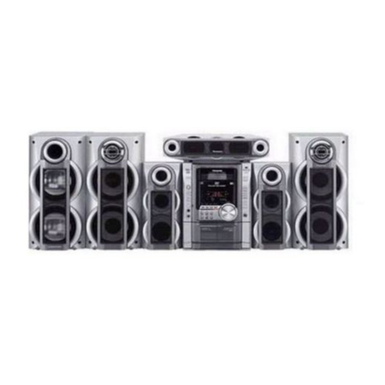
DVD Stereo System
SA-VK81DEE
Colour
(S)... Silver Type
Phone jack
Terminal
Mic jack
Sensitivity
Terminal
n CASSETTE DECK SECTION
Type
Track system
Head Record / Playback
Erasure
Motor
Recording System
Erase System
Tape Speed
Overall Frequency Response ( + 3, -6 dB) at DECK OUT
Normal (TYPE I)
S / N Ratio
Wow and Flutter
Fast Forward and Rewind Time
n DISC SECTION
Disc played [8 cm or 12 cm]
(1) DVD-RAM (DVD-VR compatible, JPEG formatted disc)
(2) DVD-Audio
(3) DVD-Video
(4) DVD-R (DVD-Video compatible)
© 2004 Panasonic AVC Networks Singapore Pte.
Ltd. (RCB Registration Number: 197701580H) All
rights
reserved.
distribution is a violation of law.
ORDER NO. MD0409420C3
Stereo, 3.5 mm jack
0.7 mV, 600 Ω
Mono, 6.3 mm jack (2 system)
Auto Reverse
4 Track, 2 Channel
Solid Permalloy Head
Double Gap Ferrite Head
DC Servo Motor
AC Bias 100 kHz
AC Erase 100 kHz
4.8 cm / s
35 Hz - 14 kHz
50 dB (A weighted)
0.18 % (WRMS)
Approx. 120 seconds with
C-60 cassette tape
Unauthorized
copying
and
Advertisement
Table of Contents

Related Manuals for Panasonic SA-VK81DEE


Summary of Contents for Panasonic SA-VK81DEE
-
Page 1: Specifications
(2) DVD-Audio Audio performance (Amplifier) (3) DVD-Video Input sensitivity / Input impedance (4) DVD-R (DVD-Video compatible) 250 mV, 20 k Ω © 2004 Panasonic AVC Networks Singapore Pte. Ltd. (RCB Registration Number: 197701580H) All rights reserved. Unauthorized copying distribution is a violation of law. -
Page 2: Table Of Contents
SA-VK81DEE (5) CD-Audio (CD-DA) Component video output (480P / 480I) 1 Vp-p (75 Ω ) (6) Video CD Y output level 0.7 Vp-p (75 Ω ) (7) SVCD (Conforming to IEC62107) output level 0.7 Vp-p (75 Ω ) (8) CD-R / CD-RW (CD-DA, Video CD, SVCD, MP3, WMA, JPEG... -
Page 3: Before Repair And Adjustment
SA-VK81DEE 11.4. Outline of the HighMAT standard 17.2. Checking the Main P.C.B., Power P.C.B., Power Supply 12 Procedure for repairing the set P.C.B., Power Amp P.C.B., Transformer P.C.B. and AC 12.1. Distinguish the problem Inlet P.C.B. 12.2. Diagnosis of Optical Pick-up Unit 17.3. -
Page 4: Protection Circuitry
SA-VK81DEE 2 Protection Circuitry The protection circuitry may have operated if either of the following conditions are noticed: · No sound is heard when the power is turned on. · Sound stops during a performance. The function of this circuitry is to prevent circuitry damage if, for example, the positive and negative speaker connection wires are “shorted”, or if speaker systems with an impedance less than the indicated rated impedance of the amplifier are used. -
Page 5: Prevention Of Electro Static Discharge (Esd) To
SA-VK81DEE 4 Prevention of Electro Static Discharge (ESD) to Electrostatically Sensitive (ES) Devices Some semiconductor (solid state) devices can be damaged easily by electricity. Such components commonly are called Electrostatically Sensitive (ES) Devices. Examples of typical ES devices are integrated circuits and some field-effect transistorsand semiconductor “chip”... -
Page 6: Cautions To Be Taken When Handling Optical Pickup
SA-VK81DEE 6 Cautions to be taken when handling Optical Pickup The laser diode used inside optical pickup could be destroyed due to static electricity as a potential difference is caused by electrostatic load discharged from clothes or human body. Handling the parts carefully to avoid electrostatic destructionduring repair. -
Page 7: Precaution Of Laser Diode
SA-VK81DEE 7 Precaution of Laser Diode Caution : This product utilizes a laser diode with the unit turned "ON", invisible laser radiation is emitted from the pick up lens. Wavelength : 662 nm(DVD)/785 nm(CD) Maximum output radiation power from pick up : 100 µW/VDE Laser radiation from pick up unit is safety level, but be sure the followings: 1. -
Page 8: Accessories
SA-VK81DEE 8 Accessories Remote control AC cord FM antenna AM antenna Video cable... -
Page 9: Operation Procedures
SA-VK81DEE 9 Operation Procedures... - Page 10 SA-VK81DEE...
-
Page 11: Disc Information
SA-VK81DEE 10 Disc information... - Page 12 SA-VK81DEE...
-
Page 13: About Highmat
SA-VK81DEE 11 About HighMAT 11.1. What is HighMAT? This word combines the abbreviations of Matsushita Electric Industrial Co. Ltd. and High Performance Media Access Technology, and is a trademark of Microsoft Corporation. The products with the HighMAT logo shown below are made according to the HighMATstandard. -
Page 14: Outline Of The Highmat Standard
SA-VK81DEE · You can also play digital content on the disc, which was created in accordance with the HighMAT format with a conventional CD-ROM player. 11.4. Outline of the HighMAT standard 1. Recording medium · CD-R/CD-RW · Supports ISO 9660 Level Expanded Joliet ·... - Page 15 SA-VK81DEE · WMA, MP3 (MPEG-1 Audio Layer 3) 64 kbps - 160.999 kbps, 44.1 KHz, stereo, fixed bit rate/ variable bit rate. · WMA, V2 and above, excluding Lossless/Voice/Pro · JPEG: Max 6M pixel, Maximum file size: 3 MB 4. Limitations regarding the number of files on the media, etc.
-
Page 16: Procedure For Repairing The Set
SA-VK81DEE 12 Procedure for repairing the set... -
Page 17: Distinguish The Problem
SA-VK81DEE 12.1. Distinguish the problem How to distinguish the trouble 1. View mechanical part if visual damage occurred. Confirm the movement of mechanical parts assembly (tray ass’y, loading mechanism ass’y, etc.). 2. Diagnose if Optical Pickup Unit is faulty (refer to diagnosis of Optical Pickup Unit). -
Page 18: Power Supply
SA-VK81DEE Checking Points Possible Faults Possible Reasons Countermeasure · Transformer output · Replace of Transformer T501 if found faulty. Transformer Circuit 1. No power supply voltage. voltage to the Power · Replace of Power Relay if found faulty. Circuit from AC In. - Page 19 SA-VK81DEE Terminal Defination (IC2809 - C9ZB00000377) Pin No Pin Name Pin Description 21/22 PYOUT1/PYOUT2 Signal Output Terminal for luminance signal (progressive type) 17/19 CrOUT/CbOUT Signal Output Terminal for color-difference signal COUT Signal Output Terminal for chroma signal 29/30 MIXOUT1/MIXOUT2 Signal Ouptut Terminal for Y/C Mix Signal...
-
Page 20: Diagnosis Of Optical Pick-Up Unit
SA-VK81DEE 12.2. Diagnosis of Optical Pick-up Unit How to distinguish Laser destruction/damage Confirmation 1 Remove cover of mechanism block so that you will see the lens of optical pickup. Confirm emission of laser at the moment when power switch is turned on. - Page 21 SA-VK81DEE While press and hold “STOP” on main unit , press “Display” button on the remote controller. Unit display laser current on FL. From the reading of display, you can judge if laser diode is damaged or not. Reading on the right side should be less than 70. If reading is more than 70, laser is damaged.
-
Page 22: Optical Pickup Self-Diagnosis And Replacement Procedure
SA-VK81DEE 13 Optical Pickup Self-Diagnosis and Replacement Procedure 13.1. Self-diagnosis This unit is equipped with the optical pickup self-diagnosis function and the tilt adjustment check function. Follow the procedure described below during repair in order to perform self-diagnosis and tilt adjustment effectively. Especially when “NODISC” is displayed, be sure to apply the self-diagnosis function before replacing with an optical pickup. -
Page 23: Cautions To Be Taken During Replacement Of Optical Pickup And Spindle Motor
SA-VK81DEE 13.2. Cautions to Be Taken During Replacement of Optical Pickup and Spindle Motor Before replacing the optical pickup and spindle motor, check a total usage time respectively. Follow the checking method described below. Item Status and Key Function Display... -
Page 24: Self-Diagnosis Function
SA-VK81DEE 14 Self-Diagnosis Function This unit is equipped with the self-diagnosis function, which displays an error when it occurs, for use during servicing. 14.1. Automatic Displayed Error Codes 14.1.1. Automatic Display Function For a power unit error, the code is automatically displayed. -
Page 25: Dvd / Cd Self-Diagnosis Error Code Description
SA-VK81DEE 14.4. DVD / CD Self-Diagnosis Error Code Description Error Code State, Conditon Cause, Troubleshooting The disc tray cannot be opened: it closes spontaneously. Disc tray open/close detection switch (S1001) failure. (Check and replace) The disc tray cannot be closed: it opens spontaneously. - Page 26 SA-VK81DEE Item Operational Details Display TO Exit Mode Condition and Key Function Jitter display While the player is Jitter display _yyy Press the STOP or stopped and no disc is Measures displays jitter. OPEN button. inserted, press Measurement repeated every...
- Page 27 SA-VK81DEE Item Operational Details Display TO Exit Mode Condition and Key Function Measurement of CD While the player is Measurement of CD laser current _032 _032 Automatically exits laser current electricity stopped and no disc is electricity the mode after five...
-
Page 28: Tray Lock Function
SA-VK81DEE Item Operational Details Display TO Exit Mode Condition and Key Function User reset While the player is Reset the unit. “DVD RESET” Automatically exits stopped and no disc is the mode after five inserted, press “STOP” seconds. & “ENTER” on remote control. -
Page 29: Cautions To Be Taken During Servicing
SA-VK81DEE Note: It is prohibited to unplug the power cable while the tray is opened and to close the tray manually. 15 Cautions To Be Taken During Servicing 15.1. Recovery after the dvd player is repaired · When Flash ROM or module(2) P.C.B. is replaced, carry out the recovery processing to optimize the drive. Playback the recovery disc to process the recovery automatically. -
Page 30: Total Usage Time Display
SA-VK81DEE 3. Select version upgrade process using the cursor keys on the remote controller unit. (Select YES or NO) 4. a. If YES is selected, the process starts. b. If NO is selected, only the recovery process is applied. 5. a. When the version upgrade process is complete, a message of completion appears on the screen. Remove the disc. -
Page 31: Disassembly And Assembly Of Main Component
SA-VK81DEE 16 Disassembly and Assembly of Main Component 16.1. Disassembly flow chart The following chart is the procedure for disassembling the casing and inside parts for internal inspection when carrying out the servicing. To assemble the unit, reverse the steps shown in the chart as below. -
Page 32: Disassembly Of Top Cabinet
SA-VK81DEE 16.2. Disassembly of Top Cabinet Step 1 Remove 3 screws each side and 5 screws at rear panel. Step 2 Lift up both sides of cabinet ass’y, push the cabinet ass’y toward the rear and remove the top cabinet. - Page 33 SA-VK81DEE Step 1 Disconnect FFC board (CN2811 , CN2815 & CN5806). Step 2 Lay the unit as shown below. Step 5 Remove 7 screws. Step 6 Detach FFC board (CP6803 & CP6800). Step 3 Remove 2 screws at the bottom chassis.
-
Page 34: P.c.b
SA-VK81DEE Step 11 Disconnect connector W601B. Step 12 Remove 5 screws. Step 13 Draw Tact Switch P.C.B. forward. 16.4.1. Disassembly of Lid · Follow the (Step 1) - (Step 2) of Item 16.2. · Follow the (Step 1) - (Step 7) of Item 16.3. - Page 35 SA-VK81DEE Step 2 Detach cables (CN5802 & CN5803). Step 4 Detach FFC boards (CN2811, CN2814 & CN2815). Step 3 Remove the 2 screws. Step 5 Lift up Main P.C.B. as arrow shown. 16.5.2. Disassembly of Power P.C.B. 16.5.1. Disassembly of Power Amp P.C.B.
- Page 36 SA-VK81DEE Step 3 Lift up Power P.C.B. as arrow shown. Step 2 Remove 2 screws fixed to the Power Amplifier IC 16.5.3. Disassembly of Power Supply and Voltage Regulator. P.C.B. Step 3 Break the joint with a metal cutter as shown below.
-
Page 37: Replacement For Traverse Deck
SA-VK81DEE Step 5 Fix back the bottom chasis with a screw as shown. NOTE: Insulate Power P.C.B. with insulation material to avoid short circuit. 16.5.4. Disassembly of Transformer P.C.B. · Follow the (Step 1) - (Step 2) of Item 16.2. - Page 38 SA-VK81DEE be careful not to lose them. Step 6 Remove the dvd module board and turn it over. Step 7 Pull FFC out from the connector. Note: Insert a short pin into FFC of the optical pickup. [See “Notice on handling of the optical pickup”].
- Page 39 SA-VK81DEE Step 10 Remove the catch of the drive rack, and take out the drive rack. Step 11 Place the convex part of an optical pickup to the concave part of a traverse base, then take out the optical pickup.
-
Page 40: Procedure For Removing Cd Loading Mechanism
SA-VK81DEE 16.8. Procedure for removing CD loading mechanism 1. Turn off by pressing power SW in the body. 3. Disassemble body, take out CD loading mechanism. 2. Unplug AC power cord after the indication of [GOOD-BYE], then disassemble the body. - Page 41 SA-VK81DEE...
- Page 42 SA-VK81DEE 16.9.3. Replacement for the traverse deck · Follow the (Step 1) - (Step 10) of item 16.9.2.
- Page 43 SA-VK81DEE 16.9.4. Disassembly for CD loading unit · Follow the (Step 1) - (Step 10) of item 16.9.2. · Follow the (Step 1) - (Step 3) of item 16.9.3.
- Page 44 SA-VK81DEE...
- Page 45 SA-VK81DEE...
-
Page 46: Cr16 Mechanism Assembly Procedure
SA-VK81DEE 16.10. CR16 MECHANISM ASSEMBLY PROCEDURE The following specified greases and/or oil must be applied when some specific parts are changed. 1. Floil grease (VFK1298) : The floil grease must be applied to tray, tray (L) and tray (R). 2. Hanarl oil (VFK1700) : The hanarl oil must be applied to... - Page 47 SA-VK81DEE...
- Page 48 SA-VK81DEE...
- Page 49 SA-VK81DEE...
- Page 50 SA-VK81DEE...
- Page 51 SA-VK81DEE...
- Page 52 SA-VK81DEE...
- Page 53 SA-VK81DEE...
- Page 54 SA-VK81DEE...
- Page 55 SA-VK81DEE...
- Page 56 SA-VK81DEE...
-
Page 57: Disassembly For Traverse Unit
SA-VK81DEE 16.11. Disassembly for Traverse Unit · Follow the (Step 1) - (Step 10) of item 16.9 · Follow the (Step 1) - (Step 3) of item 16.10... - Page 58 SA-VK81DEE...
-
Page 59: Disassembly Of Deck Mechanism Unit
SA-VK81DEE 16.12. Disassembly of Deck Mechanism Unit · Follow the (Step 1) - (Step 2) of Item 16.2. Step 6 Push the lever upward, and then open the cassette lid ass’y (For DECK1 and DECK2). · Follow the (Step 1) - (Step 7) of Item 16.3. - Page 60 SA-VK81DEE · Disassembly of pinch roller ass’y & head block Step 10 Remove 4 screws. Step 11 Remove Deck P.C.B. Step 12 Release the 2 claws, and then remove the pinch roller (R), (F). * The mechanism as shown below is for DECK1. For the one of DECK 2, perform the same procedures.
- Page 61 SA-VK81DEE Step 5 Remove the flywheel R. Step 6 Release the claw of tape side, and then remove the winding lever and spring. Step 7 Remove the flywheel F. [Installation of the belt] Step 1 The boss and marking should be positioned Step 2 Put the winding belt on the pulley temporarily.
- Page 62 SA-VK81DEE Step 7 Put the capstan belt A temporarily as shown below. Step 10 Remove 3 screws. Step 11 Put the capstan belt B as shown below. Step 8 Put the capstan belt B on the motor ass’y pulley. Step 12 Put the capstan belt A on the motor ass’y pulley.
-
Page 63: Replacement For The Cassette Lid Ass ' Y
SA-VK81DEE 16.13. Replacement for the cassette 16.14. Counter-measure for tape lid ass ’ y trouble · Follow the (Step 1) - (Step 2) of Item 16.2. · Follow the (Step 1) - (Step 2) of Item 16.2. Step 1 Force the lever upward, open the cassette lid ass’y. (For... -
Page 64: Service Position
SA-VK81DEE 17 Service Position 17.1. Checking Procedure Note: For the disassembling procedure, see Section 16. 17.2. Checking the Main P.C.B., Power P.C.B., Power Supply P.C.B., Power Amp P.C.B., Transformer P.C.B. and AC Inlet P.C.B. 1. Remove Top Cabinet and Rear Panel. -
Page 65: Checking The Panel P.c.b., Tact Switch P.c.b., Mic
SA-VK81DEE 17.3. Checking the Panel P.C.B., Tact Switch P.C.B., Mic P.C.B., Deck P.C.B. & Deck Mechanism P.C.B. 1. Remove Top Cabinet and Rear Panel. 2. Remove DVD Mechanism Unit. 3. Remove volume knob at front panel. 4. Remove Panel P.C.B., Mic P.C.B. & Tact Switch P.C.B. -
Page 66: Measurements And Adjustments
SA-VK81DEE 18 Measurements and Adjustments 18.1. Cassette Deck Section 18.1.2. Tape Speed Adjustment (Deck 1 / · Measurement Condition − − − − Reverse-mode selector switch: 1. Set the tape edit button to “NORMAL” position. − − − − Tape edit: NORMAL 2. -
Page 67: Tuner Section
SA-VK81DEE 18.1.4. Bias Frequency Adjustment (Deck 1 / 2) 1. Set the unit to “AUX” position. 2. Insert the Normal blank tape (QZZCRA) into DECK 2 and set the unit to “REC” mode (l use “REC/STOP” key). 3. Adjust L1002 so that the output frequency is within the standard value. -
Page 68: Alignment Points
SA-VK81DEE 18.3. Alignment Points 18.3.1. Cassette Deck Section 18.3.2. Adjustment Point... -
Page 69: Block Diagram
SA-VK81DEE 19 Block Diagram OPTICAL PICK UP UNIT ACTUATOR FOCUS TRACKING TURNTABLE COIL COIL IC8251 IC8271 LDIN, 24~26 BIAS2, C0GBG0000044 C0GBF0000004 TRIN MOTOR DRIVE IC MOTOR DRIVE IC IC8001 MN2DS0003APH DV2.1 LSI 1,2,4,5,7,8, 217,220, 249,251 234,232 248,245, 221,223,224, 244,240 10,11,13~15,... - Page 70 SA-VK81DEE OPTICAL PICKUP UNIT HIGH FREQUENCY DVD MODULATOR CD MODULATOR MODULATOR QR8571 SWITCH (SUPPLY CONTROL) Q8552 Q8562 SWITCH SWITCH Q8551 Q8561 SWITCH SWITCH IC8001 MN2DS0003APH DV2.1 LSI IC8611 C3EBGC000056 EEPROM IC (NOT SUPPLIED)
-
Page 71: Power Supply
SA-VK81DEE TO MAIN BLOCK Q2810 INVERTER SWITCH 16(20) 14(13) 12(11) JK2801 S-VIDEO C OUT IC8451 Y OUT1 ZFLGA C0FBBK000036 A/D CONVERTER Y OUT2 IC2809 C9ZB00000377 VIDEO BUFFER IC8111 CR OUT C0CBCBD00018 POWER SUPPLY IC CB OUT JK2802 PY OUT1 PY OUT2... - Page 72 SA-VK81DEE IC1001 AN7348S-E1 P.B. EQ/REC AMP/ ALC/TPS AMP 24(23) (DECK 1) Q1014(Q1015) P.B. HEAD 1(2) 20(5) BUFFER 22(3) 21(4) 17(8) (DECK 2) 18(7) R/P HEAD NOR/CrO & HI/LO LOGIC Q1012 Q1020 LOGIC L/H (Q1013) (Q1021) MUTING MUTING SWITCH RIPPLE LOGIC...
- Page 73 SA-VK81DEE 72(73) EXIN1(2) 7(8) INL(R)_SB 61(62) INA1(2) IN_C OUTC IC2812 KIA4558FEL DUAL OP-AMP FOUT1 IC2815 C1BB00000845 ASP IC 39(36) OUTFL(R) 63(64) 40(37) INB1(2) FIN4(3) JK2803 LINE 25(23) OUTLS(R) 67(68) 75(76) 78(79) 65(66) 59(60) 41(38) Q2813 MUTING SWITCH Q2814 MUTING SWITCH...
- Page 74 SA-VK81DEE 2(6) 1(7) IC2811 C0AABB000117 HP AMP 7(1) 5(3) IC2819 KIA4558FEL DUAL OP-AMP Q2841, Q2842 SWITCH IC2817 IC2818 C0ABCB000052 C0JBAR000292 QUAD OP-AMP ANALOG SWITCH IC2816 1(3) 15(4) C0ABCB000052 QUAD OP-AMP 2(5) Q2820 MUTING SWITCH Q6813 Q6814 Q2839 SWITCH SWITCH SWITCH...
- Page 75 SA-VK81DEE VR6801 Q6806,Q6807 Q6817 LIMITER JK6800 MIC1 IC2813 C1BB00000801 KARAOKE IC JK6802 MIC2 64(63) 75(74) S6810~S6815 KEY SW FL6800 FROM POWER FL DISPLAY TRANSFORMER Q6825~ Q6828 RM11 RM21 UP/DOWN MOTOR LOADING MOTOR DRIVER 62~64, 51~25, 23~18 IC6803 IC11 IC21 58~61...
- Page 76 SA-VK81DEE L2802 IC2807 IC2802 C0DBEFG00003 FR_L(R) REGULATOR C0DBAZG00033 DC TO DC CONVERTER FILTER FILTER FILTER L2805 FILTER IC2803 C0DBAZG00033 DC TO DC CONVERTER FILTER SUBWOOFER D2835 LR IN LR OUT CENTER C OUT C OUT IC2801,IC2806 1(2) 26(25) SURRL(R) C0CBADG00005...
-
Page 77: Power Supply
SA-VK81DEE 3(6) 21(20) L OUT(R) L IN(R) JK5803 (JK5804) D5854(D5859) D5855 JK5803 IC5803 D5821 CENTER RSN312H24-P Q5810~ POWER HIC Q5812 D5856 SWITCH JK5804 SUBWOOFER Q5809 SWITCH Q5805,Q5806 D5819(D5820) REGULATOR Q5807, Q5808 D5823 -VCC LOW REGULATOR AC IN -Di SENS D5822... -
Page 78: Schematic Diagram
SA-VK81DEE 20 Schematic Diagram (All schematic diagrams may be modified at any time with the Secondary trouble can be prevented by taking care during development of the new technology) repair. · Cover the parts boxes made of plastics with aluminium foil. -
Page 79: Optical Pickup Unit Circuit
SA-VK81DEE 20.1. Optical Pickup Unit Circuit SCHEMATIC DIAGRAM - 1 OPTICAL PICKUP UNIT CIRCUIT : +B SIGNAL LINE : CD-DA SIGNAL LINE J0JBC0000105 TO ACT J0JBC0000105 GND (IM) MODULE VREF2(RF-) (IN/OUT) CIRCUIT PIN (DVD) (FP8501) ON LD (CD) SCHEMATIC LD GND... -
Page 80: A) Dvd Module Circuit
SA-VK81DEE 20.2. (A) DVD Module Circuit SCHEMATIC DIAGRAM - 2 DVD MODULE (IN/OUT) CIRCUIT : +B SIGNAL LINE : CD-DA SIGNAL LINE IC8271 C0GBF0000004 MOTOR DRIVE IC IC8271 C8275 FP8271 TC8271 COIL_W CP8273 TC8272 COIL_V C8284 0.01 TC8273 COIL_U CP8272... -
Page 81: Power Supply
SA-VK81DEE SCHEMATIC DIAGRAM - 3 : DVD AUDIO SIGNAL LINE DVD MODULE (IN/OUT) CIRCUIT : +B SIGNAL LINE : CD-DA SIGNAL LINE R8271 CP8423 DMIXOUT 0.39 SBI3 SBO3 SBT3 RA8271 STBDAC (10K x 2) MUTE3 SPDRV PNRST ADAC-CLK R8451 CP8421... - Page 82 SA-VK81DEE SCHEMATIC DIAGRAM - 4 : MAIN SIGNAL LINE : DVD AUDIO SIGNAL LINE DVD MODULE (IN/OUT) CIRCUIT : +B SIGNAL LINE : DVD VIDEO SIGNAL LINE C8423 C8424 C8451 C8452 C8420 6.3V330 FP8101 VGND Y/PY/G LB8303 J0JCC0000119 TC8303 Y/PY/G...
- Page 83 SA-VK81DEE SCHEMATIC DIAGRAM - 5 DVD MODULE (DV2) CIRCUIT : +B SIGNAL LINE IC8651 RFKFMH81T161 FLASH ROM IC EXADT15 EXADR16 EXADT14 XBYTE EXADT13 EXADT12 FDT15 DQ15/A-1 EXADT11 FDT7 EXADT10 FDT14 DQ14 EXADT9 FDT6 EXADT8 FDT13 DQ13 EXADR19 FDT5 EXADR20 FDT12...
- Page 84 SA-VK81DEE SCHEMATIC DIAGRAM - 6 DVD MODULE (DV2) CIRCUIT : +B SIGNAL LINE IC8051 C8028 C8026 C8027 C8024 C8023 6.3V1 6.3V1 2200P 6.3V1 C3ABPG000133 64MB SDRAM IC C8051 6.3V1 MDQ0 MDQ15 DQ15 C8052 VDDQ VSSQ C8022 C8025 MDQ1 MDQ14 DQ14...
- Page 85 SA-VK81DEE SCHEMATIC DIAGRAM - 7 DVD MODULE (DV2) CIRCUIT : +B SIGNAL LINE RA8018 (82 x 4) RA8017 RA8014 (82 x 4) C8021 (82 x 4) RA8015 (22 x 2) MDQ9 MDQ24 MDQ5 VDD33 MDQ10 TRCST MDQ4 TRCDATA3 VDD33 TRCDATA2...
- Page 86 SA-VK81DEE SCHEMATIC DIAGRAM - 8 : CD-DA SIGNAL LINE : DVD VIDEO SIGNAL LINE DVD MODULE (DV2) CIRCUIT : +B SIGNAL LINE : DVD AUDIO SIGNAL LINE LB8001 J0JHC0000045 D+3.3V D+1.2V C8002 C8001 LB8002 330P 100P J0JHC0000045 RA8031 C8017 (4.7K x 2) RA8032 (4.7K x 2)
-
Page 87: B) Main Circuit
SA-VK81DEE 20.3. (B) Main Circuit SCHEMATIC DIAGRAM - 9 : MIC SIGNAL LINE : MAIN SIGNAL LINE : +B SIGNAL LINE : AUX SIGNAL LINE : PLAYBACK SIGNAL LINE MAIN CIRCUIT : -B SIGNAL LINE : AM/FM SIGNAL LINE : RECORD SIGNAL LINE... - Page 88 SA-VK81DEE SCHEMATIC DIAGRAM - 10 : +B SIGNAL LINE MAIN CIRCUIT : -B SIGNAL LINE : MAIN SIGNAL LINE C2144 R2158 R2157 50V47 3.3K C2142 LINE_LIN KA_LOUT LINE_RIN R2155 C2140 50V4.7 EXT_R C2141 R2156 R2159 C2143 50V33 100K 0.01 IC2819...
- Page 89 SA-VK81DEE SCHEMATIC DIAGRAM - 11 : MIC SIGNAL LINE MAIN CIRCUIT : +B SIGNAL LINE : MAIN SIGNAL LINE +7.5V CD8V LOAD_GND R2978 CHANGE_SW CHANGE_SW KA_ROUT KA_LOUT UP/DOWN_F R2979 UP/DOWN_F KA_RIN C2218 16V10 UP/DOWN_R R2980 UP/DOWN_R CD LOADING KA_LIN C2120...
- Page 90 SA-VK81DEE SCHEMATIC DIAGRAM - 12 : MAIN SIGNAL LINE : +B SIGNAL LINE : AUX SIGNAL LINE : PLAYBACK SIGNAL LINE MAIN CIRCUIT : -B SIGNAL LINE : AM/FM SIGNAL LINE : RECORD SIGNAL LINE R2146 R2245 8.2K 8.2K SURR_C...
- Page 91 SA-VK81DEE SCHEMATIC DIAGRAM - 13 : +B SIGNAL LINE MAIN CIRCUIT : -B SIGNAL LINE : MAIN SIGNAL LINE Q2815, 2816 B1GDCFGA0014 R2871 R2881 MUTING SWITCH Q2815 Q2816 Q2825 B1ABEB000001 MUTING SWITCH R2870 R2872 R2959 220K R2868 R2869 C2860 R2873...
-
Page 92: Power Supply
SA-VK81DEE SCHEMATIC DIAGRAM - 14 : +B SIGNAL LINE MAIN CIRCUIT : -B SIGNAL LINE : MAIN SIGNAL LINE R2220 +15V +15V FR_L FR_R AGND POWER SUPPLY R2996 AGND IC2812 CIRCUIT LSURR R2324 (CP5801) ON KIA4558FEL R2412 RSURR SCHEMATIC DUAL OP-AMP IC... -
Page 93: Power Supply
SA-VK81DEE SCHEMATIC DIAGRAM - 15 : DVD VIDEO SIGNAL LINE MAIN CIRCUIT : +B SIGNAL LINE : MAIN SIGNAL LINE DVD_STA DVD_STA DVD_CMD DVD_CMD DVD_CLK DVD_CLK MGND M+9V D2836 MGND B0EAKM000117 M+9V MOT10V DGND D+1.2V AGND D+1.2V D+1.2V AGND A+5V... - Page 94 SA-VK81DEE SCHEMATIC DIAGRAM - 16 : +B SIGNAL LINE MAIN CIRCUIT : -B SIGNAL LINE Q2838 B1GBCFJA0015 SWITCH C2952 50V4.7 D2831, 2833 B0ACCK000005 R2993 C2804 R2972 C2820 6.3V220 R2809 4.7K L2805 G0A101G00022 IC2806 IC2801 IC2806 IC2801 IC2803 C0CBADG00005 C0CBADG00005 C0DBAZG00033...
- Page 95 SA-VK81DEE SCHEMATIC DIAGRAM - 17 : +B SIGNAL LINE MAIN CIRCUIT : -B SIGNAL LINE DCDET R2913 Q2831 B1ABCF000011 C2871 DCDET SWITCH 16V330 D2826 B0ACCK000005 Q2830 R2895 R2638 Q2830 100K B1ADCF000001 CN2806 FAN MOTOR DRIVE R2894 D2825 D2824 D2824, 2825...
-
Page 96: C) Panel Circuit , (D) Mic Circuit & (E) Tact Switch Circuit
SA-VK81DEE 20.4. (C) Panel Circuit , (D) Mic Circuit & (E) Tact Switch Circuit SCHEMATIC DIAGRAM - 18 : +B SIGNAL LINE : TAPE PLAYBACK SIGNAL LINE PANEL CIRCUIT : -B SIGNAL LINE : TAPE RECORD SIGNAL LINE : MIC SIGNAL LINE... -
Page 97: Panel Circuit
SA-VK81DEE SCHEMATIC DIAGRAM - 19 : +B SIGNAL LINE PANEL CIRCUIT : -B SIGNAL LINE : MAIN SIGNAL LINE R6108 Q6825 - 6828 100K B1ABCF000131 R6107 Q6828 SWITCH 100K Q6827 R6106 100K Q6826 R6105 Q6825 100K R6872 R6878 R6876 R6874 C6893 6.3V100... - Page 98 SA-VK81DEE SCHEMATIC DIAGRAM - 20 : +B SIGNAL LINE PANEL CIRCUIT : -B SIGNAL LINE FL6800 A2BD00000092 FL DRIVER 54 53 52 51 50 49 48 47 46 45 44 43 42 41 40 39 38 37 36 35 34 33 32 31 30 29 28 27 26 25 24 23 22 21 20 19 18 17 16 15 14 13 12 11 10 9 8 7 6 5 4 3...
- Page 99 SA-VK81DEE SCHEMATIC DIAGRAM - 21 : +B SIGNAL LINE : TAPE PLAYBACK SIGNAL LINE : MAIN SIGNAL LINE PANEL CIRCUIT : -B SIGNAL LINE : TAPE RECORD SIGNAL LINE : MIC SIGNAL LINE SYNC SYNC SYS6V SYS6V POWER PCONT PCONT...
-
Page 100: F) Deck Circuit & (G) Deck Mechanism Circuit
SA-VK81DEE 20.5. (F) Deck Circuit & (G) Deck Mechanism Circuit SCHEMATIC DIAGRAM - 22 : +B SIGNAL LINE : RECORD SIGNAL LINE DECK CIRCUIT : PLAYBACK SIGNAL LINE R1055 C1038 R1020 R1098 2.2K 220P R1100 R1101 C1034 C1044 R1015 50V3.3... - Page 101 SA-VK81DEE SCHEMATIC DIAGRAM - 23 PANEL CIRCUIT : +B SIGNAL LINE (CP6803) ON SCHEMATIC : RECORD SIGNAL LINE DIAGRAM - 18 DECK CIRCUIT : PLAYBACK SIGNAL LINE CN1001 R1002 C1054 50V3.3 R1060 C1064 50V3.3 R1095 R1091 Q1017 100K 2.2K R1057...
-
Page 102: H) Power Supply Circuit
SA-VK81DEE 20.6. (H) Power Supply Circuit SCHEMATIC DIAGRAM - 24 : +B SIGNAL LINE POWER SUPPLY CIRCUIT : -B SIGNAL LINE : MAIN SIGNAL LINE IC5801 RSN309W44B POWER HIC 5801 5802 5803 5804 C5400 820P R5602 C5803 C5300 C5500 0.01... -
Page 103: Power Supply
SA-VK81DEE SCHEMATIC DIAGRAM - 25 : +B SIGNAL LINE POWER SUPPLY CIRCUIT : -B SIGNAL LINE : MAIN SIGNAL LINE Q5803 Q5812 B1AAGC000007 B1AACF000089 Q5812 MUTING SWITCH SWITCH R5842 R5817 R5843 Q5803 100K D5803 - 5806 C5823 B0BA01900005 50V2.2 D5803... -
Page 104: I) Power Amp Circuit
SA-VK81DEE 20.7. (I) Power Amp Circuit SCHEMATIC DIAGRAM - 26 : +B SIGNAL LINE POWER AMP CIRCUIT : -B SIGNAL LINE : MAIN SIGNAL LINE IC5803 RSN312H24-P POWER AMP C5200 820P R5202 C5100 C5201 820P R5102 C5828 C5101 0.01 R5100... -
Page 105: J) Power Circuit
SA-VK81DEE 20.8. (J) Power Circuit SCHEMATIC DIAGRAM - 27 : +B SIGNAL LINE POWER CIRCUIT : -B SIGNAL LINE : MAIN SIGNAL LINE POWER SUPPLY CIRCUIT POWER SUPPLY CIRCUIT (CP5803) ON (H5801/W5801) ON SCHEMATIC DIAGRAM - 24 SCHEMATIC DIAGRAM - 25... - Page 106 SA-VK81DEE SCHEMATIC DIAGRAM - 28 : +B SIGNAL LINE POWER CIRCUIT : -B SIGNAL LINE : MAIN SIGNAL LINE POWER AMP CIRCUIT (H5803/W5803) ON SCHEMATIC DIAGRAM - 26 CN5807 1 2 3 4 5 6 D5832 D5831 D5846 D5847 B0FBAM000009...
-
Page 107: K) Transformer Circuit, (L) Ac Inlet Circuit & (M) Cd Loading Circuit
SA-VK81DEE 20.9. (K) Transformer Circuit, (L) AC Inlet Circuit & (M) CD Loading Circuit SCHEMATIC DIAGRAM - 29 TRANSFORMER CIRCUIT : +B SIGNAL LINE T501 G4C8AHK00003 CN950 P(0) S2’ P(110) POWER CIRCUIT S1’ (H5804/W5804) ON P(123) SCHEMATIC DIAGRAM - 28 S3’... -
Page 108: Printed Circuit Board
SA-VK81DEE 21 Printed Circuit Board 21.1. (A) DVD Module P.C.B. (Side: A & B ) DVD MODULE P.C.B (REP3654Q) C8503 LB8502 TP8517 TP8500 TC8501 TC8502 TP8511 TP8520 TP8515 LB8501 TP8516 TP8521 C8505 RA8502 TP8510 TP8502 TP8519 TP8501 IC8251 TP8524 C8502... - Page 109 SA-VK81DEE DVD MODULE P.C.B (REP3654Q) CP8252 C8254 C8255 FP8501 CP8251 C8251 C8252 R8251 Q8552 C8561 Q8562 R8554 C8550 R8566 C8554 R8567 IC8605 R8564 Q8606 R8553 R8558 R8563 R8565 Q8605 R8559 C8605 C8564 C8606 C8551 C8695 TC8006 R8605 R8606 IC8691 IC8695...
-
Page 110: B) Main P.c.b
SA-VK81DEE 21.2. (B) Main P.C.B. MAIN P.C.B R2817 CN2810 W2360 R2819 CN2813 (REPX0433A) L2809 C2831 C2830 W2295 R2984 W2294 R2986 C2828 R2843 W2296 W2184 C2825 IC2809 C2107 W2287 C2826 W2829 C2822 C2303 C2824 C2829 C2600 C2400 D2836 C2806 R2996 R2995... - Page 111 SA-VK81DEE Q2810 R2819 L2809 W2110 C2831 R2820 C2830 R2823 C2842 R2831 L2813 C2849 JK2802 C2828 R2830 C2825 IC2809 R2833 C2826 2-PR C2847 C2824 R2821 C2829 C2600 R2996 R2995 Q2832 C2500 C2837 5-PB C2846 W2116 CN2809 CN2806 W2107 Q2836 C2840 R2994...
-
Page 112: C) Panel P.c.b
SA-VK81DEE 21.3. (C) Panel P.C.B. PANEL P.C.B (REPX0434G) S6811 DISC_CHECK Z6800 SENSOR C6851 R6937 S6810 POWER W6237 FL6800 C6855 W6236 C6845 R6108 C6853 R6107 R6996 R6105 Q6820 R6106 S6812 MULTI D6815 RE-MASTER C6894 IC6801 W6205 C6888 C6887 C680 W6198 C6803... - Page 113 SA-VK81DEE S6816 CD OPEN/CLOSE S6817 DISC CHANGE S6819 DISC_5 D6804 C6856 R6965 S6820 W6256 DISC_4 R6900 W6105 C6858 R6929 W6131 R6966 S6821 DISC_3 C6804 C6859 C6803 W6203 W6129 IC6802 C6863 R6896 S6822 R6967 R6897 DISC_2 R6979 R6895 R6894 C6862 C6813...
-
Page 114: D) Mic P.c.b. & (E) Tact P.c.b
SA-VK81DEE 21.4. (D) Mic P.C.B. & (E) Tact P.C.B. MIC P.C.B (REPX0434G) VR6801 C6867 R6994 R6982 Q6806 Q6807 R6987 W6103 C6872 C6879 Q6817 R6891 C6869 R6892 L6809 W6102 C6875 C6881 C6871 L6806 L6807 C6876 TACT P.C.B (REPX0434G) VOLUME S6800 S6801... -
Page 115: F) Deck P.c.b. & (G) Deck Mechanism
SA-VK81DEE 21.5. (F) Deck P.C.B. & (G) Deck Mechanism DECK P.C.B. DECK MECHANISM P.C.B. (REPX0331C) (REPX0321B) Q1001 R1024 IC1004 C1006 R1006 C1009 R1027 C1003 Q1003 J1002 L1002 R1004 R1001 Q1007 J1003 W1002 C1026 C1011 S951 C1021 C1020 C1016 Q1004 Q1017... -
Page 116: H) Power Supply P.c.b
SA-VK81DEE 21.6. (H) Power Supply P.C.B. POWER SUPPLY P.C.B (REPX0432E) E5801 CP5803 CP5804 1 2 3 4 5 6 7 8 9 10 11 12 1 2 3 4 5 6 7 8 9 10 11 12 Q5802 C5819 D5860... -
Page 117: I) Power Amp P.c.b. & (M) Cd Loading P.c.b
SA-VK81DEE 21.7. (I) Power Amp P.C.B. & (M) CD Loading P.C.B. POWER AMP P.C.B(REPX0432E) IC5803 22 21 20 19 18 17 16 15 14 13 12 11 10 9 C5200 C5827 C5100 C5201 R5202 C5828 R5846 R5888 W5244 W5808 W5296... -
Page 118: J) Power P.c.b
SA-VK81DEE 21.8. (J) Power P.C.B. POWER P.C.B (REPX0432E) W5533 W5809 W5848 T6.3AL 250V T6.3AL 250V R5303 R5859 C5502 Q5816 C5503 Q5818 Q5815 R5889 R5857 C5402 L5001 W5144 R5858 C5848 W5302 W5407 R5890 H5805/W5805 L5002 W5317 R5205 C5846 C5847 C5205 R5105... - Page 119 SA-VK81DEE W5533 W5848 CN5807 R5859 Q5816 C5848 W5302 W5810 R5878 D5851 R5877 W5443 W5306 W5305 W5442 CN5806 W5351 W5249 R5818 W5350 W5441 W5402 W5403 R5876 W5440 W5248 W5139 W5504 14 13 12 11 W5503 CN5810 W5439 W5532 W5471 W5304 W5820...
-
Page 120: K) Transformer P.c.b
SA-VK81DEE 21.9. (K) Transformer P.C.B. TRANSFORMER P.C.B (REPX0431C) RL502 D950 CN951 CN950 (YEL) (BLK) T501(MAIN TRANSFORMER) SECONDARY PRIMARY CAUTION RISK OF ELECTRIC SHOCK AC VOLTAGE LINE. PLEASE DO NOT TOUCH THIS P.C.B... -
Page 121: L) Ac Inlet P.c.b
SA-VK81DEE 21.10. (L) AC Inlet P.C.B. AC INLET P.C.B (REPX0431C) (YEL) (BLK) F1 T4AL 250V CN953 T502 (SUB-TRANSFORMER) L500 J584 AC IN J585 230-240V 50Hz J586 J587 JK500 CAUTION RISK OF ELECTRIC SHOCK AC VOLTAGE LINE. PLEASE DO NOT TOUCH THIS P.C.B... -
Page 122: Wiring Connection Diagram
SA-VK81DEE 22 Wiring Connection Diagram SENSOR 1 ... . 26 PANEL P.C.B. SOLDER SIDE FP8501 H6806/ W6805 MIC 2 H6805/ W6805 JK6802 CP6802 27 ..1 13 . - Page 123 SA-VK81DEE DECK P.C.B. SOLDER SIDE CS1002 1. . . 5 MOTOR CN953 W1002 (DECK 2) R/P HEAD, ERASE HEAD AC INLET P.C.B. SOLDER SIDE CN971 L500 AC IN 230~240V 50HZ T502 JK500 SUB-TRANSFORMER CAUTION RISK OF ELECTRIC SHOCK AC VOLTAGE LINE.
-
Page 124: Illustration Of Ics, Transistors And Diodes
SA-VK81DEE 23 Illustration of ICs, Transistors and Diodes C0EBE0000384 RSN312H24-P C1BB0000086(18P) C0HBB0000039 (64P) C0EBA0000031 C5BA00000113 C9ZB00000377(32P) C0FBBK000036 (48P) C0JBAA000346 KIA4558FEL(8P) C1BB00000801 (80P) C3ABPG000063(54P) C1BB00000845 (80P) C0GBF0000004 (16P) C2CBJG000460 (100P) AN7348S-E1 (24P) MN2DS0003APH (256P) C0JBAR000292 (16p) RSN309W44B C0DBAZG00033 (5P) CNB13030R2AU C0ABCB000052 (14P) -
Page 125: Terminal Function Of Ic
SA-VK81DEE 24 Terminal Function of IC 24.1. IC6800 (C2CBJG000486) Pin No. Mark Function For Flash System Microprocessor FLD_RST Reset Signal for the FL Driver Pin No. Mark Function FLD_CS Latch Signal for the FL ST_SW Stock switch of changer Driver... -
Page 126: Power Supply
SA-VK81DEE Pin No. Mark Function DECK_AD1 Deck AD Input 1 (Mode 1/Half 1) DECK_AD2 Deck Input (RINHF/MODE2/RINH/HAL KEY3 Key 3 line input KEY2 Key 2 line input DES3 REGION Setting for DVD SPEANA_A/D A/DI Connect to Speana IC’s OUT port... -
Page 127: Parts Location And Replacement Parts List
SA-VK81DEE 25 Parts Location and Replacement Parts List Notes: · Important safety notice: Components identified by mark have special characteristics important for safety. Furthermore, special parts which have purposes of fire-retardent (resistors), high-quality sound (capacitors), low noise (resistors), etc are used. -
Page 128: Deck Mechanism (Raa3412-S)
SA-VK81DEE 25.1. Deck Mechanism (RAA3412-S) 25.1.1. Deck Mechanism Parts Location... - Page 129 SA-VK81DEE...
-
Page 130: Deck Mechanism Parts List
SA-VK81DEE 25.1.2. Deck Mechanism Parts List Ref. No. Part No. Part Name & Description Remarks CASSETTE DECK RED0071 R/P HEAD BLOCK UNIT RED0072 P/B HEAD BLOCK UNIT RDG0300 REEL BASE GEAR RDG0301 WINDING RELAY GEAR RDK0026 MAIN GEAR RDR0029-3 RELAY PULLEY... -
Page 131: Dvd Loading Mechanism
SA-VK81DEE 25.2. DVD Loading Mechanism 25.2.1. DVD Loading Mechanism Parts Location... - Page 132 SA-VK81DEE...
- Page 133 SA-VK81DEE...
- Page 134 SA-VK81DEE 25.2.2. DVD Loading Mechanism Parts List Ref. No. Part No. Part Name & Description Remarks Ref. No. Part No. Part Name & Description Remarks TRAVERSE DECK XTBS26+8J SCREW RAE2008W-S DT68 TRV SUB UNIT RDG0519 MAIN GEAR RMG0598-A FLOATING RUBBER...
-
Page 135: Cabinet
SA-VK81DEE 25.3. Cabinet 25.3.1. Cabinet Parts Location... - Page 136 SA-VK81DEE...
- Page 137 SA-VK81DEE...
-
Page 138: Electrical Parts List
SA-VK81DEE 25.3.2. Cabinet Parts List Ref. No. Part No. Part Name & Description Remarks Ref. No. Part No. Part Name & Description Remarks CABINET AND CHASSIS RKFX0124-1S CASS LID (R) RKMX0077E-S TOP CABINET (BENT) ENG07802QF TUNER PACK RKWX0236-H3 FL WINDOW... - Page 139 SA-VK81DEE Ref. No. Part No. Part Name & Description Remarks Ref. No. Part No. Part Name & Description Remarks Q2813 B1GFGCAA0001 TRANSISTOR Q6833 B1GBCFJJ0039 TRANSISTOR Q2814 B1GDCFGA0014 TRANSISTOR Q6834 B1GBCFJJ0039 TRANSISTOR Q2815 B1GDCFGA0014 TRANSISTOR Q6835 B1GBCFJJ0039 TRANSISTOR Q2816 B1GDCFGA0014 TRANSISTOR...
- Page 140 SA-VK81DEE Ref. No. Part No. Part Name & Description Remarks Ref. No. Part No. Part Name & Description Remarks D5833 B0EAKM000126 DIODE LB8693 ERJ3GEYJ101V 100 1/16W D5834 B0EAKM000126 DIODE D5835 B0BA02600018 DIODE VARIABLE RESISTORS D5836 B0EAKM000125 DIODE D5837 B0EAKM000125 DIODE...
- Page 141 SA-VK81DEE Ref. No. Part No. Part Name & Description Remarks Ref. No. Part No. Part Name & Description Remarks CN6800 K1KA11B00033 11P CONNECTOR RELAY CP5801 K1KA12A00184 12P CONNECTOR CP5802 K1KA12A00184 12P CONNECTOR RL502 K6B1AEA00003 MAGNET RELAYS CP5803 K1KA12A00184 12P CONNECTOR...
- Page 142 SA-VK81DEE Ref. No. Part No. Part Name & Description Remarks Ref. No. Part No. Part Name & Description Remarks W5803 REXX0302 8P FLAT WIRE R1095 ERJ3GEYJ104V 100K 1/16W W5804 REXX0297 10P FLAT WIRE R1096 ERJ3GEYJ104V 100K 1/16W W5805 REXX0296 7P FLAT WIRE...
- Page 143 SA-VK81DEE Ref. No. Part No. Part Name & Description Remarks Ref. No. Part No. Part Name & Description Remarks R2207 ERJ3GEY0R00V 0 1/16W R2325 ERJ3GEYJ563V 56K 1/16W R2208 ERJ3GEYJ104V 100K 1/16W R2335 ERJ3GEY0R00V 0 1/16W R2209 ERJ3GEYJ272V 2.7K 1/16W R2336...
- Page 144 SA-VK81DEE Ref. No. Part No. Part Name & Description Remarks Ref. No. Part No. Part Name & Description Remarks R2812 ERJ3GEYJ102V 1K 1/16W R2908 ERJ3GEYJ103V 10K 1/16W R2813 ERJ3GEYJ102V 1K 1/16W R2909 ERJ3GEYJ563V 56K 1/16W R2814 ERJ3GEYJ102V 1K 1/16W R2910...
- Page 145 SA-VK81DEE Ref. No. Part No. Part Name & Description Remarks Ref. No. Part No. Part Name & Description Remarks R5202 ERDS2TJ563T 56K 1/4W R5859 ERDS2TJ332T 3.3K 1/4W R5205 ERDS1FVJ100T 10 1/2W R5860 ERDS2TJ824T 820K 1/4W R5300 ERDS2TJ272T 2.7K 1/4W R5865...
- Page 146 SA-VK81DEE Ref. No. Part No. Part Name & Description Remarks Ref. No. Part No. Part Name & Description Remarks R6808 ERJ3GEYJ102V 1K 1/16W R6893 ERJ3GEYJ102V 1K 1/16W R6809 ERJ3GEYJ102V 1K 1/16W R6894 ERJ3GEYJ102V 1K 1/16W R6810 ERJ3GEYJ103V 10K 1/16W R6895...
- Page 147 SA-VK81DEE Ref. No. Part No. Part Name & Description Remarks Ref. No. Part No. Part Name & Description Remarks R6976 ERJ3GEYJ222V 2.2K 1/16W R8570 ERJ3GEYJ104V 100K 1/16W R6979 ERJ3GEYJ104V 100K 1/16W R8601 ERJ3GEYJ102V 1K 1/16W R6980 ERJ3GEYJ104V 100K 1/16W R8605...
- Page 148 SA-VK81DEE Ref. No. Part No. Part Name & Description Remarks Ref. No. Part No. Part Name & Description Remarks C1033 F1C1C183A001 0.018 16V C2211 ECEA1HKA4R7B 4.7 50V C1034 ECEA1HKA3R3B 3.3 50V C2213 ECJ1VC1H101K 100P 50V C1035 ECEA1HKA3R3B 3.3 50V C2214...
- Page 149 SA-VK81DEE Ref. No. Part No. Part Name & Description Remarks Ref. No. Part No. Part Name & Description Remarks C2609 ECEA1HKA100B 10 50V C2905 ECJ1VB1H102K 1000P 50V C2610 ECJ1VC1H102J 1000P 50V C2906 ECJ1VB1A224K 0.22 10V C2802 EEUFC0J821B 820P 6.3V C2907...
- Page 150 SA-VK81DEE Ref. No. Part No. Part Name & Description Remarks Ref. No. Part No. Part Name & Description Remarks C5502 F1D1H1040002 0.1 50V C6812 ECJ1VB1H102K 1000P 50V C5503 F1D1H1040002 0.1 50V C6813 ECJ1VC1H101K 100P 50V C5601 ECBT1H150JC5 15P 50V C6814...
-
Page 151: Packing Materials & Accessories Parts List
SA-VK81DEE Ref. No. Part No. Part Name & Description Remarks Ref. No. Part No. Part Name & Description Remarks C6898 ECJ1VB1H102K 1000P 50V C8233 ECJ1VB1H472K 4700P 50V C6899 ECJ1VB1H102K 1000P 50V C8234 ECJ1ZF1C104Z 0.1 16V C8001 EEEFC0J101P 100P 6.3V C8235... -
Page 152: Packaging
SA-VK81DEE Ref. No. Part No. Part Name & Description Remarks Ref. No. Part No. Part Name & Description Remarks RPFX0007 MIRAMAT BAG K2CQ2CA00002 AC CORD RQT7700-L O/I BOOK (En) ACCESSORIES RQT7898-R O/I BOOK RSA0007-L FM ANTENNA N2QAJB000110 REMOTE CONTROL N1DAAAA00001... - Page 153 SA-VK81DEE PRT0409 D / K / J / N / L...
Need help?
Do you have a question about the SA-VK81DEE and is the answer not in the manual?
Questions and answers