Table of Contents
Advertisement
Quick Links
C8051F02
D
X
1. Kit Contents
The C8051F02x Development Kit contains the following items:
•
C8051F020 Target Board
•
Serial Adapter (RS232 to Target Board Debug Interface Protocol Converter)
•
Silicon Laboratories IDE and Product Information CD-ROM. CD content includes:
•
Silicon Laboratories Integrated Development Environment (IDE)
•
Keil 8051 Development Tools (macro assembler, linker, evaluation 'C' compiler)
•
Installation Utility (SETUP.EXE)
•
Source code examples and register definition files
•
Documentation
•
AC to DC Power Adapter
•
RS232 Serial Cable
•
7" Ribbon Cable
•
Quick-start Guide
•
C8051F02x Development Kit User's Guide (this document)
2. Hardware Setup
The target board is connected to a PC running the Silicon Laboratories IDE via the Serial Adapter as shown in
Figure 1.
1. Connect one end of the RS232 serial cable to a Serial (COM) Port on the PC.
2. Connect the other end of the RS232 serial cable to the DB-9 connector on the Serial Adapter.
3. Connect the Serial Adapter to the JTAG connector on the target board with the10-pin ribbon cable.
4. Connect the AC/DC power adapter to power jack P1 on the target board.
PC
Serial Port
Note: The Reset switch on the target board is disabled when the serial adapter is connected to the
target board. Use the Reset button in the Silicon Laboratories IDE toolbar to reset the target when
connected to the Serial Adapter.
Rev. 0.4 1/04
E V E L O P M E N T
Serial
Serial
Adpater
Cable
Figure 1. Hardware Setup
Copyright © 2004 by Silicon Laboratories
K
U
'
G
I T
S E R
S
AC/DC
Adapter
Ribbon Cable
AN172
U I D E
Target Board
AN172
Advertisement
Table of Contents

Subscribe to Our Youtube Channel
Related Manuals for Silicon Laboratories C8051F02 Series


Summary of Contents for Silicon Laboratories C8051F02 Series
- Page 1 C8051F02x Development Kit User’s Guide (this document) 2. Hardware Setup The target board is connected to a PC running the Silicon Laboratories IDE via the Serial Adapter as shown in Figure 1. 1. Connect one end of the RS232 serial cable to a Serial (COM) Port on the PC.
-
Page 2: Software Setup
CD-ROM for additional information on using the Keil 8051 tools with the Silicon Laboratories IDE. To build an absolute object file using the Silicon Laboratories IDE project manager, you must first create a project. A project consists of a set of files, IDE configuration, debug views, and a target build configuration (list of files and tool configurations used as input to the assembler, compiler, and linker when building an output object file). - Page 3 AN172 4.4.1. Creating a New Project 1. Select Project->New Project to open a new project and reset all configuration settings to default. 2. Select File->New File to open an editor window. Create your source file(s) and save the file(s) with a rec- ognized extension, such as .c, .h, or .asm, to enable color syntax highlighting.
-
Page 4: Example Source Code
AN172 5. Example Source Code Example source code and register definition files are provided in the “SiLabs\MCU\Examples\C8051F02x” directory during IDE installation. These files may be used as a template for code development. Example applications include a blinking LED example which configures the green LED on the target board to blink at a fixed rate. 5.1. -
Page 5: Target Board
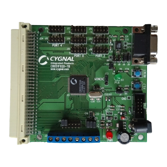
AN172 6. Target Board The C8051F02x Development Kit includes a target board with a C8051F020 device pre-installed for evaluation and preliminary software development. Numerous input/output (I/O) connections are provided to facilitate prototyping using the target board. Refer to Figure 2 for the locations of the various I/O connectors. Power connector (accepts input from 7 to 15 VDC unregulated power adapter) Connects SW2 to P3.7 pin Connects LED D3 to P1.6 pin... - Page 6 AN172 6.1. System Clock Sources The C8051F020 device installed on the target board features a calibrated programmable internal oscillator which is enabled as the system clock source on reset. After reset, the internal oscillator operates at a frequency of 2 MHz (±2%) by default but may be configured by software to operate at other frequencies.
- Page 7 AN172 6.4. Serial Interface (J5) A RS232 transceiver circuit and DB-9 (J5) connector are provided on the target board to facilitate serial connec- tions to UART0 of the C8051F020. The TX, RX, RTS and CTS signals of UART0 may be connected to the DB-9 connector and transceiver by installing shorting blocks on jumpers J6, J8, J9 and J10.
- Page 8 AN172 6.6. PORT I/O Connectors (J12 - J19) In addition to all port I/O signals being routed to the 96-pin expansion connector, each of the eight parallel ports of the C8051F020 has its own 10-pin header connector. Each connector provides a pin for the corresponding port pins 0-7, +3.3 VDC and digital ground.
- Page 9 AN172 6.8. Expansion I/O Connector (J24) The 96-pin expansion I/O connector J24 is used to connect daughter boards to the main target board. J24 provides access to many C8051F020 signal pins. Pins for +3 V, digital ground, analog ground and the unregulated power supply (VUNREG) are also available.
-
Page 10: Serial Adapter
10-pin connector on the Serial Adapter labeled “JTAG”, see Figure 4. (The Serial Adapter supports both Silicon Laboratories JTAG and C2 debug interfaces.). All Serial Adapters may be powered from the target board, but the EC1 and EC2 Serial Adapter units cannot provide power to the target board. Table 7 shows the pin definitions for the Serial Adapter’s JTAG connector. - Page 11 AN172 8. Schematic Rev. 0.4...
-
Page 12: Contact Information
Silicon Laboratories products are not designed, intended, or authorized for use in applications intended to support or sustain life, or for any other application in which the failure of the Silicon Laboratories product could create a situation where per- sonal injury or death may occur.
Need help?
Do you have a question about the C8051F02 Series and is the answer not in the manual?
Questions and answers