Table of Contents
Advertisement
Quick Links
Advertisement
Table of Contents

Related Manuals for Icop VDX-6328RD-NF


Summary of Contents for Icop VDX-6328RD-NF
- Page 1 User Manual VDX-6328RD-NF with DM&P Vortex86DX 800MHz processor Version 1.1...
- Page 2 VDX-6328RD-NF User Manual Copyright The information in this manual is subject to change without notice for continues improvement in the product. All rights are reserved. The manufacturer assumes no reasonability for any inaccuracies that may be contained in this document and makes no commitment to update or to keep current the information contained in this manual.
- Page 3 VDX-6328RD-NF User Manual Revision History Revision Date Remark May 7 2018 First version released Feb 7, 2020 Remove Y cable from cable list...
-
Page 4: Table Of Contents
VDX-6328RD-NF User Manual Table of Contents General Information ........................1 1.1 Packing List ............................1 1.2 Block diagram ........................... 1 1.3 Specifications ............................ 2 1.4 Ordering Information ........................3 Hardware Information ........................4 2.1 Dimension ............................4 2.2 Board Outline and Connector Location ..................5 2.3 Connector and Jumper Summary .................... - Page 5 VDX-6328RD-NF User Manual J19: COM4 ............................12 J25: PC/104 Connector (64pins) ....................13 J26: PC/104 Connector (40pins) ....................14 J27: 4P Power Source (Interconnect to PC/104 – J25) .............. 14 J29: PC/104+ ............................ 15 J30: VGA ............................17 J31: LVDS ............................17 J32 to J38: Display Type Setup (CRT/LCD) ................
- Page 6 VDX-6328RD-NF User Manual TCP/IP Library for DOS Real Mode....................33 BIOS Default Setting ........................... 34 Warranty ..............................35...
-
Page 7: General Information
VDX-6328RD-NF User Manual 1 General Information 1.1 Packing List Product Name Package VDX-6328RD-NF board x1 GPIO cable x1 VDX-6328RD-NF RS232 cable x3 Audio line x2 VDX-6328RD-NF-512 Parallel cable x1 USB cable x1 IDE cable x1 1.2 Block diagram IDM x1... -
Page 8: Specifications
VDX-6328RD-NF User Manual 1.3 Specifications DM&P Vortex86DX 800MHz 256/512MB DDR2 Onboard BIOS AMI BIOS PC/104+ Standard Compliant Display XGI Volari Z9s Chipset with VGA, TFT-LCD, and 18-bit LVDS Flat Panel Interface Support and onboard 32MB VGA memory VGA: Maximum resolution up to 1280 x 1024 @ 60Hz... -
Page 9: Ordering Information
VDX-6328RD-NF User Manual Operating -20 - +70°C Temperature -40 - +85°C (Optional) Dimension 102 x 146mm Weight 150g O/S Support Windows Embedded 2009 Free BSD Windows Embedded CE6.0 Windows Embedded CE 5.0 POS Ready (WePOS) Linux VxWorks 1.4 Ordering Information PART NO. -
Page 10: Hardware Information
VDX-6328RD-NF User Manual 2 Hardware Information 2.1 Dimension... -
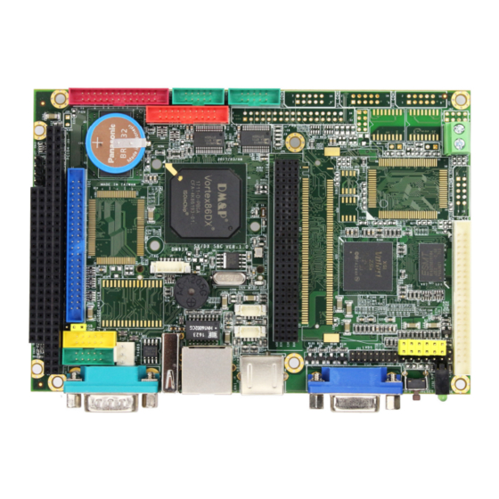
Page 11: Board Outline And Connector Location
VDX-6328RD-NF User Manual 2.2 Board Outline and Connector Location Note: 1. VI/O Default setting of PCI-104 connector is DC +5V. 2. COM2 can be configured as RS232/422/485 by BIOS setting. 3. VDX-6328RD-NF is optional. -
Page 12: Connector And Jumper Summary
VDX-6328RD-NF User Manual 2.3 Connector and Jumper Summary Nbr. Name Type of Connections Pin of Nbr. Box Header, 2.0mm, 22x2 Jumper Switch for Pin Header, 2.54mm, 2x1 CF Mater/Slave USB2 Type A USB Connector USB1 Box Header, 2.0mm, 5x2 RJ45 connector Reset Pin Header, 2.54mm, 1x2... - Page 13 VDX-6328RD-NF User Manual IDE Active (Green) MTBF MTBF LED (Orange) LED SMD Buzzer Reset Switch...
-
Page 14: Pin Assignments & Jumper Settings
VDX-6328RD-NF User Manual 2.4 Pin Assignments & Jumper Settings J1: IDE Pin# Signal Name Pin # Signal Name IDERST IDED7 IDED8 IDED6 IDED9 IDED5 IDED10 IDED4 IDED11 IDED3 IDED12 IDED2 IDED13 IDED1 IDED14 IDED0 IDED15 IDEREQ IDEIOW IDEIOR ICHRDY IDEACK... -
Page 15: J4: Usb1
VDX-6328RD-NF User Manual J4: USB1 Pin# Signal Name Pin # Signal Name LUSBD0- LUSBD1- LUSBD0+ LUSBD1+ GGND GGND J6: LAN Pin# Signal Name Pin # Signal Name J7: Reset Pin# Signal Name Pin # Signal Name Reset J9: PS/2 Connector (for Keyboard/Mouse) -
Page 16: J10: Com1 (Optional: Ttl/Gpio-P4/Pwm X8)
VDX-6328RD-NF User Manual J10: COM1 (Optional: TTL/GPIO-P4/PWM x8) Pin# Signal Name Pin # Signal Name DCD1 RXD1 TXD1 DTR1 DSR1 RTS1 CTS1 J11: GPIO (Port0/1 or PWM x8) Pin# Signal Name Pin # Signal Name GP00 GP10 GP01 GP11 GP02... -
Page 17: J15: Rs485 (Auto Direction)
VDX-6328RD-NF User Manual J15: RS485 (Auto direction) Pin# Signal Name RS485+ RS485- J16: Power Connector Pin# Signal Name J17: COM3 Pin# Signal Name Pin # Signal Name DCD3 RXD3 TXD3 DTR3 DSR3 RTS3 CTS3... -
Page 18: J18: Parallel
VDX-6328RD-NF User Manual J18: Parallel Pin# Signal Name Pin # Signal Name STB- AFD- ERR- INIT- SLIN- ACK- BUSY SLCT J19: COM4 Pin# Signal Name Pin # Signal Name DCD4 RXD4 TXD4 DTR4 DSR4 RTS4 CTS4... -
Page 19: J25: Pc/104 Connector (64Pins)
VDX-6328RD-NF User Manual J25: PC/104 Connector (64pins) Pin# Signal Name Pin # Signal Name IOCHCHK* RESETDRV IRQ9 DRQ2 -12V +12V IOCHRDY SMEMW* SA19 SMEMR* SA18 IOW* SA17 IOR* SA16 DACK3* SA15 DRQ3* SA14 DACK1* SA13 DRQ1* SA12 REFRESH* SA11 SYSCLK... -
Page 20: J26: Pc/104 Connector (40Pins)
VDX-6328RD-NF User Manual J26: PC/104 Connector (40pins) Pin# Signal Name Pin # Signal Name MEMSC16* SBHE* IOCS16* SA23 IRQ10 SA22 IRQ11 SA21 IRQ12 SA20 IRQ15 SA19 IRQ14 SA18 DACK0* SA17 DRQ0 MEMR* DACK5* MEMW* DRQ5 DACK6* DRQ6 SD10 DACK7* SD11... -
Page 21: J29: Pc/104
VDX-6328RD-NF User Manual J29: PC/104+ VI/O Default Setting: +5V; If +3.3v is required, please see the page 16. Pin# AD00 VIO (+5V) AD02 AD01 AD05 AD04 AD03 C/BE0# AD07 AD06 AD09 AD08 AD11 VIO (+5V) AD10 AD14 AD13 AD12 +3,3V C.BE1#... - Page 22 VDX-6328RD-NF User Manual Pleas remove 0 ohm (1206 type) of R260 and add 0 ohm (1206 type) on R261.
-
Page 23: J30: Vga
VDX-6328RD-NF User Manual J30: VGA Pin# Signal Name Pin # Signal Name ROUT GOUT BOUT DDCDAT HSYNC VSYNC DDCCLK J31: LVDS Pin# Signal Name Pin # Signal Name VCC3 VCC3 RxIN0+ RxIN0- RxIN1- RxIN1+ RxIN2+ RxIN2- CKIN- CKIN+... -
Page 24: J32 To J38: Display Type Setup (Crt/Lcd)
VDX-6328RD-NF User Manual J32 to J38: Display Type Setup (CRT/LCD) Pin# Signal Name Pin # Signal Name GPIOA GPIOB GPIOC GPIOD GPIOE GPIOF For more details, please refer to Appendix for display type setup. -
Page 25: J33: Lcd (Dvo) Connector
VDX-6328RD-NF User Manual J33: LCD (DVO) Connector Pin# Signal Name Pin # Signal Name +3.3V +3.3V LCLK LHSYNC LVSYNV LBACKL LVVDEN For TFT Flat Panel Data Output, please refer to Appendix. J40: Lint-out J41: MIC-in Pin# Signal Name Pin# Signal Name... -
Page 26: System Mapping
VDX-6328RD-NF User Manual 2.5 System Mapping Memory Mapping Address Description Usage 0000:0000 – 9000:FFFF System RAM A000:0000 – A000:FFFF EGA/VGA Video Memory B000:0000 – B000:7FFF MDA RAM, Hercules graphics display RAM B000:8000 – B000:FFFF CGA display RAM C000:0000 – C000:7FFF EGA/VGA BIOS RAM C000:8000 –... - Page 27 VDX-6328RD-NF User Manual 0065h Watchdog 0 Reload Counter 0066h 8051 Download 8-bit Data Port 0067h Watchdog 1 Reload Counter 0068h – 006Dh Watchdog 1 Control Register 006Eh – 006Fh Empty 0070h – 0071h CMOS RAM port 0072h – 0075h MTBF counter...
- Page 28 VDX-6328RD-NF User Manual 0CF8h – 0CFFh PCI Configuration Port D400h – D4FFh Onboard LAN FC00h – FC05h SPI Flash BIOS Control Register FC08h – FC0Dh External SPI Bus Control Register (Output pin configurable GPIO3 [0 -3])\ IRQ Mapping IRQ# Description...
-
Page 29: Watchdog Timer
VDX-6328RD-NF User Manual Watchdog Timer Two watchdog timers are equipped in Vortex86DX SoC. One is compatible with M6117D watchdog timer and the other one is new. The M6117D compatible watchdog timer is called WDT0 and the new one is called WDT1. -
Page 30: Pwm
VDX-6328RD-NF User Manual Pulse-width modulation (PWM) of a signal or power source involves the modulation of its duty cycle, to either convey information over a communications channel or control the amount of power sent to a load. The popular applications of pulse width modulation are in speed control of electric motors, volume control of Class D audio amplifiers or brightness control of light sources and many other power electronics applications. -
Page 31: Ide To Micro Sd
VDX-6328RD-NF User Manual 2.10 IDE to Micro SD Vortex86DX SoC also built-in simulation circuit to adapt SD to IDE in order to allow your system to recognize microSD card as C: or D: Driver SD-1917: 44 pins IDE to SD Adapter is an ideal solution for industrial PC or embedded system and 44 pins IDE to SD Adapter can be easily installed on all Vortex86DX-63xx CPU boards. -
Page 32: Driver Installation
VDX-6328RD-NF User Manual 3 Driver Installation The Vortex86DX processor also use external Display chip ““Volari™ Z9s” which is an ultra low powered graphics chipset with total power consumption at around 1-1.5 W. It is capable in providing VGA display output upto 1600x1200. With DVO interface, developers could easily connect flat Panel to support TFT and LVDS output. -
Page 33: Software Resources
VDX-6328RD-NF User Manual 4 Software Resources 4.1 Technical Resource Website In the following website, you will find our latest user manuals, including OS ssupport resources systems such as evaluation images for 32-bit Window operating systems. -
Page 34: Technical Support Directly From
VDX-6328RD-NF User Manual Technical Support Directly from To offer you more accurate and specific solutions for the technical situations you have, please prepare the information below before contacting: —Product name and serial number —Description of the H/W environment ( i.e.: working temperature, I/O... -
Page 35: Appendix
VDX-6328RD-NF User Manual Appendix TFT Flash Panel Data Output... -
Page 36: Tft Flash Panel Support List
VDX-6328RD-NF User Manual TFT Flash Panel Support List Size Brand Resolution Model No. 5.7” Data image 320x240 FG050701DSSWBG01 5.7” Optrex 320x240 55264GD057J-FW-ABN 5.7” TOSHIBA 320x240 LTA057A343F 5.7” Sharp 320x240 (QVGA / VGA) LQ057Q3DC02 5.7” Kyocera 320x240 (QVGA / VGA) TCG057QV1AC-G10 5.7”... - Page 37 VDX-6328RD-NF User Manual Size Brand Resolution Model No. 8” 800x600 (TFT 24bits) A080SN01 V0 8.4” Sharp 800x600 LQ084S3DG01 10.4” 640x480 PD104VT1/VT2 10.4” 640x480 NL6448AC33-18 10.4” 640x480 NL6448AC33-29 10.4” 640x480 NL6448BC33-59 10.4” Sharp 640x480 LQ104V1DG51/DG61 10.4” Sharp 640x480 LQ10d368 11” Sharp...
-
Page 38: Flat Panel Hardware Setting
VDX-6328RD-NF User Manual Flat Panel Hardware Setting The VDX-6328RD offers the Hardware setting for the various TFT LCD Flat Panels support and please make sure the jumper setting (J32~J38) before you connect the LCD. Display Type Setup Connector C: Close... -
Page 39: Flat Panel Wiring And Lighting
Application systems: Mity-Mite Serial Server, Web Camera Tiny Server and RSIP Serial Server. DSock is free for All ICOP products using M6117D/Vortex86/Vortex86SX/Vortex86DX CPU and ICOP also provide the business version of DSock for those customers who are using other x86 CPUs. - Page 40 VDX-6328RD-NF User Manual BIOS Default Setting If the system cannot be booted after BIOS changes are made, Please follow below procedures in order to restore the CMOS as default setting. Press “End” Key, when the power on Press <Del> to enter the AMI BIOS setup ...
- Page 41 VDX-6328RD-NF User Manual Warranty This product is warranted to be in good working order for a period of one year (12 months) from the date of purchase. Should this product fail to be in good working order at any time during this period, we will, at our option, replace or repair it without additional charge except as set forth in the following terms.
Need help?
Do you have a question about the VDX-6328RD-NF and is the answer not in the manual?
Questions and answers