
Related Manuals for DTK PRM-89I


Summary of Contents for DTK PRM-89I
- Page 1 PRM-89I High Performance Pentium II PCI Mainboard User’s Guide Edition 1.00 © 1998 DTK Computer, Inc. P/N: 155100-8747...
- Page 2 WARNING For the system to operate normally, please make sure J5 of the mainboard is set as below. Refer to Fig. 2 in this manual for the location J5. If J5 is shorted to 2-3, no CMOS data can be retained. CAUTION The motherboard is an electrostatic sensitive device.
-
Page 3: Table Of Contents
CONTENTS CHAPTER 1 INTRODUCTION CHAPTER 2 JUMPER SETTINGS JUMPERS PRESENTATION GRAPHICAL DESCRIPTION OF JUMPER SETTINGS CPU SPEED J5 - CLEAR CMOS DATA J2 - VOLTAGE SELECTION FOR SYSTEM ROM MEMORY CONFIGUARTION CHAPTER 3 CONNECTOR CONFIGURATION JP1 - IrDA CONNECTOR JP8 - ATX POWER SUPPLY CONNECTOR JP10 - FLOPPY DRIVE CONTROLLER JP11, JP12 –... - Page 4 CHAPTER 5 FLASH AND DMI UTILITY AWARD FLASH UTILITY DESKTOP MANAGEMENT INTERFACE (DMI) OVERVIEW APPENDIX A QUICK GUIDE...
-
Page 5: Introduction
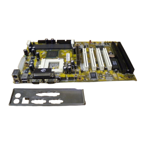
CHAPTER 1 INTRODUCTION Preface The motherboard is a 4 layers, ATX form factor high performance PCI/AGP mainboard. It includes Intel i82440LX system chipset, Winbond W83977EF Super I/O controller. Features Processor • Intel PPGA P370 series. • The mainboard can run with following speeds: 300A, 333, 366 and 400 MHz •... - Page 6 Chapter 1 System BIOS • Award BIOS (256KB Flash EPROM). Slots • One AGP slot • Four PCI slots • Two ISA slots Form Factor • ATX Form Factor Size (305mm x 185mm) 4 Layers Fig. 1 Key Components of the Mainboard...
-
Page 7: Jumper Settings
CHAPTER 2 JUMPER SETTINGS JUMPERS PRESENTATION Pins 1 and 2 are shorted with a jumper cap. Pins 2 and 3 are shorted with a jumper cap. The jumper is shorted when the jumper cap is placed over the two pins of the jumper. The jumper is open when the jumper cap is removed from jumper. -
Page 8: Graphical Description Of Jumper Settings
Chapter 2 GRAPHICAL DESCRIPTION OF JUMPER SETTINGS Fig. 2 Jumper Location of the mainboard... -
Page 9: Cpu Speed
Jumper Settings CPU SPEED The table below summaries the CPU frequency and settings of each jumper of the motherboard. CPU Type Freq. Bus Freq. 300MHz 333MHz PPGA P370 66MHz Mendocino 366MHz 400MHz Table 1 J5 - CLEAR CMOS DATA J5 is used to clear the content of the CMOS Data in the RTC (build in PIIX4 chip). Table 2: Clear CMOS Data... -
Page 10: J2 - Voltage Selection For System Rom
Chapter 2 J2 - VOLTAGE SELECTION FOR SYSTEM ROM J2 is used to select the operation voltage of the system ROM. Table 3: Voltage Selection for System ROM MEMORY CONFIGUARTION The mainboard lets user upgrade system memory via DIMM sockets on the mainboard. -
Page 11: Connector Configuration
CHAPTER 3 CONNECTOR CONFIGURATION Once the mainboard has been fastened into system case, the next step is to connect the internal cables. The internal cables are wire leads with plastic female connectors that attach to the connectors. The mainboard connectors have varying numbers of pins and are the points of contact between the mainboard and other parts of the computer. -
Page 12: Jp1 - Irda Connector
Chapter 3 JP1 - IrDA CONNECTOR JP1 is an IrDA connector that use UART2 as interface of IrDA Infrared and ASKIR. Fig. 4 IrDA Connector JP8 - ATX POWER SUPPLY CONNECTOR Fig. 5 ATX Power Supply Connector JP10 - FLOPPY DRIVE CONTROLLER This connector supports the floppy drive ribbon cable. -
Page 13: Jp11, Jp12 - Secondary/Primary Ide Connectors
Connector Configuration JP11, JP12 – SECONDARY/PRIMARY IDE CONNECTORS These connectors support the provided IDE hard disk ribbon cable. After connecting the single end to the board, connect the two plugs on the other end to your hard disk or other device. JP13 - HDD LED JP13 is usually connected to a HDD LED on front of the system case. -
Page 14: Jp17 - Speaker
Chapter 3 JP17 - SPEAKER JP17 is a four-pin connector, which is used to connect the system speaker. Fig. 8 Speaker 3.10 FAN2 – CPU FAN CONNECTOR FAN2 is a three-pin connector, which is used to connect with the CPU Fan Power cable. -
Page 15: Ps/2 Keyboard Connector
Connector Configuration Fig. 10 I/O Connector 3.13 PS/2 KEYBOARD CONNECTOR This connector is a six-pin female mini DIN connector using a PS/2 plug. If a standard AT size keyboard plugs, you may use the DIN to mini DIN adaptor. 3.14 PS/2 MOUSE CONNECTOR This connector is a six-pin female mini DIN connector using a PS/2 plug. - Page 16 Chapter 3...
-
Page 17: Award Bios Setup Guide
CHAPTER 4 AWARD BIOS SETUP GUIDE This following manual is specially provided for the BIOS supported system. After the configuration of the mainboard, and have assembled the components, user can turn on the completed system. At this point, run the software setup to ensure that the system information is correct. - Page 18 Chapter 4 Press the <DEL> key to enter the AWARD BIOS setup program and the following screen appears: ROM PCI/ISA BIOS (2A69JD1J) CMOS SETUP UTILITY AWARD SOFTWARE, INC. STANDARD CMOS SETUP INTEGRATED PERIPHERALS BIOS FEATURES SETUP SUPERVISOR PASSWORD CHIPSET FEATURES SETUP USER PASSWORD POWER MANAGEMENT SETUP IDE HDD AUTO DETECTION...
-
Page 19: Standard Cmos Setup
Award BIOS Setup Guide STANDARD CMOS SETUP ROM PCI/ISA BIOS (2A69JD1J) STANDARD CMOS SETUP AWARD SOFTWARE, INC. Date (mm:dd:yy) : Wed, Dec 11 1998 Time (hh:mm:ss) : 20 : 27 : 55 HARD DISKS TYPE SIZE CYLS HEAD PRECOMP LANDZ SECTOR MODE Primary Master : Auto AUTO... -
Page 20: Bios Features Setup
Chapter 4 BIOS FEATURES SETUP ROM PCI/ISA BIOS (2A69JD1J) BIOS FEATURES SETUP AWARD SOFTWARE, INC. Virus Warning : Enabled Video BIOS Shadow : Disabled CPU Internal Cache : Enabled C8000-CBFFF Shadow : Disabled External Cache : Enabled CC000-CFFFF Shadow : Disabled Quick Power On Self Test : Enabled D0000-D3FFF Shadow... - Page 21 Award BIOS Setup Guide Boot Sequence: With the default setting the BIOS first attempts to boot from drive A: and then, if unsuccessful, from hard disk C:. User can select other boot up sequence. Available sequences are “A,C,SCSI”, “C,A,SCSI”, “C,CDROM,A”, “CDROM,C,A”, “D,A,SCSI”, “E,A,SCSI”, “F,A,SCSI”, “SCSI,A,C”, “SCSI,C,A”, “C only”, “LS120,C”.
-
Page 22: Chipset Features Setup
Chapter 4 Report No FDD For WIN 95: Choose Yes or No. Yes will show a removable disk in Windows 95 when the floppy drive is set as None. Video BIOS Shadow: ROM Shadow copies Video BIOS code from slower ROM to faster RAM. Video BIOS can then execute from RAM. - Page 23 Award BIOS Setup Guide A short description of the screen items follows: Auto Configuration: When Auto Configuration is Enabled, BIOS will sets the CPU Clock according to CPU speed. Otherwise, set it manually. DRAM Speed Selection: Choose 60ns or 70ns according to the DRAM SIMM Module on the motherboard.
-
Page 24: Power Management Setup Menu
Chapter 4 Auto Detect DIMM/PCI Clk: Enabled is auto-detect DIMM or PCI card. If exist will delivery clock or won’t delivery clock. Disabled will always delivery clock. Spread spectrum: Enabled allows clock gen. Generate spectrum clock to inhibit EMI. Select Disabled won’t pass EMI. - Page 25 Award BIOS Setup Guide Power Management: Available selections are “Disabled”, “User Define”, “Max “Disabled” will disable all the power saving functions. “User Define” makes the time period waiting for Suspend Mode to be programmed. “Max Saving” will set the time period waiting for Suspend Mode to be 20 seconds. “Min Saving”...
-
Page 26: Pci Configuration
Chapter 4 Reload Global Timer Event: When Enabled, an event occurring on each device listed below restarts the global time for Standby Mode. IRQ[3-7,9-15], NMI Primary IDE 0 Primary IDE 1 Secondary IDE 0 Secondary IDE 1 Floppy Disk Serial Port Parallel Port PCI CONFIGURATION The PCI Configuration Setup option is used to configure the PCI add-on Cards on PCI... - Page 27 Award BIOS Setup Guide A short description of the screen items follows: PNP OS Installed: Set this option to Yes if the operating system installed in the computer is Plug and Play-aware (e.g. Windows 95). Resources Controlled By: The Award Plug and Play BIOS can automatically configure all the boot and Plug and Play compatible device.
-
Page 28: Integrated Peripherals Setup Menu
Chapter 4 INTEGRATED PERIPHERALS SETUP MENU The Integrated Peripherals setup option is need to change the values of the I/O chipset registers for I/O functions. ROM PCI/ISA BIOS (2A69JD1J) INTEGRATED PERIPHERALS AWARD SOFTWARE, INC. IDE HDD Block Mode : Enabled Onboard Serial Port2 : 2F8/IRQ3 IDE Primary Master PIO... - Page 29 Award BIOS Setup Guide IDE Primary Master UDMA/IDE Primary Slave UDMA/IDE Secondary Master UDMA/IDE Secondary Slave UDMA: Available selections are “Auto” or “Disabled”. To choose “Auto”, the system BIOS will scan the IDE device and decide Ultra DMA supported or not.
-
Page 30: Load Setup Defaults Menu
Chapter 4 POWER After PWR-Fail: If select OFF when AC is stop suddenly later AC appear again power will all off. If select ON when AC is stop suddenly later AC appear again that power will always on. If select Former-Sts when AC is stop suddenly later AC appear again. It will be according that prevision state to ON or OFF. -
Page 31: User Password
Award BIOS Setup Guide 4.10 USER PASSWORD With the user password, only booting up the system is accepted, but changing the BIOS setup is not allowed. 4.11 IDE HDD AUTO DETECTION When users can not find the Hard Disk information, it is very helpful to use this option. Choose this item and press <Enter>. -
Page 32: Exit Without Saving Menu
Chapter 4 4.14 EXIT WITHOUT SAVING MENU When you select this function, the following message will appear at the centre of the screen to assist you to Abandon all Data and Exit Setup. Quit Without Saving (Y/N)? - Page 33 CHAPTER 5 FLASH AND DMI UTILITY AWARD FLASH UTILITY This section will provide instructions to guide you through updating your old BIOS. The file name we use to program here is test.bin, and the file name to save old BIOS is 2A69JD1J.OLD.
- Page 34 Chapter 5 If you do not wish to save the old BIOS: Please type “N”, and then press the ENTER key. Then you will be request to answer: “Are You Sure to Program?” Answer “N” if you do not want to program, and then it will exit. To save the old BIOS: Please respond “Y”, and then press the ENTER key.
- Page 35 Flash and DMI Utility DESKTOP MANAGEMENT INTERFACE (DMI) OVERVIEW This motherboard can support DMI within the BIOS level. DMI is able to auto- detect and record information pertinent to a computer’s system such as the CPU type, CPU speed, and internal/external frequencies, and memory size. The onboard BIOS will detect as many system information as possible and store those collected information in a 4KB block in the motherboard’s flash EPROM and allow the DMI to retrieve data from this database.
- Page 36 Chapter 5 Use the ←→ (left-right) cursors to move the top menu items and the ↑↓ (up-down) cursor to move between the left hand menu items. The bottom of the screen will show the available keys for each screen. Press enter at the menu item to enter the right hand screen for editing. “Edit component”...
- Page 37 Flash and DMI Utility Load DMI File You can load the disk file to memory by entering a drive and path and file name here.
- Page 38 Chapter 5 Save DMI File You can save the DMI (normally only saved to flash ROM) to a file by entering the drive and path here. If you want to cancel save, you may press ESC and a message “Bad File Name” appears here to show it was not saved.
- Page 39 APPENDIX A QUICK GUIDE The table below summaries the functions and settings of each jumper of the motherboard. Function Jumper Settings Normal 1-2 short Clear CMOS Data Clear 2-3 short 5V Flash EPROM 1-2 short System ROM Selection 12V Flash EPROM 2-3 short...
Need help?
Do you have a question about the PRM-89I and is the answer not in the manual?
Questions and answers