
Related Manuals for Jäger ADwin-Pro


Summary of Contents for Jäger ADwin-Pro
- Page 1 ADwin-Pro, -Pro II System and hardware description ADwin-Pro Hardware, manual version 2.9, June 2006...
- Page 2 For any questions, please don’t hesitate to contact us: Hotline: +49 6251 96320 Fax: +49 6251 5 68 19 Jäger Computergesteuerte E-Mail: info@ADwin.de Messtechnik GmbH Rheinstraße 2-4 Internet www.ADwin.de D-64653 Lorsch Germany ADwin-Pro Hardware, manual version 2.9, June 2006...
-
Page 3: Table Of Contents
4 Enclosures for the ADwin-Pro System ........ -
Page 4: Typographical Conventions
Courier New and are printed in color (see also the editor of the ADbasic development environment). Bits in data (here: 16 bit) are referred to as follows: Bit No. … Bit value … Synonym ADwin-Pro Hardware, manual version 2.9, June 2006... -
Page 5: The Adwin-Pro System
The revision identifier is followed by a minor counting number, which is mainly used for internal purposes of Jaeger Computergesteuerte Messtechnik GmbH. All modules for ADwin-Pro II have the revision identifier Rev. E1 or higher. This is true for both advancements out of Pro I modules and for newly developped modules. -
Page 6: How To Install An Adwin-Pro System
ADwin How to Install an ADwin-Pro System 2 How to Install an ADwin-Pro System Please keep strictly to the following order: 1. Start with the manual "ADwin installation": • Installation of software and interface drivers from the ADwin-CDROM. • Initialization of data connection from PC to ADwin system as well as operational test. -
Page 7: Operating Environment
Close the device for operation, use cover plates to cover gaps between built-in modules. ADwin-Pro is designed for operation in dry rooms with an ambient temperature Ambient atmosphere of +5°C … +50°C and a relative humidity of 0 … 80% (no condensation). The device may be operated in a control cabinet or mobile (e.g. -
Page 8: Enclosures For The Adwin-Pro System
10V…18V ADwin-Pro-mini-3 20V…36V With ADwin-Pro II systems, the number of slots is given for Pro II modules. If Pro I modules be used – in combination with Pro II modules or not – less mod- ules fit into the enclosure For the slot area (including power supply slot) the following dimensions apply: 1 HP = 1/5 inch = 5.08mm... -
Page 9: Adwin-Pro
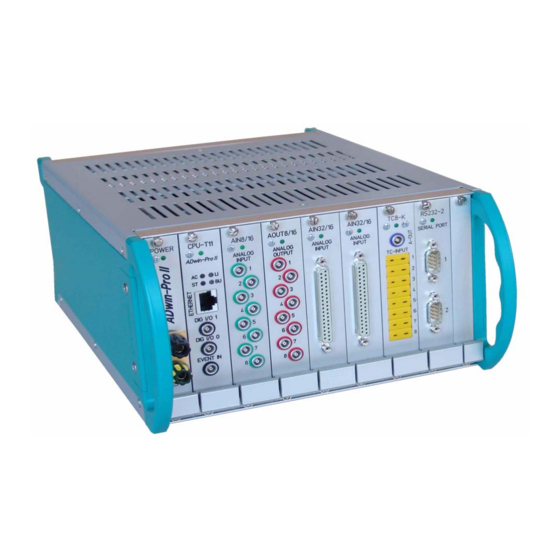
ADwin ADwin-Pro 4.1 ADwin-Pro The standard enclosure for the ADwin-Pro systems. The backplane of the Pro with 16 slots enclosure connects the processor module with the ADwin-Pro modules. The system fuse is located in a slot in the power supply unit above the socket for the power supply cable (rear of the enclosure). - Page 10 Modules for Pro I-Bus Modules for Pro I-Bus EVENT IN 10 11 12 13 Fig. 3 – Enclosure ADwin-Pro II (up from Rev. E1) Please note that modules for Pro I bus (grey in fig. 3) and for Pro II bus have different plug-in positions.
-
Page 11: Adwin-Pro-Dc
ADwin ADwin-Pro-DC 4.2 ADwin-Pro-DC The ADwin-Pro-DC enclosure is similar to the standard enclosure ADwin-Pro, Pro-DC but is equipped with a DC power supply. with 16 slots If a current-limited power supply unit is used, it should be able to supply a mul- tiple of the idle current during power-up to maintain proper performance of the system. -
Page 12: Adwin-Pro-Bm
The revisions are similar to those of the ADwin-Pro enclosure. POWER 230V 11 12 13 115 / 230 VAC Fig. 6 – Enclosure of ADwin-Pro I-BM (rear panel) POWER CPU-T11 ADwin-Pro 230V 11 12 13 DIG I/O 1 DIG I/O 0... -
Page 13: Adwin-Pro-Light
DIG I/O 0 EVENT IN Enclosure ADwin-Pro I-light Enclosure ADwin-Pro II-light The ADwin-Pro-light enclosure. The backplane of the enclosure connects the processor module with the ADwin-Pro modules. Number of Slots Main dimensions (l x w x h) 336mm × 234mm × 146mm Slot area (w x h) 42 HP ×... -
Page 14: Adwin-Pro-Mini
ADwin ADwin-Pro-mini 4.5 ADwin-Pro-mini The ADwin-Pro-mini enclosure is available in 3 versions, each of which works with a different power supply voltage. In any case an external power supply unit is required. The enclosure type ADwin-Pro-mini for Pro II is being developped. -
Page 15: Adwin-Pro Modules
ADwin ADwin-Pro Modules 5 ADwin-Pro Modules An ADwin-Pro module needs one slot (5 HP) in an ADwin-Pro system, some modules need 2 slots. All technical data of the module refer to a device which is powered-up. For pluggin-in a module into the enclosure please note the description on page 4, especially with ADwin-Pro II enclosures. - Page 16 Settings of DIP switches Module no. … … Fig. 13 – Address settings of the ADwin-Pro modules with DIP switches Please note: – A RSxxx module with 4 serial interfaces uses 2 addresses (group EXT): the set address and the following address.
-
Page 17: Processor Modules
ADwin Processor modules 5.2 Processor modules For each ADwin-Pro system one processor module is required. This processor module is the center of a Pro system and performs the following tasks: – Communication with PC or laptop. The data connection is established via USB or Ethernet; former version used a serial link connection. - Page 18 LINK OUT (-) /ANALYSE /ERROE LINK IN (+) LINK IN (-) Fig. 18 – Pro-CPU-T9: Pin assignment CPU-T9 19DSPIF01 ADwin-Pro LINK ADSP-21062 FPGA EVENT IN DC-DC-converter Fig. 19 – Pro-CPU-T9: Board and front panel ADwin-Pro Hardware, manual version 2.9, June 2006...
- Page 19 Fig. 21 – Pro-CPU-T9-ENET / -USB: Specifikation CPU-T9 19ADSP03 ADwin-Pro LM2937ES LM3940IS -2.5 -3.3 STAT BUSY ADSP-21062 ETHERNET FPGA EVENT IN Xilinx SPARTAN XC2S50 24MHz 40MHz 19ARM12 Fig. 22 – Pro-CPU-T9-ENET: Board and front panel ADwin-Pro Hardware, manual version 2.9, June 2006...
- Page 20 ADwin Processor modules CPU-T9 ADwin-Pro LM2937ES LM3940IS -2.5 -3.3 ADSP-21062 USB- Cypress AN2135 FPGA EVENT IN Xilinx SPARTAN XC2S50 AT17LV010 24MHz 40MHz Fig. 23 – Pro-CPU-T9-USB: Board and front panel ADwin-Pro Hardware, manual version 2.9, June 2006...
- Page 21 AN2135 21160 FPGA DIG IN 0 40MHz Xilinx EVENT IN SPARTAN XC2S50 AT17LV010 24MHz Fig. 26 – Pro-CPU-T10-ENET: Board and front panel The input Digin 0 is for use with TTL signals only. ADwin-Pro Hardware, manual version 2.9, June 2006...
- Page 22 All referring values and calculations must be adapted to the new time unit. The greatest possible Processdelay corresponds to 7.1 s; a greater cycle time can be achieved using an auxiliary variable. ADwin-Pro Hardware, manual version 2.9, June 2006...
- Page 23 1. The processor architecture differs from T9 and T10 in this point: T9 and T10 processed instruc- tions of both groups sequentially. Thus, halting the processor with a SLEEP instruction did make the waiting time for subsequent I/O instructions, too. ADwin-Pro Hardware, manual version 2.9, June 2006...
- Page 24 If you use the boot loader, an application, which you have written with a pro- gram for visualization of measurement data, must not reboot the ADwin sys- tem. ADwin-Pro Hardware, manual version 2.9, June 2006...
- Page 25 You can monitor your processor module with a watchdog. The watchdog gen- erates a reset, when a signal, generated by a program code, does unexpect- edly not arrive (see also "ADwin-Pro System Specifications - Programming in ADbasic"). This reset sets the digital and analog outputs to those values, which correspond to the configuration after power-up, normally digital 0 or 0 Volt.
- Page 26 ADwin Processor modules ADwin-Pro Hardware, manual version 2.9, June 2006...
-
Page 27: Pro Ii: Analog Input Modules
ADwin Pro II: Analog Input Modules 5.3 Pro II: Analog Input Modules This section describes analog input modules for ADwin-Pro II. Analog input modules for ADwin-Pro I be found on page 38 Module name 8/18 32/18 F-8/14 F-8/18 Revision Number ADC Resolution [Bit] Conv. - Page 28 Accuracy ±3 LSB typical max. ±1 LSB Input resistance 330kΩ, ±2% Input over-voltage ±35V Offset error adjustable Offset drift ±30ppm/ºC Connector 8 LEMO sockets, 2-pole Fig. 31 – Pro II-AIn-8/18-L2 Rev. E: Specification ADwin-Pro Hardware, manual version 2.9, June 2006...
- Page 29 Pro II: Analog Input Modules Pro II-AIn-8/18-L2 Rev. E AIN8/18 ANALOG INPUT +AIN −AIN Zoom 2-pole LEMO socket; series 00 Multi-Con- tact, type EGG Fig. 32 – Pro II-AIn-8/18-L2 Rev. E: Front panel ADwin-Pro Hardware, manual version 2.9, June 2006...
- Page 30 1, 2, 4, 8 software selectable Accuracy ±3 LSB typical max. ±1 LSB Input resistance: 330kΩ, ±2% Input over-voltage: ±35V Offset error: adjustable Offset drift: ±30ppm/ºC Connector: 37-pin DSub socket Fig. 34 – Pro II-AIn-32/18-D Rev. E: Specification ADwin-Pro Hardware, manual version 2.9, June 2006...
- Page 31 DC/DC CONVERTER IN 5V OUT ±15V / ±65mA 40MHz XILINX ® XC2S200 19AD1002 DIP switch to the right: Isolation from ground ON Fig. 37 – Pro II-AIn-32/18-D Rev. E: Board and front panel ADwin-Pro Hardware, manual version 2.9, June 2006...
- Page 32 As an option one channel of the burst sequence may be used as time channel, which holds the counter value of the internal module timer for each event sig- nal. ADwin-Pro Hardware, manual version 2.9, June 2006...
- Page 33 3 differential; RS422/485 compatible (5 V differential, 120 Ω bus terminating resistor) Connector 8 LEMO sockets. 2-pole optional: 37-pin DSub socket optional: 8 BNC sockets. Fig. 39 – Pro II-AIn-F-8/14 Rev. E: Specification ADwin-Pro Hardware, manual version 2.9, June 2006...
- Page 34 + AIN − AIN Zoom 2-pole LEMO s o c k e t ; s e r i e s 0 0 Multi-Contact, type Fig. 41 – Pro II-AIn-F-8/14 Rev. E: Front panels ADwin-Pro Hardware, manual version 2.9, June 2006...
- Page 35 Input resistance 330kΩ, ±2% Input over-voltage ±35V Offset error adjustable Offset drift ±30ppm/ºC of full scale range Steckerverbindung 8 LEMO sockets, 2-pole optional: 37-pin DSub socket Fig. 43 – Pro II-AIn-F-8/18 Rev. E: Specification ADwin-Pro Hardware, manual version 2.9, June 2006...
- Page 36 + AIN − AIN Zoom 2-pole LEMO s o c k e t ; s e r i e s 0 0 Multi-Contact, type Fig. 45 – Pro II-AIn-F-8/18 Rev. E: Front panels ADwin-Pro Hardware, manual version 2.9, June 2006...
-
Page 37: Pro Ii: Analog Output Modules
ADwin Pro II: Analog Output Modules 5.4 Pro II: Analog Output Modules This section describes analog input modules for ADwin-Pro II. Analog output modules for ADwin-Pro I be found from page AOut AOut Module name 4/16 8/16 Revision Number DAC Resolution [bit] max. - Page 38 Accuracy ±2 LSB typical ±1 LSB typical Offset error adjustable Gain error adjustable Offset drift ±10 µV/ºC Connector 4 LEMO sockets optional: 37-pin D-SUB socket Fig. 47 – Pro II-AOut-4/16 Rev. E: Specification ADwin-Pro Hardware, manual version 2.9, June 2006...
- Page 39 ANALOG OUT 1 ANALOG ANALOG ANALOG OUT 2 OUTPUT OUTPUT ANALOG OUT 3 ANALOG OUT 4 AGND RESERVED RESERVED EVENT DGND Fig. 48 – Pro II-AOut-4/16 Rev. E: Pin assignment DSub and front cover ADwin-Pro Hardware, manual version 2.9, June 2006...
- Page 40 Accuracy ±2 LSB typical ±1 LSB typical Offset error adjustable Gain error adjustable Offset drift ±10 µV/ºC Connector 8 LEMO sockets optional: 37-pin D-SUB socket Fig. 50 – Pro II-AOut-8/16 Rev. E: Specification ADwin-Pro Hardware, manual version 2.9, June 2006...
- Page 41 ANALOG OUT 4 AGND ANALOG OUT 5 ANALOG OUT 6 ANALOG OUT 7 ANALOG OUT 8 RESERVED RESERVED EVENT DGND Fig. 51 – Pro II-AOut-8/16 Rev. E: Pin assignment DSub and front cover ADwin-Pro Hardware, manual version 2.9, June 2006...
-
Page 42: Pro I: Analog Input Modules
ADwin Pro I: Analog Input Modules 5.5 Pro I: Analog Input Modules This section describes ADwin-Pro I modules, ADwin-Pro II see page 23 ADwin-Pro Hardware, manual version 2.9, June 2006... - Page 43 You can avoid open-ended inputs this way: – Separate unused inputs from open-ended lines. – Apply a specified level (for instance GND) to unused inputs. Make the connection as close to the socket as possible. ADwin-Pro Hardware, manual version 2.9, June 2006...
- Page 44 Input resistance 100kΩ, ±2% Input over-voltage ±35V Offset error adjustable Offset drift ±30 ppm/ºC of full scale range Connector 8 LEMO sockets optional: 37-pin DSub socket Fig. 53 – Pro-AIn-8/12 Rev. A: Specification ADwin-Pro Hardware, manual version 2.9, June 2006...
- Page 45 (default) Offset (bipolar setting) 0...10V unipolar Offset (unipolar setting) not allowed Fig. 57 – Pro-AIn-F-8/12 Rev. A: Function of the potentiometers Fig. 56 – Pro-AIn-F-8/12 Rev. Jumper positions for the input voltage range ADwin-Pro Hardware, manual version 2.9, June 2006...
- Page 46 ±0.3 LSB, max. ±1 LSB Input resistance 330kΩ, ±2% Input over-voltage ±17V Offset error adjustable Offset drift ±30 ppm/ºC Connector 8 LEMO sockets optional: 37-pin DSub socket Fig. 59 – Pro-AIn-8/12 Rev. B: Specification ADwin-Pro Hardware, manual version 2.9, June 2006...
- Page 47 The individual steps are described in the chapter 6.3.1 "Calibration Software", page 194. Voltage range DIL1 DIL2 ±10V bipolar (default) 0…10V unipolar not allowed not allowed Fig. 62 – Pro-AIn-8/12: DIL switch settings for the input voltage range ADwin-Pro Hardware, manual version 2.9, June 2006...
- Page 48 0.05% of the measured voltage (by the 500Ω shunt). Input resistance 330kΩ, ±2% Input over-voltage ±35V Offset error adjustable Offset drift ±30 ppm/ºC Connector 8 LEMO sockets optional: 37-pin DSub socket Fig. 64 – Pro-AIn-8/14 Rev. A: Specification ADwin-Pro Hardware, manual version 2.9, June 2006...
- Page 49 IN 5V OUT ±15V / ±65mA IN 5V OUT ±5V / ±250mA 8Kanal 16Bit 40MHz XILINX ® XC2S200 7S08 19AD0202 A0 A1 A2 A3 A4 A5 A6 A7 Abb. 66 – Pro-AIn-8/14 Rev. A: Board and front panel ADwin-Pro Hardware, manual version 2.9, June 2006...
- Page 50 ±1 LSB Input resistance 100kΩ, ±2% Input over-voltage ±25V (peak ±35V) Offset error adjustable Offset drift ±30 ppm/ºC of full scale range Connector 37-pin DSub socket Fig. 68 – Pro-AIn-32/12 Rev. A: Specification ADwin-Pro Hardware, manual version 2.9, June 2006...
- Page 51 Please ask our sup- port to get the correct jumper positions. For the accurate adjustment of offset and gain the potentiometers UPO (uni- polar) or BPO (bipolar) as well as GAIN are available (fig. 73). ADwin-Pro Hardware, manual version 2.9, June 2006...
- Page 52 Gain factor ±10V bipolar (default) Offset (bipolar setting) 0...10V unipolar Offset (unipolar setting) not allowed Fig. 73 – Pro-AIn-32/12 Rev. A: Function (0…20V) of the potentiometers Fig. 72 – Pro-AIn-32/12 Rev. Jumper positions ADwin-Pro Hardware, manual version 2.9, June 2006...
- Page 53 ±0.3 LSB, max. ±1 LSB Accuracy typ. ±0.3 LSB, max. ±1 LSB Input resistance 330kΩ, ±2% Input over-voltage ±17V Offset error adjustable Offset drift ±30 ppm/ºC Connector 37-pin DSub socket Fig. 75 – Pro-AIn-32/12 Rev. B: Specification ADwin-Pro Hardware, manual version 2.9, June 2006...
- Page 54 6.3.1 "Calibration Software", page 194. Voltage range DIL1 DIL2 ±10V bipolar (default) 0…10V unipolar not allowed not allowed Fig. 79 – Pro-AIn-32/12 Rev. B: DIL switch settings for the input voltage range ADwin-Pro Hardware, manual version 2.9, June 2006...
- Page 55 +0.05% of measured voltage by input resi- stance Input resistance 500kΩ, ±2% Input over-voltage ±15V Offset error adjustable Offset drift ±30 ppm/ºC Connector 37-pin DSub socket Fig. 81 – Pro-AIn-16/14-C Rev. A: Specification ADwin-Pro Hardware, manual version 2.9, June 2006...
- Page 56 IN 5V OUT ±15V / ±65mA IN 5V OUT ±5V / ±250mA 8Kanal 16Bit 40MHz XILINX ® XC2S200 7S08 19AD0202 A0 A1 A2 A3 A4 A5 A6 A7 Abb. 83 – Pro-AIn-16/14-C Rev. A: Board and front panel ADwin-Pro Hardware, manual version 2.9, June 2006...
- Page 57 0.05% of the measured voltage (by the 500Ω shunt). Input resistance 330kΩ, ±2% Input over-voltage ±35V Offset error adjustable Offset drift ±30 ppm/ºC Connector 37-pin DSub socket Fig. 85 – Pro-AIn-32/14 Rev. A: Specification ADwin-Pro Hardware, manual version 2.9, June 2006...
- Page 58 IN 5V OUT ±15V / ±65mA IN 5V OUT ±5V / ±250mA 8Kanal 16Bit 40MHz ® XILINX XC2S200 7S08 19AD0202 A0 A1 A2 A3 A4 A5 A6 A7 Abb. 88 – Pro-AIn-32/14 Rev. A: Board and front panel ADwin-Pro Hardware, manual version 2.9, June 2006...
- Page 59 Input resistance 100kΩ, ±2% Input over-voltage ±35V Offset error adjustable Offset drift ±30 ppm/ºC of full scale range Connector 8 LEMO sockets optional: 37-pin DSub socket Fig. 90 – Pro-AIn-8/16 Rev. A: Specification ADwin-Pro Hardware, manual version 2.9, June 2006...
- Page 60 0...10V unipolar 10V 10V UNI Offset (unipolar set- not allowed 20V 20V UNI ting) (0…20V) Fig. 94 – Pro-AIn-8/16 Rev. Fig. 93 – Pro-AIn-8/16 Rev. Function of the potentiometers Jumper settings for the input voltage range ADwin-Pro Hardware, manual version 2.9, June 2006...
- Page 61 ±3 LSB typical max. ±1 LSB Input resistance 330kΩ, ±2% Input over-voltage ±17V Offset error adjustable Offset drift ±20 ppm/ºC Connector 8 LEMO sockets optional: 37-pin DSub socket Fig. 96 – Pro-AIn-8/16 Rev. B: Specification ADwin-Pro Hardware, manual version 2.9, June 2006...
- Page 62 DC/DC CONVERTER DC/DC CONVERTER IN 5V OUT ±15V / ±65mA IN 5V OUT ±5V / ±250mA A0 A1 A2 A3 A4 A5 A6 A7 Fig. 98 – Pro-AIn-8/16 Rev. B: Board and front panel ADwin-Pro Hardware, manual version 2.9, June 2006...
- Page 63 ±2 LSB typical max. ±1 LSB Input resistance 330kΩ, ±2% Input over-voltage ±35V Offset error adjustable Offset drift ±30 ppm/ºC Connector 8 LEMO sockets optional: 37-pin DSub socket Fig. 100 – Pro-AIn-8/16 Rev. C: Specification ADwin-Pro Hardware, manual version 2.9, June 2006...
- Page 64 DC/DC CONVERTER DC/DC CONVERTER IN 5V OUT ±15V / ±65mA IN 5V OUT ±5V / ±250mA A0 A1 A2 A3 A4 A5 A6 A7 Fig. 102 – Pro-AIn-8/16 Rev. C: Board and front panel ADwin-Pro Hardware, manual version 2.9, June 2006...
- Page 65 Accuracy max. ±3 LSB max. +3, -2 LSB Input resistance: 330kΩ, ±2% Input over-voltage: ±17V Offset error: adjustable Offset drift: ±20 ppm/ºC Connector: 37-pin DSub socket Fig. 104 – Pro-AIn-32/16 Rev. B: Specification ADwin-Pro Hardware, manual version 2.9, June 2006...
- Page 66 DC/DC CONVERTER DC/DC CONVERTER IN 5V OUT ±15V / ±65mA IN 5V OUT ±5V / ±300mA A0 A1 A2 A3 A4 A5 A6 A7 Fig. 107 – Pro-AIn-32/16 Rev. B: Board and front panel ADwin-Pro Hardware, manual version 2.9, June 2006...
- Page 67 1, 2, 4, 8 software selectable Accuracy max. ±2 LSB max. +1 LSB Input resistance: 330kΩ, ±2% Input over-voltage: ±35V Offset error: adjustable Offset drift: ±30 ppm/ºC Connector: 37-pin DSub socket Fig. 109 – Pro-AIn-32/16 Rev. C: Specification ADwin-Pro Hardware, manual version 2.9, June 2006...
- Page 68 DC/DC CONVERTER DC/DC CONVERTER IN 5V OUT ±15V / ±65mA IN 5V OUT ±5V / ±300mA A0 A1 A2 A3 A4 A5 A6 A7 Fig. 112 – Pro-AIn-32/16 Rev. C: Board and front panel ADwin-Pro Hardware, manual version 2.9, June 2006...
- Page 69 Input resistance 100kΩ, ±2% Input over-voltage ±35V Offset error adjustable Offset drift ±30 ppm/ºC of full scale range Connector 4 LEMO sockets optional: 37-pin DSub socket Fig. 114 – Pro-AIn-F-4/12 Rev. A: Specification ADwin-Pro Hardware, manual version 2.9, June 2006...
- Page 70 ANALOG 19AD976A INPUT INPUT LS19 DC/DC-converter DC/DC-converter 1 2 3 4 5 6 7 8 A0 A1 A2 A3 A4 A5 A6 A7 Fig. 116 – Pro-AIn-F-4/12 Rev. A: Board and front panel ADwin-Pro Hardware, manual version 2.9, June 2006...
- Page 71 Input resistance 100kΩ, ±2% Input over-voltage ±35V Offset error adjustable Offset drift ±30 ppm/ºC of full scale range Connector 8 LEMO sockets optional: 37-pin DSub socket Fig. 118 – Pro-AIn-F-8/12 Rev. A: Specification ADwin-Pro Hardware, manual version 2.9, June 2006...
- Page 72 The calibration of the ADC is described in the chapter 6 "Calibration". Potentiometer Adjustment of Gain factor Offset Fig. 121 – Pro-AIn-F-8/12 Rev. A: Function of the potentiometers ADwin-Pro Hardware, manual version 2.9, June 2006...
- Page 73 Only after end of the measurement sequence will you be able to read out the stored measurement values from the burst memory and process them. During an individual measurement the processor of the ADwin-Pro system is checking the sequence of each individual measurement, whereas during a burst measurement it is the module which is checking the measurement sequence.
- Page 74 IN 4.5-9V OUT ±15V / ±100mA IN 4.5-9V OUT ±5V / ±250mA 40MHz XILINX ® XC2S200 AT17 LV020 19ADF0801 A0 A1 A2 A3 A4 A5 A6 A7 Fig. 125 – Pro-AIn-F-4/14 Rev. B: Board and front panel ADwin-Pro Hardware, manual version 2.9, June 2006...
- Page 75 Only after end of the measurement sequence will you be able to read out the stored measurement values from the burst memory and process them. During a single measurement the processor of the ADwin-Pro system is checking the sequence of each individual measurement, whereas during a burst measurement it is the input module which is checking the measurement sequence.
- Page 76 IN 4.5-9V OUT ±15V / ±100mA IN 4.5-9V OUT ±5V / ±250mA 40MHz XILINX ® XC2S200 AT17 LV020 19ADF0801 A0 A1 A2 A3 A4 A5 A6 A7 Fig. 129 – Pro-AIn-F-8/14 Rev. B: Board and front panel ADwin-Pro Hardware, manual version 2.9, June 2006...
- Page 77 Input resistance 100kΩ, ±2% Input over-voltage ±35V Offset error adjustable Offset drift ±30 ppm/ºC of full scale range Connector 4 LEMO sockets optional: 37-pin DSub socket Fig. 131 – Pro-AIn-F-4/16 Rev. A: Specification ADwin-Pro Hardware, manual version 2.9, June 2006...
- Page 78 ANALOG 19AD976A INPUT INPUT LS19 DC/DC-converter DC/DC-converter 1 2 3 4 5 6 7 8 A0 A1 A2 A3 A4 A5 A6 A7 Fig. 133 – Pro-AIn-F-4/16 Rev. A: Board and front panel ADwin-Pro Hardware, manual version 2.9, June 2006...
- Page 79 Input resistance 100kΩ, ±2% Input over-voltage ±35V Offset error adjustable Offset drift ±30 ppm/ºC of full scale range Connector 8 LEMO sockets optional: 37-pin DSub socket Fig. 135 – Pro-AIn-F-8/16 Rev. A: Specification ADwin-Pro Hardware, manual version 2.9, June 2006...
- Page 80 19AD976B 19AD976A INPUT INPUT LS19 DC/DC-converter DC/DC-converter 1 2 3 4 5 6 7 8 A0 A1 A2 A3 A4 A5 A6 A7 Fig. 137 – Pro-AIn-F-8/16 Rev. A: Board and front panel ADwin-Pro Hardware, manual version 2.9, June 2006...
-
Page 81: Pro I: Analog Output Modules
Channels sng. end. Voltage range ±5V – – ±10V 0...5V – – 0…10V – – add. memory (option) – – – – – – Calibration page a. SW: per software, TR: with trimmers ADwin-Pro Hardware, manual version 2.9, June 2006... - Page 82 ±5mA per channel Accuracy max. ±4 LSB max. ±4 LSB Offset error adjustable Gain error adjustable Offset drift ±10µV/ºC Connector 4 LEMO sockets optional: 37-pin DSub socket Fig. 139 – Pro-AOut-4/16 Rev. A: Specification ADwin-Pro Hardware, manual version 2.9, June 2006...
- Page 83 UO4 BO4 G4 OUTPUT OUTPUT FPGA FPGA LS19 DC/DC-converter 1 2 3 4 5 6 7 8 A0 A1 A2 A3 A4 A5 A6 A7 Fig. 141 – Pro-AOut-4/16 Rev. A: Board and front panel ADwin-Pro Hardware, manual version 2.9, June 2006...
- Page 84 ±5mA per channel Accuracy max. ±4 LSB max. ±2 LSB Offset error adjustable Gain error adjustable Offset drift ±10µV/ºC Connector 8 LEMO sockets optional: 37-pin DSub socket Fig. 143 – Pro-AOut-8/16 Rev. A: Specification ADwin-Pro Hardware, manual version 2.9, June 2006...
- Page 85 If nothing else has been said on ordering the module, the voltage range is set to ±10V. After every jumper setting you have to recalibrate the DAC, in order to assure correct measurement results. The individual steps are described in chapter 6.3.1 "Calibration per Software". ADwin-Pro Hardware, manual version 2.9, June 2006...
- Page 86 (default) Offset (bipolar setting) 0…10V unipo- Offset (unipolar setting) Fig. 147 – Pro-AOut-8/16 Rev. not allowed Function of the potentiometers (0…20V) Fig. 146 – Pro-AOut-8/16 Rev. Jumper positions for the output voltage range ADwin-Pro Hardware, manual version 2.9, June 2006...
- Page 87 0…10V, 0…5V, ±5V, ±10V Output current max. ±5mA per channel Accuracy ±2 LSB typical ±1 LSB typical Offset error adjustable Gain error adjustable Fig. 149 – Pro-AOut-4/16 Rev. B, Pro-AOut-8/16 Rev. B: Specification ADwin-Pro Hardware, manual version 2.9, June 2006...
- Page 88 AOUT4/16 AOUT4/16 19DA0101 ANALOG ANALOG OUTPUT OUTPUT 1867 1867 Actel 1867 1867 A42MX16 DC/DC-converter 74LS19 A0 A1 A2 A3 A4 A5 A6 A7 Fig. 152 – Pro-AOut-4/16 Rev. B: Board and front panel ADwin-Pro Hardware, manual version 2.9, June 2006...
- Page 89 ADC, in order to assure good measurement results. Voltage range DILx1 DILx2 ±5V bipolar ±10V bipolar (default) 0…5V unipolar 0…10V unipolar Fig. 154 – Pro-AOut-4/16 Rev. B, Pro-AOut-8/16 Rev. B: DIL switch settings for the output voltage range ADwin-Pro Hardware, manual version 2.9, June 2006...
- Page 90 Offset error adjustable Gain error adjustable Offset drift ±10 µV/ºC Addition memory for the func- tion generator (optional) Connectors 4 LEMO sockets optional: 37-pin D-SUB socket Fig. 156 – Pro-AOut-4/16 Rev. C: Specification ADwin-Pro Hardware, manual version 2.9, June 2006...
- Page 91 XILINX ® XC2S200 2132 LTC1597-1A LTC1597-1A LTC1597-1A LTC1597-1A 1468 1468 1867 1867 A0 A1 A2 A3 A4 A5 A6 A7 Fig. 158 – Pro-AOut-4/16 Rev. C: Printed circuit board (detail) and front panels ADwin-Pro Hardware, manual version 2.9, June 2006...
- Page 92 Accuracy ±2 LSB typical ±1 LSB typical Offset error adjustable Gain error adjustable Offset drift ±10 µV/ºC Connectors 8 LEMO sockets optional: 37-pin D-SUB socket Fig. 160 – Pro-AOut-8/16 Rev. C: Specification ADwin-Pro Hardware, manual version 2.9, June 2006...
- Page 93 LTC1597-1A LTC1597-1A LTC1597-1A 2132 1468 1468 1468 1468 1867 1867 1867 1867 A0 A1 A2 A3 A4 A5 A6 A7 Fig. 162 – Pro-AOut-8/16 Rev. C: Printed circuit board (detail) and front panels ADwin-Pro Hardware, manual version 2.9, June 2006...
-
Page 94: Pro I: Analog Input And Output Modules
ANALOG IN 13 ANALOG IN 6 ANALOG IN 14 ANALOG IN 7 ANALOG IN 15 ANALOG IN 8 ANALOG IN 16 AGND AGND RESERVED RESERVED DGND Fig. 164 – Pro-AO-16/8-12 Rev. A: Pin assignment ADwin-Pro Hardware, manual version 2.9, June 2006... - Page 95 DC/DC-converter 1 2 3 4 5 6 7 8 A0 A1 A2 A3 A4 A5 A6 A7 Jumpers for inputs Potentiometers for inputs Fig. 166 – Pro-AO-16/8-12 Rev. A: Board and front panel ADwin-Pro Hardware, manual version 2.9, June 2006...
- Page 96 ±5V bipolar G5-8 O1-4 Offset ±10V O5-8 (default) Fig. 170 – Pro-AO-16/8-12 Rev. 0…10V Function of the potentiometers for the outputs Fig. 169 – Pro-AO-16/8-12 Rev. A: Jumper settings for the output voltage range ADwin-Pro Hardware, manual version 2.9, June 2006...
-
Page 97: Pro I: Digital-I/O- And Counter Modules
CO4-D 5 diff. – 2 SSI RS485 – PWM-4 5...30 PWM-4-I a. UD: Up / Down counter; I = Incremental counter; PWM: PWM analysis; U: Universal counter = UD + I + PWM ADwin-Pro Hardware, manual version 2.9, June 2006... - Page 98 DIGITAL I/O 19DIO01 TTL COMP. FPGA FPGA LS19 1 2 3 4 5 6 7 8 A0 A1 A2 A3 A4 A5 A6 A7 Fig. 173 – Pro-DIO-32 Rev. A: Board and front panel ADwin-Pro Hardware, manual version 2.9, June 2006...
- Page 99 -0.5V … +5.5V Output current max. 6mA per channel (outputs are short-circuit proof) Event input TTL logic Power up status All channels as inputs Connector 37-pin DSub socket Fig. 174 – Pro-DIO-32 Rev. A: Specification ADwin-Pro Hardware, manual version 2.9, June 2006...
- Page 100 DIG I/O, BIT 27 DIG I/O, BIT 28 DIG I/O, BIT 29 DIG I/O, BIT 30 DIG I/O, BIT 31 DGND DGND +5V, <100mA (fused) EVENT IN DGND Fig. 176 – Pro-DIO-32 Rev. B: Pin assignment ADwin-Pro Hardware, manual version 2.9, June 2006...
- Page 101 ±35mA per channel, max. ±70mA per block (8 channels) via V or GND Event input TTL logic Power up status All channels as inputs Connector 37-pin DSub socket Fig. 178 – Pro-DIO-32 Rev. B: Specification ADwin-Pro Hardware, manual version 2.9, June 2006...
- Page 102 DIG IN, BIT 14 (+) DIG IN, BIT 14 (-) DIG IN, BIT 15 (+) DIG IN, BIT 15 (-) DGND DGND RESERVED EVENT IN (+) EVENT IN (-) Fig. 180 – Pro-OPT-16 Rev. A: Pin assignment ADwin-Pro Hardware, manual version 2.9, June 2006...
- Page 103 Switching threshold for 1-high 4.5…5V 10…12V 20…24V Input over-voltage -5V … 8V -5V … 16V -5V … 30V Switching time 200ns Isolation channel-channel / channel-GND Connector 37-pin DSub socket Fig. 182 – Pro-OPT-16 Rev. A: Specification ADwin-Pro Hardware, manual version 2.9, June 2006...
- Page 104 Relais Relais Relais FPGA Relais Relais Relais Relais HCPL-2631 74LS19 A0 A1 A2 A3 A4 A5 A6 A7 Jumpers für Event Fig. 185 – Pro-REL-16 Rev. A, Rev. B: Board and front panel ADwin-Pro Hardware, manual version 2.9, June 2006...
- Page 105 5V, 12V, 24V Event input voltage (selectable via jumpers) Power up status (normally open contact: open / normally closed contact: closed) Connector 37-pin DSub socket Fig. 186 – Pro-REL-16 Rev. A, Rev. B: Specification ADwin-Pro Hardware, manual version 2.9, June 2006...
- Page 106 1 2 3 4 5 6 7 8 74LS19 1N4004 A0 A1 A2 A3 A4 A5 A6 A7 Jumpers für Event Fig. 189 – Pro-TRA-16 Rev. A, Rev. B: Board and front panel ADwin-Pro Hardware, manual version 2.9, June 2006...
- Page 107 Isolation 42V channel-channel / channel-GND Event input voltage 5V, 12V, 24V (selectable via jumpers) Power up status low (GND external) Connector 37-pin DSub socket Fig. 190 – Pro-TRA-16 Rev. A, Rev. B: Specification ADwin-Pro Hardware, manual version 2.9, June 2006...
- Page 108 The modules Pro-CNT-VR4 Rev. A and Pro-CNT-VR4-L Rev. A are equipped with 4 times the components shown in the block diagram; exception: the event input and the control register, which can only be found once on the modules. ADwin-Pro Hardware, manual version 2.9, June 2006...
- Page 109 Pull down resistor 10kΩ min. 2.4V max. 0.8V max. 0.55mA max. 0.01mA Voltage range, absolute -0.3V … 7V Connector 37-pin DSub socket Isolation No (see page 106) Fig. 196 – Pro-CNT-VR4 (-L) Rev. A: Specification ADwin-Pro Hardware, manual version 2.9, June 2006...
- Page 110 The modules Pro-CNT-VR4-I and Pro-CNT-VR4-L-I are equipped with 4 times the components shown in the block diagram; exception: the event input and the control register, which can only be found once on the modules. ADwin-Pro Hardware, manual version 2.9, June 2006...
- Page 111 2 kΩ 4.3 kΩ Input over-voltage -5V … 8V -5V … 16V -5V … 30V Switching time 200ns Connector 37-pin DSub socket Isolation 42V channel-channel / channel-GND Fig. 202 – Pro-CNT-VR4(-L)-I Rev. A: Specification ADwin-Pro Hardware, manual version 2.9, June 2006...
- Page 112 CNTR 6 CLK RESERVED RESERVED CNTR 3 CLK CNTR 7 CLK RESERVED CNTR 4 CLK CNTR 8 CLK RESERVED DGND DGND +5V, <100mA (unfused) EVENT IN DGND Fig. 204 – Pro-CNT-8/32 Rev. A: Pin assignment ADwin-Pro Hardware, manual version 2.9, June 2006...
- Page 113 Pull down resistor 10kΩ min. 2.4V max. 0.8V max. 0.55mA max. 0.01mA Voltage range, absolute -0.3V … 7V Connector 37-pin DSub socket Isolation No (see page 110) Fig. 206 – Pro-CNT-8/32 Rev. A: Specification ADwin-Pro Hardware, manual version 2.9, June 2006...
- Page 114 RESERVED CNTR 4 CLK (+) CNTR 4 CLK (-) CNTR 8 CLK (+) CNTR 8 CLK (-) RESERVED RESERVED EVENT IN (+) EVENT IN (-) Fig. 208 – Pro-CNT-8/32-I Rev. A: Pin assignment ADwin-Pro Hardware, manual version 2.9, June 2006...
- Page 115 2 kΩ 4.3 kΩ Input over-voltage -5V … 8V -5V … 16V -5V … 30V Switching time 200ns Connector 37-pin DSub socket Isolation 42V channel-channel / channel-GND Fig. 210 – Pro-CNT-8/32-I Rev. A: Specification ADwin-Pro Hardware, manual version 2.9, June 2006...
- Page 116 CNTR 7 CLK RESERVED RESERVED CNTR 12 CLK CNTR 4 CLK CNTR 16 CLK CNTR 8 CLK RESERVED RESERVED DGND DGND +5V, <100mA (unfused) EVENT IN DGND Fig. 212 – Pro-CNT-16/16 Rev. A: Pin assignment ADwin-Pro Hardware, manual version 2.9, June 2006...
- Page 117 Pull down resistor 10kΩ min. 2.4V max. 0.8V max. 1mA max. 0.2mA Voltage range, absolute -0.3V … 7V Connector 37-pin DSub socket Isolation No (see page 114) Fig. 214 – Pro-CNT-16/16 Rev. A: Specification ADwin-Pro Hardware, manual version 2.9, June 2006...
- Page 118 CNTR 8 CLK (-) CNTR 12 CLK (+) CNTR 12 CLK (-) CNTR 16 CLK (+) CNTR 16 CLK (-) RESERVED RESERVED EVENT IN (+) EVENT IN (-) Fig. 216 – Pro-CNT-16/16-I Rev. A: Pin assignment ADwin-Pro Hardware, manual version 2.9, June 2006...
- Page 119 2 kΩ 4.3 kΩ Input over-voltage -5V … 8V -5V … 16V -5V … 30V Switching time 200ns Connector 37-pin DSub socket Isolation 42V channel-channel / channel-GND Fig. 218 – Pro-CNT-16/16-I Rev. A: Specification ADwin-Pro Hardware, manual version 2.9, June 2006...
- Page 120 CNTR 7 CLK RESERVED RESERVED CNTR 12 CLK CNTR 4 CLK CNTR 16 CLK CNTR 8 CLK RESERVED RESERVED DGND DGND +5V, <100mA (unfused) EVENT IN DGND Fig. 220 – Pro-CNT-16/32 Rev. A: Pin assignment ADwin-Pro Hardware, manual version 2.9, June 2006...
- Page 121 Pull down resistor 10kΩ min. 2.4V max. 0.8V max.1mA max. 0.2mA Voltage range, absolute -0.3V … 7V Connector 37-pin DSub socket Isolation No (see page 118) Fig. 222 – Pro-CNT-16/32 Rev. A: Specification ADwin-Pro Hardware, manual version 2.9, June 2006...
- Page 122 CNTR 8 CLK (-) CNTR 12 CLK (+) CNTR 12 CLK (-) CNTR 16 CLK (+) CNTR 16 CLK (-) RESERVED RESERVED EVENT IN (+) EVENT IN (-) Fig. 224 – Pro-CNT-16/32-I Rev. A: Pin assignment ADwin-Pro Hardware, manual version 2.9, June 2006...
- Page 123 1.51 kΩ 3.2 kΩ Input over-voltage -5V … 8V -5V … 16V -5V … 30V Switching time 200ns Connector 37-pin DSub socket Isolation 42V channel-channel / channel-GND Fig. 226 – Pro-CNT-16/32-I Rev. A: Specification ADwin-Pro Hardware, manual version 2.9, June 2006...
- Page 124 2 UD-counter is related to the 1 and 2 counter of the module CNT-VR4 and the 1 and 2 PW-counter is related to the 3 and 4 counter of the module CNT-PW4. ADwin-Pro Hardware, manual version 2.9, June 2006...
- Page 125 PW INPUT 1 RESERVED PW INPUT 2 RESERVED RESERVED PW INPUT 3 RESERVED PW INPUT 4 RESERVED DGND DGND +5V, <100mA (unfused) EVENT IN DGND Fig. 230 – Pro-CNT-PW4 Rev. A: Pin assignment ADwin-Pro Hardware, manual version 2.9, June 2006...
- Page 126 20µA max. -50µA Voltage range -0.3V … 7V Event input Input resistance 10kΩ Connector 37-pin DSub socket Isolation No (see page 123) Power consumption approx. 120mA Fig. 233 – Pro-CNT-PW4 Rev. A: Specification ADwin-Pro Hardware, manual version 2.9, June 2006...
- Page 127 A: Pin assignment The module Pro-CNT-PW4-I is equipped with 4 times the components shown in the block diagram; exception: the event input and the control register which can only be found once on the modules. ADwin-Pro Hardware, manual version 2.9, June 2006...
- Page 128 560 Ω Series resistor 2kΩ 4.3kΩ Input over-voltage Negative voltage -5V for all ranges Switching time 200ns Isolation 42V channel-channel / channel-GND Connector 37-pin DSub socket Fig. 238 – Pro-CNT-PW4-I Rev. A: Specification ADwin-Pro Hardware, manual version 2.9, June 2006...
- Page 129 CLK and DIR signals. For this you have to program the inputs correspondingly (A- and B-signals) (see "ADwin-Pro System Description, Programming in ADbasic"). Since every edge of the a and B signals generates a count impulse, the reso- lution is increased by factor 4. If the encoder has a reference signal, it can be used to clear or latch the counter (after release of the CLR or LATCH input).
- Page 130 Clock frequency four edge evaluation 5MHz max. (at 90° phase-shift of the signals) Clock frequency up/down counter 20MHz max. Reference frequency PWM analysis 40MHz Connector 37-pin DSub socket Power consumption approx. 150mA Isolation No (see page 127) Fig. 242 – Pro-CO4-T Rev. A: Specification ADwin-Pro Hardware, manual version 2.9, June 2006...
- Page 131 CNTR 4, A/CLK/PWM (-) CNTR 4, B/DIR (+) CNTR 4, B/DIR (-) CNTR 4, CLR/LATCH (+) CNTR 4, CLR/LATCH (-) RESERVED RESERVED RESERVED EVENT-IN (+) EVENT-IN (-) Fig. 244 – Pro-CO4-I Rev. A: Pin assignment ADwin-Pro Hardware, manual version 2.9, June 2006...
- Page 132 Fig. 246 – Pro-CO4-I Rev. A: Specification 1. A low/high signal will reliably be recognized in the indicated voltage ranges. But the switch- ing process can also be effected outside these voltage ranges. ADwin-Pro Hardware, manual version 2.9, June 2006...
- Page 133 FOR n=1 TO 32 'go through all 32 bits m=(SHIFT_RIGHT(PAR_1,(32-n)) AND 1) XORm PAR_9=(SHIFT_LEFT(m,(32-n))) OR PAR_9 NEXT n PAR_2=0 'enable next conversion ENDIF Fig. 248 – Listing: Conversion from gray code into binary code ADwin-Pro Hardware, manual version 2.9, June 2006...
- Page 134 Counter DIP switch Input counter# position A/CLK/PWM CNTR-#1 CNTR-#2 CNTR-#3 CNTR-#4 Fig. 250 – Pro-CO4-D Rev. A: Allocation of Input to Counter with DIP switches ADwin-Pro Hardware, manual version 2.9, June 2006...
- Page 135 Clock frequency up/down counter 20MHz max. Reference frequency PWM analysis 40MHz Clock frequency SSI decoder (CLK) 1MHz max. Connector 37-pin DSub socket Power consumption approx. 200mA Fig. 252 – Pro-CO4-D Rev. A: Specification ADwin-Pro Hardware, manual version 2.9, June 2006...
- Page 136 RESERVED PWM OUTPUT 1 RESERVED PWM OUTPUT 2 RESERVED RESERVED PWM OUTPUT 3 RESERVED PWM OUTPUT 4 RESERVED DGND DGND RESERVED EVENT IN DGND Fig. 254 – Pro-PWM-4 Rev. A: Pin assignment ADwin-Pro Hardware, manual version 2.9, June 2006...
- Page 137 Connector 37-pin DSub socket Isolation No (see page 134) Fig. 256 – Pro-PWM-4 Rev. A: Specification Information about programming and programming examples can be found after the description of the module Pro-PWM-4-I Rev. ADwin-Pro Hardware, manual version 2.9, June 2006...
- Page 138 Pro-PWM-4-I Rev. A is equipped with 4 times the components shown in the block diagram; exception: the event input and the 5MHz refer- ence oscillator, which can only be found once on each module. ADwin-Pro Hardware, manual version 2.9, June 2006...
- Page 139 Voltage drop 0.5V max. Switching time 10µs Event input Event input voltage 5V, 12V, 24V (selectable via jumpers) Connector 37-pin DSub socket Isolation 42V channel-channel / channel-GND Fig. 260 – Pro-PWM-4-I Rev. A: Specification ADwin-Pro Hardware, manual version 2.9, June 2006...
- Page 140 Programming the Module Pro-PWM-4(-I) 5.8.22 Programming the Module Pro-PWM-4(-I) Programming the four PWM outputs on the ADwin-Pro module PWM-4 is made by using the PWM commands which are available when the file <ADWPDIO.INC> has been included into the ADbasic source code.
- Page 141 PAR_8. – The division factor (prescaler) for the frequency of 5MHz, which will be generated by the crystal oscillator on the ADwin-Pro module PWM-4: PAR_9 … PAR_12. – The enabling of the 16-bit counters (only the internal counter and not the PWM outputs!) : PAR_13.
- Page 142 INPUT 6 INPUT 7 INPUT 8 DGND INPUT 9 INPUT 10 INPUT 11 INPUT 12 INPUT 13 INPUT 14 INPUT 15 DGND RESERVED RESERVED DGND Fig. 262 – Pro-Comp-16 Rev. A: Pin assignment ADwin-Pro Hardware, manual version 2.9, June 2006...
- Page 143 Comparators with individually selectable switching thresholds Input resistor 10kΩ Input voltage range -2V ... +8.23V Sampling rate typ. 20Msps Resolution 10-bit Accuracy ±4 digits Connectors 37-pin D-SUB socket Fig. 264 – Pro-Comp-16 Rev. A: Specification ADwin-Pro Hardware, manual version 2.9, June 2006...
- Page 144 3. During the writing process the file end must not be exceeded. 4. The data has to absolutely remain in its physical position. If the rules are not kept, the data will be overwritten or destroyed. ADwin-Pro Hardware, manual version 2.9, June 2006...
- Page 145 The module is equipped with a real-time clock from Epson RTC-4553AA. With simple ADbasic instructions, date and time are set and read out, so that a spec- ified time can be assigned to measurements. Time and glue-logic work auton- omously. ADwin-Pro Hardware, manual version 2.9, June 2006...
- Page 146 The clock is battery-backed and can remain up to 2 years without any external power supply (when the Pro-system is turned off). Replace the buffer battery after 2 years by a 3V Lithium cell, type CR1632. ADwin-Pro Hardware, manual version 2.9, June 2006...
- Page 147 To remove the storage medium press the lever under the storage medium up Remove the storage to the stop contact and remove it. After the storage medium has been removed medium the left, lower red LED flashes for a short moment. ADwin-Pro Hardware, manual version 2.9, June 2006...
- Page 148 After program start this window appears: – Insert a storage medium into the Pro-Storage module. – Select the device no. of the ADwin-Pro system and press the button "boot ADwin-System and scan Pro-Storage". ADwin-Pro Hardware, manual version 2.9, June 2006...
- Page 149 With Use the data structure is accepted, with Cancel you accept a stan- dard data structure (a single file, with the size of 1000 kB) or the previous one. The data structure can be changed in the next window. ADwin-Pro Hardware, manual version 2.9, June 2006...
- Page 150 The storage medium can only be removed after the initialization is com- pleted. – Now the storage medium is initialized and data can be written to or read from the Pro-Storage module. ADwin-Pro Hardware, manual version 2.9, June 2006...
- Page 151 If the contents of the storage medium is displayed by using a reading device (e.g. Explorer), all files are displayed with their file size (this is the information of the FAT). ADwin-Pro Hardware, manual version 2.9, June 2006...
- Page 152 (see below) works with this pointer. When clicking the Copy to Harddisk menu item, a file saving dialog opens. Enter a file name and confirm by clicking on Save. The data is stored into the selected file. ADwin-Pro Hardware, manual version 2.9, June 2006...
- Page 153 Select the tag "Real-Time Clock" at the top of the window. If you use the dou- ble-headed arrow in the middle, date and time of your PC are transferred to the real-time clock of the Pro-Storage module. After data is transferred, the real-time clock continues running independently. ADwin-Pro Hardware, manual version 2.9, June 2006...
- Page 154 • Write mode "Append" or "New": Upon restart the SP may either overwrite the destination file or ap- pend the data to the end of file. ADwin-Pro Hardware, manual version 2.9, June 2006...
- Page 155 We assume that both processes are already on the ADwin system, but have not yet been started. The process started first determines the basic parameters. Either the first process or the PC start the second process. ADwin-Pro Hardware, manual version 2.9, June 2006...
- Page 156 If the MP setting the parameter f_cmd[9] the SP is not stopped at once, but at the moment when there is no data left in the FIFO array. Thus, the SP continues working as long as the MP writes data into the FIFO array. ADwin-Pro Hardware, manual version 2.9, June 2006...
- Page 157 If the cycle time of the SP is short so that calling the SP requires a longer period of time than processing it, an endless loop will be the result. Ths standard saving process is now integrated in your measurement program. Use the storage medium ADwin-Pro Hardware, manual version 2.9, June 2006...
- Page 158 For data exchange between data process and measurement process as well as for the exchange of control and status information, we recommend that you use a programm design similar to the standard saving process. ADwin-Pro Hardware, manual version 2.9, June 2006...
-
Page 159: Pro I: Signal Conditioning And Interface Modules
Cut-off frequency fixed (options on request) Channels Page Module MB-8 Revision Function Passive carrier module for insertion of input modules of the type 5B oder MB. Page Fig. 267 – Overview signal conditioning modules ADwin-Pro Hardware, manual version 2.9, June 2006... - Page 160 RS-485-2 RS-232-4 RS-485-4 Revision Type RSxxx interface RSxxx version RS232 RS485 RS232 RS485 Interfaces Data exchange rate 0.035… 0.035… 0.035… 0.035… [kBaud] 115.2 2304 115,2 2304 Page Fig. 268 – Overview interface modules ADwin-Pro Hardware, manual version 2.9, June 2006...
- Page 161 ELEMENT 15 (+) ELEMENT 15 (-) ELEMENT 16 (+) ELEMENT 16 (-) ice-point comp. RESERVED RESERVED Fig. 273 – Pro-TC-16 Rev. A: Block diagram Fig. 274 – Pro-TC-4-16-D Rev. A: Pin assignment differential ADwin-Pro Hardware, manual version 2.9, June 2006...
- Page 162 AD594 AD594 AD594 DC/DC-Wandler TC-INPUT MPC506AU FPGA 1 2 3 4 5 6 7 8 A0 A1 A2 A3 A4 A5 A6 A7 Fig. 276 – Pro-TC-4-J Rev. A: Board and front panel ADwin-Pro Hardware, manual version 2.9, June 2006...
- Page 163 AD595 AD595 FPGA AD595 AD595 AD595 AD595 1 2 3 4 5 6 7 8 A0 A1 A2 A3 A4 A5 A6 A7 Fig. 278 – Pro-TC-16-K-D Rev. A: Board and front panel ADwin-Pro Hardware, manual version 2.9, June 2006...
- Page 164 T: -270°C … 400°C; ±1°C Resolution 0.1°C Input resistance 10MΩ Input over-voltage ±20V Offset drift ±30ppm/ºK of full scale range Connector Omega Subminiature Connector, Type SMP Fig. 280 – Pro-TC-8 ISO Rev. A: Specifikation ADwin-Pro Hardware, manual version 2.9, June 2006...
- Page 165 Pro I: Signal Conditioning and Interface Modules Pro-TC-8 ISO Rev. A TC-8-ISO GND OFF GND OFF GND OFF GND OFF GND OFF GND OFF GND OFF GND OFF Fig. 281 – Pro-TC-8 ISO Rev. A: Board and front panel ADwin-Pro Hardware, manual version 2.9, June 2006...
- Page 166 Fig. 283 – Pro-PT100-x: Specification A conversion table is available for the conversion of the temperature values into the corresponding integer values. You will find the conversion table in the ADbasic online help, topic "hardware information". ADwin-Pro Hardware, manual version 2.9, June 2006...
- Page 167 OFFSET 8 2/4L 132U 132U 118U 132U 1 2 3 4 5 6 7 8 19PT02 A0 A1 A2 A3 A4 A5 A6 A7 Fig. 286 – Pro-PT100-8-D Rev. A: Board and front panel ADwin-Pro Hardware, manual version 2.9, June 2006...
- Page 168 SOURCE 8 (+) SENSOR 8 (+) SENSOR 8 (-) SOURCE 8 (-) AGND AGND AGND AGND RESERVED RESERVED RESERVED RESERVED DGND DGND Fig. 289 – Pro-PT100-8-D: Pin Fig. 290 – Pro-PT100-4-D: Pin assignment assignment ADwin-Pro Hardware, manual version 2.9, June 2006...
- Page 169 For a 3 wire measurement the following connections have to be made: • LEMO connector: Connect "source +", pin 4 with "sensor +", pin 1. • Set the jumper on the PCB to the position "3L", in order to activate the second voltage source. ADwin-Pro Hardware, manual version 2.9, June 2006...
- Page 170 OFFSET 8 2/4L 132U 132U 118U 132U 1 2 3 4 5 6 7 8 19PT02 A0 A1 A2 A3 A4 A5 A6 A7 Fig. 294 – Pro-PT100-x: Position of jumpers and potentiometers ADwin-Pro Hardware, manual version 2.9, June 2006...
- Page 171 (other frequencies on request) Cut-off frequency error ±5% Sample & Hold drift 1.5mV/s Linearity ±1 LSB (12 bit) Connector 4 / 8 LEMO sockets (optional: 37-pin DSub socket) Fig. 296 – Pro-LPSH-4/8-FI Rev. A: Specification ADwin-Pro Hardware, manual version 2.9, June 2006...
- Page 172 The power supply of the 5B or MB module (see right: pin 17, = +5V; pin 16, GND = 0V) is directly connected with the back plane PC bus of the ADwin-Pro system. Pin 22 (READ EN) und 23 (WRITE EN) are connected with GND. Therefore the output of the 5B orMB modules is always enabled.
- Page 173 EXCITATION 7 (-) SENSOR 8 (+) SENSOR 8 (-) EXCITATION 8 (+) EXCITATION 8 (-) RESERVED RESERVED Fig. 299 – Pro-MB-8, SubD: Fig. 300 – Pro-MB-8, SubD: Pin assignment differential, inputs Pin assignment differential, outputs ADwin-Pro Hardware, manual version 2.9, June 2006...
- Page 174 – Interrupt / Event – Module revisions – Programming Hardware design 1 CAN interface Data CAN- CAN- Trans- controller ceiver (intel 82527) EVENT (82C250) Fig. 301 – Pro-CAN-1: Block diagram for 1 interface ADwin-Pro Hardware, manual version 2.9, June 2006...
- Page 175 The connections of the CAN bus interface are on the 9-pin D-SUB connector; the pin assignment is shown below. On the CAN-1 and CAN-1-LS modules both D-SUB connectors are internally connected with each other. ADwin-Pro Hardware, manual version 2.9, June 2006...
- Page 176 In ADbasic a message is transferred to a message object using the array can_msg[][], which can receive 8 data bytes plus the amount of data bytes (9 elements). When reading a message from the message object it can also be transferred to the array can_msg[][]. ADwin-Pro Hardware, manual version 2.9, June 2006...
- Page 177 3...10 of the compared identifiers are identical (= 0) and the bits 0 and 1 are not compared, because they are set to zero in the global mask (= not relevant). ADwin-Pro Hardware, manual version 2.9, June 2006...
- Page 178 Access to the two timing registers is only possible, when the access has been enabled before. This is done by the CCE-bit in the control register. The bit has to be reset afterwards. ADwin-Pro Hardware, manual version 2.9, June 2006...
- Page 179 Initialization of message objects EN_RECEIVE, EN_TRANSMIT Sending and receiving of data sets TRANSMIT, READ_MSG Enabling interrupts EN_INTERRUPT Setting the Baud rate SET_CAN_BAUDRATE The instructions are described in the Pro software manual or the online help. ADwin-Pro Hardware, manual version 2.9, June 2006...
- Page 180 Mailbox input and output The mailbox area is used for initialization of the fieldbus module. The mailbox area is the interface to the bus-specific part of the module. The initialization of ADwin-Pro Hardware, manual version 2.9, June 2006...
- Page 181 Size of the output area for cyclic data transfer (in 7F6h-7F7h bytes) Size of the total output area in the DP-RAM (in 7F8h-7F9h bytes) Size of the total output area (in bytes) 7FAh-7FBh Handshake register 7FEh-7FFh Fig. 308 – Pro-Fieldbus-SL: Control register ADwin-Pro Hardware, manual version 2.9, June 2006...
- Page 182 309 explains the data flow in the fieldbus module. Dual- Bus- Glue- Port- Controller Logic (µC) Fig. 309 – Pro-Fieldbus-SL: Data flow in the module ADwin-Pro Hardware, manual version 2.9, June 2006...
- Page 183 – 0 byte output data in the acyclic data exchange – function is enabled CHANGED_DATA – Outputs are frozen at bus OFF – No interrupt For more information see the Pro Software manual or the online help. ADwin-Pro Hardware, manual version 2.9, June 2006...
- Page 184 On the front panel of the PROFI-DP-SL module there are four LEDs. 3 of them show the status of the module, (see table). The ON-L OFF-L graphic shows the position of the LED. DIAG ADwin-Pro Hardware, manual version 2.9, June 2006...
- Page 185 Therefore you have to add the memory sizes of all memory modules - sepa- rated in input and output areas - and compare the result with the configuration you made during initialization. ADwin-Pro Hardware, manual version 2.9, June 2006...
- Page 186 The module is in agreement with the European Standard EN 50170, Volume 2. This norm is provided by the Profibus user organization: Profibus Nutzerorganisation e.V. Haid-und-Neu-Str. 7 76131 Karlsruhe, Germany Phone: +49-72196-58590 Fax : +49-72196-58589 Order number: 0.042 ADwin-Pro Hardware, manual version 2.9, June 2006...
- Page 187 Clear The inputs are updated and the outputs are set to zero. Stop The slave is no longer part of the bus communication. Fig. 316 – Pro-PROFI-DP-SL: Supported operating modes ADwin-Pro Hardware, manual version 2.9, June 2006...
- Page 188 PCP communication. After reading the bus configuration the communication can be started immediately. More- over, the master identifies the participants (DIO, PC, AIN, ...). ADwin-Pro Hardware, manual version 2.9, June 2006...
- Page 189 The time needed for transmitting the parameter data is evalu- ated by the product of the bus cycle time and the number of the words to be transmitted in the parameter data set. ADwin-Pro Hardware, manual version 2.9, June 2006...
- Page 190 UART Ch#2 UART (Texas (Texas Ch#3 Instruments, Instruments, Data Data TL16C754) TL16C754) Ch#4 RS-232- RS-232- Transceiver Transceiver (LT1137) (LT1137) SGND SGND RS-232- Transceiver (LT1137) SGND Pro-RS-232-2 Pro-RS-232-4 Fig. 321 – Pro-RS232: Block diagrams ADwin-Pro Hardware, manual version 2.9, June 2006...
- Page 191 19RS232A RS-xxx #1 36.864 FPGA TL16C754 RS-xxx #2 LS19 RS232-4 RS-232-2 RS485-4 RS-485-2 SERIAL PORT SERIAL PORT SERIAL PORT SERIAL PORT Fig. 323 – Pro-RSxxx: Printed circuit board and front panels ADwin-Pro Hardware, manual version 2.9, June 2006...
- Page 192 0001h 0078h 1.152.000 9.600 0002h 00F0h 460.800 4.800 0005h 01E0h 230.400 2.400 000Ah 03C0h 115.200 1.200 1920 0014h 0780h 57.600 3840 0028h 0F00h 38.400 7680 003Ch 1E00h Fig. 325 – Pro-RS-xxx: Baud rates ADwin-Pro Hardware, manual version 2.9, June 2006...
- Page 193 Receiving and transmitting of data RS485_SEND, READ_FIFO, WRITE_FIFO Write and read access to the controller GET_RS, SET_RS register The instructions are described more detailed in the Pro software manual or the online help. ADwin-Pro Hardware, manual version 2.9, June 2006...
- Page 194 ADwin Pro I: Signal Conditioning and Interface Modules Pro-RSxxx Rev. A ADwin-Pro Hardware, manual version 2.9, June 2006...
-
Page 195: Calibration
– connecting cables from the input/outputs to the reference voltage and to the measurement device – adapter board with a connector according to DIN 41612 with 96 pins – insulated adjusting tools 2. only for modules with trimmers for calibration ADwin-Pro Hardware, manual version 2.9, June 2006... -
Page 196: Calculation Basis
The standard voltage range of the analog inputs/outputs of the ADwin systems is -10V … +10V (bipolar 20 Volt). The voltage ranges of the ADwin-Pro system can additionally be set to -5V…+5V (bipolar 10 Volt) and 0V…+10V (unipolar 10 Volt) by jumper. - Page 197 – The integral non-linearity (INL) defines the deviation from the ideal wave form covering the whole input voltage range. – The differential non-linearity (DNL) defines the deviation from the ideal value of the quantization level. ADwin-Pro Hardware, manual version 2.9, June 2006...
-
Page 198: Calibrating A Module
If you change the system you can adapt the settings under "ADwin-ADpro\File\Option" in the window "Connection". Select the "TST" button in the "ADwin-ADpro" window for the module to be calibrated, then select the "Calibrate" button in the "Dialog" window. ADwin-Pro Hardware, manual version 2.9, June 2006... - Page 199 6.1. Caution: Risk of electric shock. ADwin-Pro systems have a power supply device, which gives access to high-voltage lines and connectors if the system is open. The ventilation slots are wide enough to pass through an align- ment tool of 2.5 mm (=0.1inch).
- Page 200 "Calibration with ADbasic Pro- grams", even if you work with different test values. ADwin-Pro Hardware, manual version 2.9, June 2006...
-
Page 201: Calibration With Adbasic Programs
Calibration with Trimmers 6.4 Calibration with ADbasic Programs In the annex of this chapter you will find ADbasic programs for fast and easy calibration of the different ADwin-Pro modules. Please proceed according to the following order: – AOut-4/16, AOut-8/16 (bipolar and unipolar) AOut-4/16, AOut-8/16 1. - Page 202 Enter the digital max. test value for PAR_8 in the parameter window and confirm with "Send" or by pressing [RETURN] • Set the voltage value with the corresponding gain trimming potentiometer. 3. Check: • Check all 3 test values from fig. 327. ADwin-Pro Hardware, manual version 2.9, June 2006...
-
Page 203: Programs For Calibration
<C:\ADwin\Tools\Calibration\…> with standard installation from the ADwin CDROM (beginning with version 3.00.30xx). 6.5.1 Pro AOut 4/16 und 8/16 (DAC) 'Process for the ADwin-Pro in order to 'output voltage with an AOUT module. 'Last modification on July 18, 2000 ur... - Page 204 Programs for calibration Pro AIn 8/16 Rev. A (ADC) 6.5.2 Pro AIn 8/16 Rev. A (ADC) 'Process for the ADwin-Pro in order to 'read voltage with an AIN-8/16 module. 'The mean value is calculated in FPAR_1. 'Last modification on August 08, 2000 ur...
- Page 205 Pro AIn 8/12 (ADC), -Pro AIn 32/12 (ADC) 6.5.3 Pro AIn 8/12 (ADC), -Pro AIn 32/12 (ADC) 'Process for the ADwin-Pro in order to read a voltage 'with an AIN-8/12 or AIN-32/12 module. 'A mean value is calculated in FPAR_1.
- Page 206 Pro AIn F-4/16 und 8/16 (ADC) , Pro AIn F-4/12 und 8/12 (ADC) 6.5.4 Pro AIn F-4/16 und 8/16 (ADC) , Pro AIn F-4/12 und 8/12 (ADC) 'Process for the ADwin-Pro in order to read a voltage 'with an AIN-F module.
-
Page 207: Accessories
Built-in socket: Type EGG Manufacturer of LEMO connectors: LEMO S.A. Tel.: +41 21 695 16 00 Chemin de Champs-Courbes 28 Fax: +41 21 695 16 01 P.O. Box 194 E-Mail: info@lemo,com CH-1024 Ecublens, Switzerland Internet: www.lemo.com ADwin-Pro Hardware, manual version 2.9, June 2006... - Page 208 1786844 (as of Dec. 2005) Manufacturer of the connector: Phoenix Contact GmbH & Co. KG Tel.: +49 5235 300 Flachsmarktstraße 8 Fax: +49 5235 341200 D-32825 Blomberg E-Mail: info@phoenixcontact.com Internet: www.phoenixcontact.de ADwin-Pro Hardware, manual version 2.9, June 2006...
-
Page 209: Annex
Enclosure ADwin-Pro-mini ........10... - Page 210 Pro-AIn-8/16 Rev. A: Jumper settings for the input voltage range..56 Pro-AIn-8/16 Rev. A: Function of the potentiometers ....56 ADwin-Pro Hardware, manual version 2.9, June 2006...
- Page 211 Pro-AOut-8/16 Rev. A: Board ........81 ADwin-Pro Hardware, manual version 2.9, June 2006...
- Page 212 Pro-CNT-VR4-L Rev. A: Block diagram ......104 ADwin-Pro Hardware, manual version 2.9, June 2006...
- Page 213 Pro-CO4-I Rev. A: Block diagram ....... 127 ADwin-Pro Hardware, manual version 2.9, June 2006...
- Page 214 Pro-PT100-x: 4 wire measurement ......166 Pro-PT100-x: Position of jumpers and potentiometers ....166 ADwin-Pro Hardware, manual version 2.9, June 2006...
- Page 215 Bit allocation of 12 bit-ADC and 16 bit-ADC ..... . . 192 Assignment of digits to voltage at the inputs/outputs dependent on the configuration of ADC and DAC ... 196 ADwin-Pro Hardware, manual version 2.9, June 2006...
- Page 216 ADwin Annex ADwin-Pro Hardware, manual version 2.9, June 2006...
-
Page 217: Alphabetic List Of Modules
Pro-CPU-T11 ..........18 ADwin-Pro Hardware, manual version 2.9, June 2006... - Page 218 Pro-TRA-16 Rev. A, Rev. B ........102 A-10 ADwin-Pro Hardware, manual version 2.9, June 2006...
Need help?
Do you have a question about the ADwin-Pro and is the answer not in the manual?
Questions and answers