Table of Contents
Advertisement
Quick Links
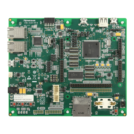
RX71M Group
32
32
RENESAS MCU
RX Family / RX700 Series
All information contained in these materials, including products and product specifications, represents
information on the product at the time of publication and is subject to change by Renesas Electronics
Corporation without notice. Please review the latest information published by Renesas Electronics
Corporation through various means, including the Renesas Electronics Corporation website
(http://www.renesas.com).
Renesas Starter Kit+ User's Manual
Rev. 1.00 Jan 2015
Advertisement
Table of Contents

Related Manuals for Renesas RX71M Series


Summary of Contents for Renesas RX71M Series
- Page 1 All information contained in these materials, including products and product specifications, represents information on the product at the time of publication and is subject to change by Renesas Electronics Corporation without notice. Please review the latest information published by Renesas Electronics Corporation through various means, including the Renesas Electronics Corporation website (http://www.renesas.com).
- Page 2 Electronics product for any application for which it is not intended. Renesas Electronics shall not be in any way liable for any damages or losses incurred by you or third parties arising from the use of any Renesas Electronics product for which the product is not intended by Renesas Electronics.
- Page 3 After use the equipment cannot be disposed of as household waste, and the WEEE must be treated, recycled and disposed of in an environmentally sound manner. Renesas Electronics Europe GmbH can take back end of life equipment, register for this service at http://www.renesas.eu/weee EETS-CD-0098-1.0...
- Page 4 The following documents apply to the RSK+RX71M. Make sure to refer to the latest versions of these documents. The newest versions of the documents listed may be obtained from the Renesas Electronics Web site. Document Type...
- Page 5 Central Processing Unit Cyclic Redundancy Check Digital-to-Analog Converter Dual In-line Package Direct Memory Access DMAC Direct Memory Access Controller Renesas On-chip Debugging Emulator EEPROM Electronically Erasable Programmable Read Only Memory Electromagnetic Compatibility Electrostatic Discharge General PWM Timer C (IIC) Philips™ Inter-Integrated Circuit Connection Bus...
-
Page 6: Table Of Contents
5.10 Universal Serial Bus (USB) ........................23 5.11 LCD Direct Drive Header (TFT) ....................... 24 5.12 External Bus ............................. 25 5.13 Renesas Serial Peripheral Interface (RSPI) .................... 25 5.14 Quad Serial Peripheral Interface (QSPI) ....................25 5.15 I C Bus (Inter-IC Bus) ..........................25 5.16 SD Host Interface (SDHI) ......................... - Page 7 6.19 RSPI Configuration ..........................54 6.20 SDHI Configuration ..........................55 6.21 Serial & USB to Serial Configuration ....................... 56 6.22 SSI Configuration ............................. 57 6.23 USB Configuration ........................... 58 7. Headers ........................... 60 Application Headers ..........................60 Generic Headers ............................65 8.
-
Page 8: Overview
Jan 23, 2015 1. Overview Purpose This RSK+ is an evaluation tool for Renesas microcontrollers. This manual describes the technical details of the RSK+ hardware. The Quick Start Guide and Tutorial Manual provide details of the software installation and debugging environment. -
Page 9: Board Specification
RSK+RX71M 1. Overview Board specification Board specification was shown in Table 1-1 below. Specification Item Part No : R5F571MLCDFC Microcontroller Package : 176-pin LQFP On-Chip Memory : ROM 4MB+64KB, RAM 512KB+32KB+8KB SDRAM : 128Mbit On-Board Memory C EEPROM : 16Kbit SPI Serial Flash : 32Mbit x 2 RX71M Main : 24MHz RX71M Sub : 32.768kHz... -
Page 10: Power Supply
Power-Up Behaviour When the RSK+ is purchased, the RSK+ board has the 'Release' build of the example tutorial software pre- programmed into the Renesas microcontroller. Please consult the 'Renesas Starter Kit+ Code Generator Tutorial Manual' for further information of this example.. -
Page 11: Board Layout
RSK+RX71M 3. Board Layout 3. Board Layout Component Layout Figure 3-1 below shows the top component layout of the board. Application Board Interfaces (Application Headers) Pmod Connector USB0 USBA USB0 Host(RX) Function(RX) Function(RX) Ethernet Status LEDs PMOD1 Ethernet USBA Host(RX) * Reverse ETHERNET1 Connector Serial Flash (RSPI) -
Page 12: Board Dimensions
RSK+RX71M 3. Board Layout Board Dimensions Figure 3-2 below gives the board dimensions and connector positions. All the through-hole connectors are on a common 0.1 inch grid for easy interfacing. Corners x 4 3.0 mm radius USBA Host (Reverse) PMOD1 ETHERNET1 (Ethernet Connector) PHY IC... -
Page 13: Component Placement
RSK+RX71M 3. Board Layout Component Placement Figure 3-3 below shows placement of individual components on the top-side PCB – bottom-side component placement can be seen in Figure 3-4. Component types and values can be looked up using the board schematics. R309 R308 R220... - Page 14 RSK+RX71M 3. Board Layout C118 R463 R477 R478 R464 R479 R465 R480 R466 R481 R467 R482 R468 R483 R484 R329 R343 R455 R358 R344 R456 R396 R469 R457 R397 R470 R458 R398 R399 R471 R459 R381 R440 R473 R460 R382 R441 R429 R442...
-
Page 15: Connectivity
RSK+RX71M 4. Connectivity 4. Connectivity Internal RSK+ Connections The diagram below shows the RSK+ board components and their connectivity to the MCU. DC PWR IN (5V) USB to Serial Regulator IC VBUS 5V Application Board Interface RL78/G1C (Application Header) E1 Debug Interface Function LCD Direct Drive Header (TFT) USB0 (Function/Host) -
Page 16: Debugger Connections
RSK+RX71M 4. Connectivity Debugger Connections The diagram below shows the connections between the RSK+, E1 debugger and the host PC. 5V External Power LCD Display User Interface Cable USB Cable E1 Emulator CPU Board Host PC Figure 4-2: Debugger Connection Diagram R20UT3217EG0100 Rev. -
Page 17: User Circuitry
RSK+RX71M User Circuitry 5. User Circuitry Reset Circuit A reset control circuit is fitted to the RSK+ to generate a reset signal from the RES switch. Refer to the RX71M Group User’s Manual: Hardware for details regarding the reset signal timing requirements, and the RSK+ schematics for information regarding the reset circuitry in use on the board. -
Page 18: Leds
RSK+RX71M User Circuitry LEDs There are 12 LEDs on the RSK+ board. The function of each LED, its color, and its connections are shown in Table 5-3. Color Function Port 3V3_PWR Green Indicates the status of the Board_3V3 power rail. 5V_PWR Green Indicates the status of the Board_5V power rail. -
Page 19: Pmod
RSK+RX71M User Circuitry Pmod™ A Pmod™ Compatible debug LCD module is supplied with the RSK+ board, and should be connected to the PMOD1 header. Care should be taken when installing the LCD module to ensure pins are not bent or damaged. The LCD module is vulnerable to electrostatic discharge (ESD);... -
Page 20: Usb Serial Port
User Circuitry USB Serial Port A USB serial port implemented in another Renesas low power microcontroller (RL78/G1C) is fitted on the RX71M Serial Communications Interface (SCI) module. Multiple options are provided to allow the selection of the connected SCI7 port. Connections between the USB to Serial converter and the microcontroller are listed in Table 5-6 below. -
Page 21: Ethernet
User Circuitry Ethernet When running any Ethernet software, a unique MAC address should be used. A unique Renesas allocated MAC address is attached to the RSK+RX71M PCB as a sticker, and should be always be used with this device ensured to ensure full compatibility when using other Renesas hardware on a common Ethernet connection. - Page 22 RSK+RX71M User Circuitry Ethernet signal Function Port ET1MDIO Management data serial I/O ET1MDC Management serial clock ET1TXCLK Transmit clock ET1TXEN_RMII1TXDEN Transmit enable. ET1TXER* Transmit error. ET1ETXD0_RMII1TXD0 Transmit data bit 0. ET1ETXD1_RMII1TXD1 Transmit data bit 1. ET1ETXD2 Transmit data bit 2. ET1ETXD3 Transmit data bit 3.
-
Page 23: Universal Serial Bus (Usb)
RSK+RX71M User Circuitry 5.10 Universal Serial Bus (USB) This RSK+ board is fitted with a USB host socket (type A) and a function socket (type Mini B). USB module USB0 is connected to the host and function socket, and can operate as either a host or function device. USB module USBA is connected to the host and function socket, and can operate as either a host or function device. -
Page 24: Lcd Direct Drive Header (Tft)
LCD Direct Drive Header (TFT) This RSK+ board is fitted with a LCD Direct Drive thru-hole pattern, which allows connection to compatible Renesas LCD application boards. The pin connections of this header are listed in Table 5-12 below. LCD Direct Drive Header (TFT) -
Page 25: External Bus
Table 5-13: External Bus Address Space 5.13 Renesas Serial Peripheral Interface (RSPI) The RX71M features one Renesas Serial Peripheral Interface modules (Renesas SPI or RSPI). Table 5-14 below details the connected devices, and their connections to the MCU. Slave Select... -
Page 26: Sd Host Interface (Sdhi)
RSK+RX71M User Circuitry 5.16 SD Host Interface (SDHI) A SD Card Slot is fitted to the RSK+ board, and connected to the SD Host Interface (SDHI) MCU peripheral. For further details regarding the SDHI operation, please refer to the RX71M Group User’s Manual: Hardware. The connections for the SDHI signals are listed in Table 5-16 below. -
Page 27: Serial Sound Interface (Ssi)
RSK+RX71M User Circuitry 5.18 Serial Sound Interface (SSI) This RSK+ board is fitted with a Serial Sound Interface (SSI) thru-hole pattern. The connections for the SSI signals are listed in Table 5-18 below. SSI Header (J25) Circuit Net Name Circuit Net Name Port Port Board_5V... -
Page 28: Configuration
RSK+RX71M Configuration 6. Configuration Modifying the RSK+ This section lists the option links that are used to modify the way RSK+ operates in order to access different configurations. Configurations are made by modifying link resistors or headers with movable jumpers or by configuration DIP switches A link resistor is a 0Ω... -
Page 29: E1 Debugger Configuration
RSK+RX71M Configuration E1 Debugger Configuration Table 6-2 below details the function of the option links associated with E1 Debugger configuration. MCU Peripheral Selection Destination Selection Signal name Interface Signal Function MISOA-A J11.Pin1-2 U7.2 J11.Pin2-3, ET0COL SW6.4.OFF U6.3 ET0COL_MISOA-A_PC7 SW6.3.ON J11.Pin2-3, SW4.2 SW6.3.OFF SW6.4.ON... -
Page 30: Power Supply Configuration
RSK+RX71M Configuration Power Supply Configuration Table 6-4 below details the function of the option links associated with power supply configuration. MCU Peripheral Selection Destination Selection Reference Function Interface Function J1.Pin2-3, Connects VBUS0 to 5V Power rail. R221 J23.Pin2-3, R222 VBUS0, VBUSA J4.Pin2-3, Connects VBUSA to 5V Power rail. -
Page 31: Analog Power & Adc & Dac Configuration
RSK+RX71M Configuration Analog Power & ADC & DAC Configuration Table 6-7 below details the function of the option links associated with ADC & DAC configuration. MCU Peripheral Selection Destination Selection Signal name Signal Interface Function R463 JA1.9 R208 R216, R437 (Direct Input via JA1.9) AN000 AN000... -
Page 32: Bus & Sdram Configuration
RSK+RX71M Configuration BUS & SDRAM Configuration Table 6-8 to Table 6-11 below details the function of the option links associated with BUS & SDRAM configuration. MCU Peripheral Selection Destination Selection Signal name Interface Signal Function U3.2 USBAOVRCURA R362 R76, R480 U4.5 USBAOVRCURA_ALE_MTIC5W 68 R76,... - Page 33 RSK+RX71M Configuration MCU Peripheral Selection Destination Selection Signal name Interface Signal Function U12.38 R446 SDCLK SDCLK R380 JA3.44 R445 R358 ET0ERXD1_RMII SW6.7.ON SW6.8.OFF U6.5 0RXD1 ET0ERXD1_RMII0RXD1_CS4n CS4n SW6.8.ON SW6.7.OFF JA3.27 R247 R340 JA3.1 A0_MTIOC6D MTIOC6D R340 R247 JA5.20 R421 R377 U12.23, JA3.2 A1_MTIOC7B MTIOC7B...
- Page 34 RSK+RX71M Configuration MCU Peripheral Selection Destination Selection Signal name Interface Signal Function A19_ET0TXER_QIO0- JA3.40 A_MTIOC4D SW5.7.OFF, ET0TXER SW5.6.ON JA3.40, T26 SW5.8.OFF SW5.6.OFF, A19_ET0TXER_QIO0- BD_QIO0-A SW5.7.ON, R375 SW5.8.OFF, JA3.40, U8.5 A_MTIOC4D R374 SW5.6.OFF, TFT_QIO0-A SW5.7.ON, R374 SW5.8.OFF, JA3.40, TFT.31 R234 R375 SW5.6.OFF, MTIOC4D SW5.8.ON...
- Page 35 RSK+RX71M Configuration MCU Peripheral Selection Destination Selection Signal name Interface Signal Function U12.11, JA3.23, SW8.9.ON SW8.10.OFF TFT.13 D6_SDHID0-B SDHID0-B SW8.10.ON SW8.9.OFF SD1.7 U12.13, JA3.24, SW9.1.ON SW9.2.OFF TFT.14 D7_SDHID1-B SDHID1-B SW9.2.ON SW9.1.OFF SD1.8 U12.42, JA3.29, R442 R405 TFT.15 D8_IO0 R405 R442 JA1.15 U12.44, JA3.30, R441...
-
Page 36: Can Configuration
RSK+RX71M Configuration CAN Configuration Table 6-12 below details the function of the option links associated with CAN configuration. MCU Peripheral Selection Destination Selection Signal name Interface Signal Function VSYNC R269 J15.Open J26.9 U11.1 R211 CTX0 J15.Pin1-2 R269 JA5.5 CTX0_VSYNC_MTIOC0C_IRQ2-DS R90, JA2.23 R154 R153... - Page 37 RSK+RX71M Configuration MCU Peripheral Selection Destination Selection Signal name Interface Signal Function YINPUT1 R239 R133 TFT.44 AN005_YINPUT1_P45 167 P45 AN005 R133 R239, R427 JA5.2 R427 R133 PMOD1.1 R426 XINPUT2 R240 R130 TFT.45 AN006_XINPUT2_P46 166 P46 AN006 R130 R240, R315 JA5.3 R315 R130 PMOD1.9...
- Page 38 RSK+RX71M Configuration MCU Peripheral Selection Destination Selection Signal name Interface Signal Function U12.2, JA3.17, TFT.7 U12.4, JA3.18, TFT.8 U12.5, JA3.19, SW8.1.ON SW8.2.OFF TFT.9 D2_SDHID2-B SDHID2-B SW8.2.ON SW8.1.OFF SD1.9 U12.7, JA3.20, SW8.3.ON SW8.4.OFF TFT.10 D3_SDHID3-B SDHID3-B SW8.4.ON SW8.3.OFF SD1.1 U12.8, JA3.21, SW8.5.ON SW8.6.OFF TFT.11...
-
Page 39: Ethernet Configuration
RSK+RX71M Configuration MCU Peripheral Selection Destination Selection Signal name Interface Signal Function U12.50, JA3.34, R228 R390 TFT.20 D13_IO5 R390 R228 JA1.20 SW9.4.OFF, SW9.5.OFF, U12.51, JA3.35, SW9.3.ON SW9.6.OFF TFT.21 SW9.3.OFF, SW9.5.OFF, SDHICD-B SW9.4.ON SD1.10 SW9.6.OFF D14_SDHICD- B_MTIOC6C_IO6 SW9.3.OFF, SW9.4.OFF, MTIOC6C SW9.5.ON JA5.11 SW9.6.OFF SW9.3.OFF,... - Page 40 RSK+RX71M Configuration MCU Peripheral Selection Destination Selection Signal name Interface Signal Function SW7.2.OFF, ET0TXEN_RMII0TXDEN SW7.1.ON U6.13 SW7.3.OFF ET0TXEN_RMII0TXDEN_QIO2- SW7.1.OFF, QIO2-A SW7.2.ON U8.3 SW7.3.OFF A_MTIOC3B SW7.1.OFF, MTIOC3B SW7.3.ON JA2.13 SW7.2.OFF SW7.5.OFF, ET0ETXD0_RMII0TXD0 SW7.4.ON U6.14 SW7.6.OFF ET0ETXD0_RMII0TXD0_QIO3- SW7.4.OFF, QIO3-A SW7.5.ON U8.7 SW7.6.OFF A_MTIOC3D SW7.4.OFF, MTIOC3D...
- Page 41 RSK+RX71M Configuration MCU Peripheral Selection Destination Selection Signal name Interface Signal Function A20_ET0TXCLK_QIO1- R345 JA3.41 A_POE0n R345, SW5.10.OF ET0TXCLK JA3.41, U6.12 SW5.9.ON R345, SW5.9.OFF, BD_QIO1-A SW5.10.ON JA3.41, U8.2 A20_ET0TXCLK_QIO1- R370, R372 R371 A_POE0n R345, SW5.9.OFF, TFT_QIO1-A SW5.10.ON JA3.41, TFT.30 R225 R371, R372 , R370...
-
Page 42: General Io & Led Configuration
RSK+RX71M Configuration MCU Peripheral Selection Destination Selection Signal name Interface Signal Function ET1CRS_RMII1CRSDV J18.Pin1-2 U6.61 R158, R159, J18.Pin2-3, U10.3 R171 A-RXD7 R415 R164 ET1CRS_RMII1CRSDV_A- R172 RXD7_P-RXD7 JA2.8 J18.Pin2-3, P-RXD7 R172 PMOD2.3 R415 U6.43, ET1LINKSTA R407 R191, R408 ETHERNE ET1LINKSTA_A- T1.11 CTS7RTS7_P-CTS7RTS7 R408 A-CTS7RTS7... - Page 43 RSK+RX71M Configuration MCU Peripheral Selection Destination Selection Signal name Signal Interface Function SW9.4.OFF, U12.51, JA3.35, SW9.3.ON SW9.5.OFF, TFT.21 SW9.6.OFF SW9.3.OFF, SDHICD-B SW9.4.ON SW9.5.OFF, SD1.10 SW9.6.OFF D14_SDHICD- B_MTIOC6C_IO6 SW9.3.OFF, SW9.4.OFF, MTIOC6C SW9.5.ON JA5.11 SW9.6.OFF SW9.3.OFF, SW9.4.OFF, SW9.6.ON JA1.21 SW9.5.OFF SW9.8.OFF, U12.53, JA3.36, SW9.7.ON SW9.9.OFF,...
-
Page 44: I2C & Eeprom Configuration
RSK+RX71M Configuration 6.12 I2C & EEPROM Configuration Table 6-24 and Table 6-25 below detail the function of the option links associated with I2C & EEPROM configuration. MCU Peripheral Selection Destination Selection Signal name Interface Signal Function TXD6 R119 PMOD1.2 TXD6_SSDA6 SSDA6 R118 J26.19... -
Page 45: Mtu & Tpu & Poe Configuration
RSK+RX71M Configuration 6.13 MTU & TPU & POE Configuration Table 6-26 to Table 6-29 below details the function of the option links associated with MTU & TPU & POE configuration. MCU Peripheral Selection Destination Selection Signal name Interface Signal Function U3.2 USBAOVRCURA R362 R76, R480... - Page 46 RSK+RX71M Configuration MCU Peripheral Selection Destination Selection Signal name Interface Signal Function R72, R327 AUDIOMCLK R289 R270, J25.5 USBAOVRCURB_AUDIOMCL USBAOVRCURB R327 R72, R270, R289 U4.6 K_PIXD6_MTCLKC PIXD6 R270 R72, R289, R327 J26.12 MTCLKC R270, R289, R327 JA5.17 SSISCK0 R291 R271, R342 J25.9 PIXD7...
- Page 47 RSK+RX71M Configuration MCU Peripheral Selection Destination Selection Signal name Interface Signal Function ET0ETXD1_RMII0T SW7.7.ON SW7.8.OFF U6.15 ET0ETXD1_RMII0TXD1_MTIO EDREQ1 SW7.8.ON, R231 SW7.7.OFF, R455 JA6.1, TFT28 C4A_EDREQ1 MTIOC4A SW7.8.ON, R455 SW7.7.OFF, R231 JA2.15 ET0CRS_RMII0CR SW7.9.ON SW7.10.OFF U6.1 ET0CRS_RMII0CRSDV_MTIO C4C_EDACK1 EDACK1 SW7.10.ON, R229 SW7.9.OFF, R456 JA6.2, TFT23...
- Page 48 RSK+RX71M Configuration MCU Peripheral Selection Destination Selection Signal name Interface Signal Function A20_ET0TXCLK_QIO1 R345 JA3.41 -A_POE0n R345, ET0TXCLK SW5.10.OFF JA3.41, U6.12 SW5.9.ON R345, SW5.9.OFF, BD_QIO1-A SW5.10.ON, JA3.41, U8.2 A20_ET0TXCLK_QIO1- R370, R372 R371 A_POE0n R345, SW5.9.OFF, R225 TFT_QIO1-A SW5.10.ON, JA3.41, TFT.30 R371, R372 R370...
-
Page 49: Irq & Nmi & Switch Configuration
RSK+RX71M Configuration 6.14 IRQ & NMI & Switch Configuration Table 6-30 below details the function of the option links associated with IRQ & NMI & Switch configuration. MCU Peripheral Selection Destination Selection Signal name Interface Signal Function R492 ADTRG0n ADTRG0n JA1.8 JA5.12 MTIC5U... -
Page 50: Pdc Configuration
RSK+RX71M Configuration 6.15 PDC Configuration Table 6-31 and Table 6-32 below details the function of the option links associated with PDC configuration. MCU Peripheral Selection Destination Selection Signal name Interface Signal Function TXD6 R119 PMOD1.2 TXD6_SSDA6 SSDA6 R118 J26.19 R307 RXD6 R128 PMOD1.3... -
Page 51: Pmod1 Configuration
RSK+RX71M Configuration 6.16 PMOD1 Configuration Table 6-33 below details the function of the option links associated with PMOD1 Interface configuration. MCU Peripheral Selection Destination Selection Signal name Interface Signal Function TXD6 R119 PMOD1.2 TXD6_SSDA6 SSDA6 R118 J26.19 R307 RXD6 R128 PMOD1.3 RXD6_SSCL6 SSCL6... -
Page 52: Pmod2 Configuration
RSK+RX71M Configuration 6.17 PMOD2 Configuration Table 6-34 below details the function of the option links associated with PMOD2 Interface configuration. MCU Peripheral Selection Destination Selection Signal name Interface Signal Function AN002 R203 R179 JA1.11 AN002_IRQ10-DS IRQ10-DS R179 R203 PMOD2.7 AN003 R202 R176 JA1.12... -
Page 53: Qspi Configuration
RSK+RX71M Configuration 6.18 QSPI Configuration Table 6-35 below details the function of the option links associated with QSPI configuration. MCU Peripheral Selection Destination Selection Signal name Interface Signal Function J8.Pin1-2, R26, R64, REF50CK0 U6.70, X5.3 R62, R63 J8.Pin1-2, ET0RXCLK U6.79 ET0RXCLK_REF50CK0_QSSL-A J8.Pin2-3, R392... -
Page 54: Rspi Configuration
RSK+RX71M Configuration 6.19 RSPI Configuration Table 6-36 below details the function of the option links associated with RSPI configuration. MCU Peripheral Selection Destination Selection Signal name Interface Signal Function SSLA1-A J10.Pin1-2 U7.1 A16_ET0ERXD3 J10.Pin2-3 JA3.37 A16_ET0ERXD3_SSLA1-A J10.Pin2-3, ET0ERXD3 JA3.37, U6.9 SW5.1.ON RSPCKA-A J12.Pin1-2... -
Page 55: Sdhi Configuration
RSK+RX71M Configuration 6.20 SDHI Configuration Table 6-37 below details the function of the option links associated with SD Host Interface configuration. MCU Peripheral Selection Destination Selection Signal name Interface Signal Function U12.5, JA3.19, SW8.1.ON SW8.2.OFF TFT.9 D2_SDHID2-B SDHID2-B SW8.2.ON SW8.1.OFF SD1.9 U12.7, JA3.20,... -
Page 56: Serial & Usb To Serial Configuration
RSK+RX71M Configuration 6.21 Serial & USB to Serial Configuration Table 6-38 below details the function of the option links associated with Serial & USB to Serial configuration. MCU Peripheral Selection Destination Selection Signal name Interface Signal Function R419 AN001 R207 R237, JA1.10 AN001_RXCTS_YDRIVE... -
Page 57: Ssi Configuration
RSK+RX71M Configuration 6.22 SSI Configuration Table 6-39 below details the function of the option links associated with Serial Sound Interface configuration. MCU Peripheral Selection Destination Selection Signal name Interface Signal Function SSITXD0 R292 R192, R275 J25.12 R292 PIXD3 R275 R192, J26.15 SSITXD0_PIXD3_SDA2-DS 46 P17... -
Page 58: Usb Configuration
RSK+RX71M Configuration 6.23 USB Configuration Table 6-40 and Table 6-41 below details the function of the option links associated with the USB Configuration. MCU Peripheral Selection Destination Selection Signal name Interface Signal Function U3.2 USBAOVRCURA R362 R76, R480 U4.5 USBAOVRCURA_ALE_MTIC5W R76, R466 R447... - Page 59 RSK+RX71M Configuration MCU Peripheral Selection Destination Selection Reference Interface Function Function Enables Self-powered. USB0VBUS Enables Bus-powered. Sets current limit as 0.7A. U3.4 ILIM Sets current limit as 1.95A. U3.4 VBUSA Enables USBA OTG mode. J4.Open U4.1 Connects VBUSA to J23.3 R221 R222 J23.3...
-
Page 60: Headers
7. Headers Application Headers This RSK+ board is fitted with application headers, which can be used to connect compatible Renesas application devices or as easy access to MCU pins. Table 7-1 below lists the connections of the application header, JA1. - Page 61 RSK+RX71M 7. Headers Table 7-2 below lists the connections of the application header, JA2. Application Header JA2 Function Function MCU Pin MCU Pin Circuit Net Name Circuit Net Name RESET EXTAL RESn CON_EXTAL Vss1 GROUND WDT_OVF SCIaTX A-TXD7 IRQ0 / WKUP / M1_HSIN0 SCIaRX 27 / NC / 27 MTIOC0A_IRQ4...
- Page 62 RSK+RX71M 7. Headers Table 7-3 below lists the connections of the BUS application header, JA3. Application Header JA3 (Bus) Function Function MCU Pin MCU Pin Circuit Net Name Circuit Net Name WR / SDWE 72 / 136 WRn / WEn CS4n CON_SDCSn A16_ET0ERXD3...
- Page 63 RSK+RX71M 7. Headers Table 7-4 below lists the connections of the application header, JA5. Application Header JA5 Function Function MCU Pin MCU Pin Circuit Net Name Circuit Net Name ADC4 ADC5 AN004 AN005 ADC6 ADC7 AN006 AN007 CAN1TX CAN1RX CTX0 CRX0 CAN2TX CAN2RX...
- Page 64 RSK+RX71M 7. Headers Table 7-5 below lists the connections of the application header, JA6. Application Header JA6 Function Function MCU Pin MCU Pin Circuit Net Name Circuit Net Name DREQ DACK EDREQ1 EDACK1 TEND STBYn RS232TX RS232RX RS232TX RS232RX SCIbRX SCIbTX RXD1 TXD1...
-
Page 65: Generic Headers
RSK+RX71M 7. Headers Generic Headers Generic headers, used to provide easy connections to various pins from devices fitted to the RSK+. Table 7-6 below lists the connections of the LCD Direct Drive (TFT) Header. LCD Direct Drive Header (TFT) Header Name Header Name MCU Pin MCU Pin... -
Page 66: Code Development
8. Code Development Overview For all code debugging using Renesas software tools, the RSK+ board must be connected to a PC via an E1/E20 debugger. An E1 debugger is supplied with this RSK+ product. For further information regarding the debugging capabilities of the E1/E20 debuggers, refer to E1/E20 Emulator Additional Document for User's Manual (R20UT0399EJ). -
Page 67: Additional Information
Copyright This document may be, wholly or partially, subject to change without notice. All rights reserved. Duplication of this document, either in whole or part is prohibited without the written permission of Renesas Electronics Europe Limited. © 2015 Renesas Electronics Europe Limited. All rights reserved. - Page 68 REVISION HISTORY RSK+RX71M User’s Manual Rev. Date Description Page Summary 1.00 Jan 23, 2015 First Edition issued...
- Page 69 Renesas Starter Kit+ Manual: User’s Manual Publication Date: Rev. 1.00 Jan 23, 2015 Published by: Renesas Electronics Corporation...
- Page 70 SALES OFFICES Refer to "http://www.renesas.com/" for the latest and detailed information. Renesas Electronics America Inc. 2801 Scott Boulevard Santa Clara, CA 95050-2549, U.S.A. Tel: +1-408-588-6000, Fax: +1-408-588-6130 Renesas Electronics Canada Limited 9251 Yonge Street, Suite 8309 Richmond Hill, Ontario Canada L4C 9T3...
- Page 71 RX71M Group R20UT3217EG0100...
- Page 72 Mouser Electronics Authorized Distributor Click to View Pricing, Inventory, Delivery & Lifecycle Information: Renesas Electronics YRPBRX71M...
Need help?
Do you have a question about the RX71M Series and is the answer not in the manual?
Questions and answers