Table of Contents
Advertisement
Quick Links
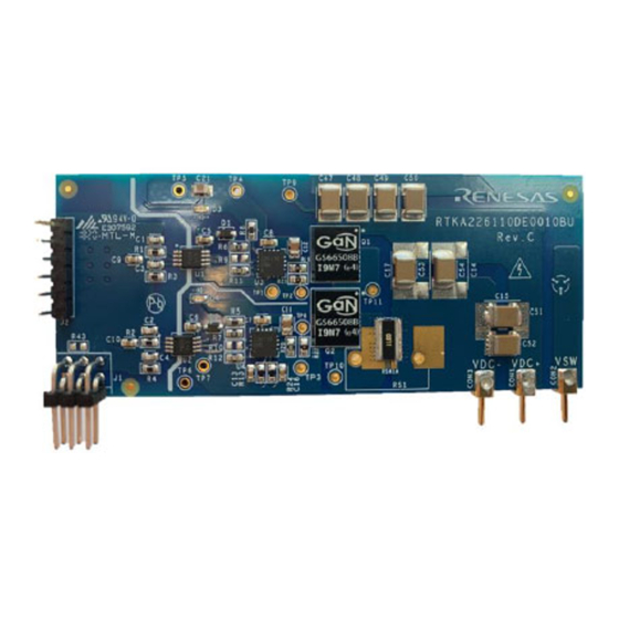
RTKA226110DE0010BU
Evaluation Board
This user manual discusses the RTKA226110DE0010BU with GS66508B GaN E-HEMT daughter board and
GS665MB-EVB evaluation platform. The RTKA226110DE0010BU is a gate drive evaluation board following the
GS665XXX-EVBDB daughter board style and uses the RAA226110 device. This evaluation board consists of two
GaN Systems 650V GaN Enhancement-mode HEMTs (E-HEMTs) and all necessary circuits including half-bridge
gate drivers, isolated power supplies, and an optional heatsink to form a functional half-bridge power stage. It
allows you to evaluate the GaN E-HEMT performance in any half-bridge-based topology, either with the universal
mother board (GS665MB-EVB) or your own system design. The RTKA226110DE0010BU evaluation board
provides a 0V turn-off voltage solution. A 0V turn-off solution is normally used in low power applications. A 0V
turn-off solution is easy to implement as there is no need for a negative power supply rail and the reverse
conduction voltage drop of GaN is lower. For the E-mode GaN device, the V
1.7V). A 0V turn-off has the risk of false turn-on when the GaN device is in an off state. Also, the switching-off loss
is higher than the negative turn-off voltage. The 0V turn-off solution is normally used in low power applications.
Read the entire user manual and, specifically, the warnings and restrictions notices before handling the product.
Persons handling the product(s) must have electronics training and observe good engineering practice standards.
Features
• Serves as a reference design and evaluation tool in addition to a deployment-ready solution for easy in-system
evaluation.
• Vertical mount style with the height of 35mm that fits in the majority of 1U designs and allows evaluation of a
GaN E-HEMT in traditional through-hole type power supply board.
• Current shunt position for switching characterization testing
• Universal form factor and footprint for all products
• 0V turn off voltage
Related Literature
For a full list of related documents, visit our website:
•
RAA226110
device page
Ordering Information
Part Number
RTKA226110DE0010BU
DANGER!
This evaluation board is designed for engineering evaluation in a controlled lab environment and should be handled by
qualified personnel ONLY. High voltage is exposed on the board during the test and even brief contact during operation
may result in severe injury or death.
Never leave the board operating unattended. After it is de-energized, always wait until all capacitors are discharged
before touching the board.
CAUTION:
This product contains parts that are susceptible to damage by Electrostatic Discharge (ESD). Always follow ESD
prevention procedures when handling the product.
X0115710 Rev.1.00
Dec.7.20
RAA226110 evaluation board
User Manual
threshold voltage is low (typical
GS
Description
Page 1 of 25
Advertisement
Table of Contents

Related Manuals for Renesas RAA226110


Summary of Contents for Renesas RAA226110
- Page 1 GS665MB-EVB evaluation platform. The RTKA226110DE0010BU is a gate drive evaluation board following the GS665XXX-EVBDB daughter board style and uses the RAA226110 device. This evaluation board consists of two GaN Systems 650V GaN Enhancement-mode HEMTs (E-HEMTs) and all necessary circuits including half-bridge gate drivers, isolated power supplies, and an optional heatsink to form a functional half-bridge power stage.
- Page 2 RTKA226110DE0010BU ENABLE Iso. DC/DC PWMH VDC+ Isolator RAA226110 PWML IL611-1E Gate Driver Iso. DC/DC C4-10 Isolator RAA226110 IL611-1E Gate Driver Shunt VDC- Figure 1. RTKA226110DE0010BU Evaluation Board Block Diagram X0115710 Rev.1.00 Page 2 of 25 Dec.7.20...
-
Page 3: Functional Description
RTKA226110DE0010BU 1. Functional Description Functional Description Control and Power I/Os: The daughter board RTKA226110DE0010BU circuit diagram is shown in Figure 1. The control logic inputs on the 2x3 pin header J1 are listed in Table Table 1. Control Pins Description ENABLE Enable input. - Page 4 RTKA226110DE0010BU 1. Functional Description The universal 650V mother board evaluation kit includes the following items: • Mother board GS665MB-EVB • 12V 1.2.1 12V Input The mother board can be powered by 9V to 12V on J1. The on-board voltage regulator creates 5V for the daughter board and control logic circuits.
-
Page 5: Test Points
An external power inductor (not included) can be connected between VSW (CON1) and VOUT (CON4/5) or VDC+ (CON2/3) for double pulse test. You can choose your inductor size to meet the test requirement. Renesas recommends using a power inductor with low inter-winding capacitance to obtain best switching performance. For the double pulse testing, use 2x 60µH/40A inductor (CWS, HF467-600M-40AV) in series. -
Page 6: Buck/Standard Half-Bridge Mode
The double pulse signal can be generated using a programmable signal generator or microcontroller/DSP board. Because this test involves high switching stress and high current, Renesas recommends setting the double pulse test gate signal as a single trigger mode or use a long repetition period (for example >50ms-100ms) to avoid excess stress to the switches. - Page 7 RTKA226110DE0010BU 1. Functional Description Using RTKA226110DE0010BU in System The daughter board allows you to evaluate the GaN performance in your own systems. See the footprint drawing of RTKA226110DE0010BU shown in Figure 1 3 5 2 4 6 1. All units are in mm. 2.
- Page 8 RTKA226110DE0010BU 1. Functional Description f. Connect an external inductor between CON1 and CON3. Use the current probe to measure the inductor current (I 4. Set up and check the PWM gate signal a. Turn on the 12V power. b. Check the two LEDs on the daughter board. They should be turned on indicating the isolated 9V is present. c.
-
Page 9: Test Results
RTKA226110DE0010BU 1. Functional Description Test Results Pulses test (V = 400V, IMAX = 33A, Lp = 120µH, R = 0Ω, IGSEL is connected to VDRV, Gate driver G(ON) current is 0.3A, R =1Ω, 8 pulses, period = 4µs, duty = 50%). G(OFF) Vds_low-side I_inductor... - Page 10 RTKA226110DE0010BU 1. Functional Description Synchronous Buck Test (L = 120µH, V = 400V, V = 80V, D = 20%, f = 100kHz, POUT = 300W). V_out Vds_low-side I_inductor PWM_low-side Figure 9. Buck Test Waveform (POUT = 300W) X0115710 Rev.1.00 Page 10 of 25 Dec.7.20...
-
Page 11: Pcb Layout Guidelines
• A. 2x GaN Systems 650V E-HEMT GS66508B, 30A/50mΩ • B. Decoupling capacitors C14-C17 and C47-C54 • C. Signal isolator IL611-1E • D. GaN driver RAA226110 • E. OCP shunt • F. TP8 (gate) and TP3 (source) test points for bottom Q2 V •... -
Page 12: Gate Driver Circuit
Gate Driver Circuit The Renesas RAA226110 low-side gate driver is chosen for this design. This driver provides 5.8V gate drive with 3.8V UVLO. It supports the 5.8V turn-on and -3V/0V turn-off. It has separated source and sink drive outputs that eliminates the need for an additional diode. - Page 13 Eon/Eoff measurement. • The current shunt also provides the OCP signal for the RAA226110 to trigger OCP. The OCP threshold voltage 40mV/80mV/120mV can be configured through the IDSET pin of RAA226110.
-
Page 14: Thermal Design
RTKA226110DE0010BU 2. PCB Layout Guidelines 2.1.6 Thermal Design • GS66508B has a thermal pad on the bottom side for heat dissipation. The heat is transferred to the bottom side of the Printed Circuit Board (PCB) using thermal vias and copper plane. •... - Page 15 RTKA226110DE0010BU Circuit Schematic VDDHIN VDRVH VDRVH VDC+ UNNAMED_5_RAA226110_I441_1 RB751V40 VDRV CON1 OUTH UNNAMED_5_GS66508B_I420_3 UNNAMED_5_RAA226110_I441_10 OUTL 16PF RAA226110 UNNAMED_5_IL611_I227_PIN8 IN1+ VEEL UNNAMED_5_IL611_I227_PIN2 UNNAMED_5_IL611_I227_PIN7 OUT1 IN1- UNNAMED_5_IL611_I227_PIN6 GS66508B PWMH_IN IN2+ OUT2 UNNAMED_5_IL611_I227_PIN4 IN2- IL611-1E UNNAMED_5_RAA226110_I441_5 VDRVH 16PF TP11 HIGH VOLTAGE SECTION HIGH SIDE SECTION...
- Page 16 20mA, 574nm, 35mcd, ROHS U1, U2 IC-DIGITAL ISOLATOR, SMD, 8P, MSOP, IL611-1E 2-CHANNEL, 2500Vrms, ROHS Corporation U3, U4 IC Low-Side Gan Driver, 16P, QFN, 4x4, Renesas RAA2261104GNP#MA0 ROHS Electronics Q1, Q2 TRANSISTOR-MOS, N-CHANNEL, SMD, GaN Systems GS66508B-E01-MR 8.8x7mm, 650V, 30A, 50mΩ, ROHS R9, R10, R43 RESISTOR, SMD, 0603, 0.1%, MF,...
- Page 17 RTKA226110DE0010BU 2. PCB Layout Guidelines Reference Designator Description Manufacturer Manufacturer Part HS1-Cut thermal sheet into 1.378 Instructions for assembly. Renesas Assembly Instructions inch squares and place between Electronics heat sink and PCB. America HS1 (SEE ASSY INSULATION-BOND-PLY, 11mil, 10x10in, Bergquist BP100-0.011-00-1010-NA...
- Page 18 RTKA226110DE0010BU 2. PCB Layout Guidelines Figure 21. Solder Top Figure 22. Top Layer Figure 23. Layer 2 X0115710 Rev.1.00 Page 18 of 25 Dec.7.20...
- Page 19 RTKA226110DE0010BU 2. PCB Layout Guidelines Figure 24. Layer 3 Figure 25. Bottom Layer Figure 26. Solder Bottom X0115710 Rev.1.00 Page 19 of 25 Dec.7.20...
- Page 20 Appendix A - GS665MB-EVB To ensure that you have the latest GS665MB-EVB information, visit the GaN systems Inc website. GS665MB-EVB Circuit Schematics...
-
Page 21: Board Layout
RTKA226110DE0010BU 3. Appendix A - GS665MB-EVB GS665MB-EVB Board Layout Figure 27. Assembly Top Figure 28. Assembly Bottom X0115710 Rev.1.00 Page 21 of 25 Dec.7.20... - Page 22 GS665MB-EVB Bill of Materials Quantity Reference Description Value Manufacturer Part number Assembly Note PCB bare 2-layer 2oz Cu. Gerber file: GS665EVBMB- Shenzhen Sprint GS665EVBMB- GerberNCDrill-RevB- GerberNCDrill-RevB- 20160628 20160628 CON1, CON2, CON3, TERMINAL SCREW VERTICAL PC MNT CON-10-32-SCRWMNT Keystone RevB- DO NOT INSTALL * CON4, CON5, CON6, CON7 CAP ALUM 220µF 20% 25V SMD...
- Page 23 Quantity Reference Description Value Manufacturer Part number Assembly Note TP1, TP2, TP3, TP4, TEST POINT PCB TP-KEYSTONE-5010 KEYSTONE 5010 TP7, TP8, TP9, TP10, TP11, TP12, TP13 TR1, TR2 TRIM POT CERM 2kΩ 25TRN TOP DO NOT INSTALL * COMM MODE CHOKE 5.2A T/H CMC-08 RECOM CMC-08...
-
Page 24: Revision History
RTKA226110DE0010BU 4. Revision History Revision History Rev. Date Description 1.00 Dec.7.20 Initial release X0115710 Rev.1.00 Page 24 of 25 Dec.7.20... -
Page 25: Evaluation Board/Kit Important Notice
If any part of this document refers to any third-party products or services it shall not be deemed a license grant by Renesas for the use of such third-party products or services, or any intellectual property contained therein or considered as a warranty covering the use in any manner whatsoever of such third-party products or services or any intellectual property contained therein. - Page 26 Renesas' products are provided only subject to Renesas' Terms and Conditions of Sale or other applicable terms agreed to in writing. No use of any Renesas resources expands or otherwise alters any applicable warranties or warranty disclaimers for these products.
Need help?
Do you have a question about the RAA226110 and is the answer not in the manual?
Questions and answers