
Related Manuals for Quectel BC660K-GL


Summary of Contents for Quectel BC660K-GL
- Page 1 BC660K-GL Hardware Design NB-IoT Module Series Version: 1.0 Date: 2021-01-12 Status: Released www.quectel.com...
- Page 2 To the maximum extent permitted by law, Quectel excludes all liability for any loss or damage suffered in connection with the use of the functions and features under development, regardless of whether such loss or damage may have been foreseeable.
- Page 3 BC660K-GL Hardware Design Copyright The information contained here is proprietary technical information of Quectel. Transmitting, reproducing, disseminating and editing this document as well as using the content without permission are forbidden. Offenders will be held liable for payment of damages. All rights are reserved in the event of a patent grant or registration of a utility model or design.
-
Page 4: Safety Information
Manufacturers of the cellular terminal should notify users and operating personnel of the following safety information by incorporating these guidelines into all manuals of the product. Otherwise, Quectel assumes no liability for customers’ failure to comply with these precautions. -
Page 5: About The Document
NB-IoT Module Series BC660K-GL Hardware Design About the Document Revision History Version Date Author Description Clifton HE/ 2020-09-30 Ellison WANG/ Creation of the document Randy LI Clifton HE/ 2021-01-12 Ellison WANG/ First official release Randy LI BC660K-GL_Hardware_Design 4 / 57... -
Page 6: Table Of Contents
NB-IoT Module Series BC660K-GL Hardware Design Contents Safety Information ............................3 About the Document ..........................4 Contents ..............................5 Table Index ..............................7 Figure Index ..............................8 Introduction ............................9 Product Concept ..........................10 2.1. General Description ......................... 10 2.2. - Page 7 NB-IoT Module Series BC660K-GL Hardware Design 4.2. Operating Frequency ....................... 35 4.3. RF Antenna Reference Design ....................36 4.4. Reference Design of RF Layout ....................37 4.5. Antenna Requirements ......................38 4.6. RF Output Power ........................39 4.7. RF Receiving Sensitivity ......................40 4.8.
- Page 8 NB-IoT Module Series BC660K-GL Hardware Design Table Index Table 1: Frequency Bands of BC660K-GL ....................10 Table 2: Key Features of BC660K-GL ....................... 11 Table 3: I/O Parameters Definition ......................16 Table 4: Pin Description ..........................16 Table 5: Application Processor (AP) Operating Modes ................20 Table 6: Modem Operating Modes ......................
- Page 9 NB-IoT Module Series BC660K-GL Hardware Design Figure Index Figure 1: Functional Diagram ........................13 Figure 2: Pin Assignment ........................... 15 Figure 3: Module Power Consumption in Different Modem Modes ............21 Figure 4: Timing of Waking Up Module from PSM ..................22 Figure 5: Reference Design for Power Supply ..................
-
Page 10: Introduction
This document provides information on the functional features, interface specifications, as well as electrical and mechanical details of the BC660K-GL module. Consult this document to learn about the air interface, hardware interface, external application reference designs and other related information of the module. -
Page 11: Product Concept
H-FDD B1/B2/B3/B4/B5/B8/B12/B13/B14/B17/B18/B19/B20/B25/B28/B66/B70/B85 BC660K-GL is an SMD type module with LCC and LGA package, and has an ultra-compact profile of 17.7 mm × 15.8 mm × 2.0 mm, which makes it easily embedded into size-constrained applications and provide reliable connectivity with the applications. -
Page 12: Key Features
NB-IoT Module Series BC660K-GL Hardware Design 2.2. Key Features The following table describes the detailed features of BC660K-GL module. Table 2: Key Features of BC660K-GL Item Details ⚫ Supply voltage: 2.2–4.3 V Power Supply ⚫ Typical supply voltage: 3.3 V... -
Page 13: Functional Diagram
3GPP. When the temperature returns to the normal operating temperature levels, the module will meet 3GPP specifications again. "*" means under development. 2.3. Functional Diagram The following figure shows a block diagram of BC660K-GL and illustrates the major functional parts. ⚫ RF Transceiver and Subsystem ⚫... -
Page 14: Evaluation Board
Figure 1: Functional Diagram 2.4. Evaluation Board Quectel provides a complete set of development tools to facilitate the use and testing of BC660K-GL module. The development tool kit includes a TE-B board, a micro-USB cable, a rod antenna and other peripherals. -
Page 15: Application Functions And Interfaces
NB-IoT Module Series BC660K-GL Hardware Design Application Functions and Interfaces BC660K-GL is equipped with 58 pins, including 44 LCC pins and 14 LGA pins. The subsequent chapters provide detailed descriptions of the following functions/pins/interfaces: ⚫ Power Supply ⚫ PSM_EINT ⚫... -
Page 16: Pin Assignment
NB-IoT Module Series BC660K-GL Hardware Design 3.1. Pin Assignment ANT_RF RESERVED GPIO1 RESERVED GPIO2 RESERVED GRFC2 GPIO3 RESERVED GPIO4 RESERVED BC660K-GL GRFC1 BOOT RESERVED Top View RESERVED RESERVED ADC0 VIO_SEL USIM_GND RESERVED USIM_DATA RESERVED USIM_RST VDD_EXT USIM_CLK RESERVED Power UART... -
Page 17: Pin Description
NB-IoT Module Series BC660K-GL Hardware Design 3.2. Pin Description Table 3: I/O Parameters Definition Type Description Analog Input Digital Input Digital Output Digital Input/Output Power Input Power Output Table 4: Pin Description Power Supply Pin Name Pin No. Description DC Characteristics Comment Vmax = 4.3 V... - Page 18 NB-IoT Module Series BC660K-GL Hardware Design download mode Reset Interface Pin Name Pin No. Description DC Characteristics Comment max = 0.42 V Reset the RESET_N min = 1.33 V Active low. module max = 2.2 V PSM_EINT Interface Pin Name Pin No.
- Page 19 NB-IoT Module Series BC660K-GL Hardware Design Debug UART max = 0.2 × VDD_EXT DBG_RXD receive min = 0.7 × VDD_EXT VDD_EXT max = 0.15 × VDD_EXT power domain. Debug UART DBG_TXD min = 0.8 × VDD_EXT transmit RI Interface Pin Name Pin No.
-
Page 20: Operating Modes
NB-IoT Module Series BC660K-GL Hardware Design General-purpose GPIO4 input/output GRFC Interfaces* Pin Name Pin No. Description DC Characteristics Comment Generic RF max = 0.27 V 1.8 V power GRFC1 controller min = 1.44 V domain. If unused, keep Generic RF max = 0.27 V... -
Page 21: Power Saving
NB-IoT Module Series BC660K-GL Hardware Design Table 5: Application Processor (AP) Operating Modes Mode Description Normal In normal mode, the AP handles tasks such as AT command communication. Idle When all tasks are suspended, the AP enters idle mode. Table 6: Modem Operating Modes... -
Page 22: Deep Sleep
NB-IoT Module Series BC660K-GL Hardware Design edge of PSM_EINT or by your sending the command AT to it via the main UART port. 3.4.2. Deep Sleep The module consumes extremely low current in Deep Sleep mode (typical value: 800 nA). The main purpose of Deep Sleep is to reduce the power consumption of the module and prolong the power supply duration of the battery. -
Page 23: Power Supply
Power design for a module is critical to its performance. It is recommended to use a low quiescent current LDO with an output capacity of 0.5 A to regulate the power supply for BC660K-GL. Lithium-thionyl chloride (Li-SOCl2) batteries and Lithium manganese oxide (LiMn2O4) batteries can be used as the power supply. -
Page 24: Power Supply Voltage Detection
NB-IoT Module Series BC660K-GL Hardware Design withstanding capability. In principle, the longer the VBAT trace is, the wider it should be. A reference circuit for power supply is illustrated in the following figure. Module VBAT VBAT 100 μF 100 nF 100 pF 22 pF Figure 5: Reference Design for Power Supply 3.5.3. -
Page 25: Turn Off
NB-IoT Module Series BC660K-GL Hardware Design NOTES After the module is powered off, it can be turned on again only after its VBAT voltage drops below 0.7 V. The actual discharging time of VBAT needs to be determined based on circuit tests and enough time margin should be left to avoid abnormal module startup. -
Page 26: Download Mode
NB-IoT Module Series BC660K-GL Hardware Design RESET_N 4.7 kΩ 100 nF Reset pulse 47 kΩ Figure 8: Reference Design for RESET_N Controlled with an OC/OD Driving Circuit RESET_N 100 nF Close to S1 Figure 9: Reference Design for RESET_N Controlled with a Button NOTE It is recommended to reserve a 100 nF capacitor position;... -
Page 27: Uart Interfaces
NB-IoT Module Series BC660K-GL Hardware Design In the process of module reset or powering on, drive and keep the BOOT pin low and the module will enter the download mode. In the download mode, the firmware can be downloaded through the main serial port. After the download is completed, the module needs to be reset to exit from the download mode. -
Page 28: Main Uart Port
NB-IoT Module Series BC660K-GL Hardware Design DBG_TXD Debug UART transmit Ring indication (when there is a SMS or a URC Ring Indication output, the module will inform DTE with the RI pin) 3.7.1. Main UART Port The main UART port supports AT command communication, data transmission and firmware upgrade. -
Page 29: Uart Application
NB-IoT Module Series BC660K-GL Hardware Design Module DBG_TXD DBG_RXD Figure 12: Reference Design for Debug UART Port 3.7.3. UART Application The serial port voltage domain of this module is optional. Customers can select the appropriate voltage domain through VIO_SEL according to actual situation. When VIO_SEL is floating, the VDD_EXT voltage domain is 1.8 V;... - Page 30 NB-IoT Module Series BC660K-GL Hardware Design according to the actual situation. 3.3 V Module T1IN T2OUT MAIN_TXD T2IN T1OUT T3IN T5OUT To PC Main Serial Port T4IN T3OUT T5IN T4OUT R1OUT MAIN_RXD R1OUT R1IN R2OUT R2IN VIO_SEL R3OUT R3IN 0 Ω...
-
Page 31: Usim Interface
NB-IoT Module Series BC660K-GL Hardware Design Module kΩ MAIN_RXD MAIN_TXD 1 nF kΩ VDD_EXT VCC_DTE 4.7 kΩ GPIO VIO_SEL 0Ω Figure 15: Reference Design for Level Conversion Circuit NOTES Due to the anti-backflow design of the MAIN_RXD pin, it can be directly connected to the TXD of DTE in 1.8–3.3 V voltage domain. - Page 32 NB-IoT Module Series BC660K-GL Hardware Design Maximum supply current: about 80 mA. USIM_CLK USIM card clock USIM_RST USIM card reset USIM_DATA USIM card data USIM_GND Dedicated ground for USIM card A reference design for the USIM interface with a 6-pin USIM card connector is below.
-
Page 33: Adc Interface
NB-IoT Module Series BC660K-GL Hardware Design connected in series between the module and the USIM card connector to suppress EMI spurious transmission and enhance ESD protection. Note that the module’s USIM peripheral devices should be placed close to the USIM card connector. -
Page 34: Gpio Interfaces
NB-IoT Module Series BC660K-GL Hardware Design Table 15: RI Signal Status Module Status RI Signal Level Standby High URC/Message Low for at least 120 ms before starting data output. Arrives Output data At least HIGH 120 ms Idle A URC or SMS message is received Figure 17: RI Behaviour When a URC/Message is Received 3.11. -
Page 35: Grfc Interfaces
NB-IoT Module Series BC660K-GL Hardware Design 3.12. GRFC Interfaces* The module provides two generic RF control interfaces for the control of external antenna tuners. Table 17: Pin Definition of GRFC Interfaces Pin Name Pin No. Description Comment GRFC1 Generic RF controller 1.8 V power domain. -
Page 36: Antenna Interface
NB-IoT Module Series BC660K-GL Hardware Design Antenna Interface The pin 35 is the RF antenna pad. The antenna port has an impedance of 50 Ω. 4.1. Pin Definition Table 19: Pin Definition of NB-IoT Antenna Interface Pin Name Pin No. -
Page 37: Rf Antenna Reference Design
728–746 MHz 698–716 MHz 4.3. RF Antenna Reference Design BC660K-GL provides an RF antenna pin for external NB-IoT antenna connection. ⚫ The RF trace on the host PCB should be a coplanar waveguide or microstrip whose characteristic impedance is 50 Ω. -
Page 38: Reference Design Of Rf Layout
NB-IoT Module Series BC660K-GL Hardware Design 4.4. Reference Design of RF Layout The characteristic impedance of all RF traces on your PCB should be controlled at 50 Ω. The impedance of the RF traces is usually determined by the trace width (W), the material’s dielectric constant, the... -
Page 39: Antenna Requirements
NB-IoT Module Series BC660K-GL Hardware Design Figure 23: Coplanar Waveguide on a 4-layer PCB (Bottom Layer as Reference Ground) To ensure reliable RF performance, the following principles should be complied with in RF layout design: ⚫ Use an impedance simulation tool to accurately control the characteristic impedance of RF traces at 50 Ω. -
Page 40: Rf Output Power
NB-IoT Module Series BC660K-GL Hardware Design Table 22: Required Antenna Parameters Parameters Requirements Frequency Range 698–2200 MHz ≤ 2 VSWR Efficiency > 30 % Max Input Power (W) Input Impedance (Ω) 4.6. RF Output Power Table 23: RF Conducted Output Power Frequency Band Max. -
Page 41: Rf Receiving Sensitivity
NB-IoT Module Series BC660K-GL Hardware Design 23 dBm ± 2 dB < -39 dBm 23 dBm ± 2 dB < -39 dBm 23 dBm ± 2 dB < -39 dBm 23 dBm ± 2 dB < -39 dBm 23 dBm ± 2 dB <... -
Page 42: Recommended Rf Connector For Antenna Installation
NB-IoT Module Series BC660K-GL Hardware Design ≤ -129 dBm -116 dBm ≤ -129 dBm -116 dBm ≤ -129 dBm -116 dBm ≤ -129 dBm -116 dBm ≤ -129 dBm -116 dBm ≤ -129 dBm -116 dBm 4.8. Recommended RF Connector for Antenna Installation If RF connector is used for antenna connection, it is recommended to use the U.FL-R-SMT connector... - Page 43 NB-IoT Module Series BC660K-GL Hardware Design U.FL-LP serial connectors listed in the following figure can be used to match the U.FL-R-SMT. Figure 25: Mechanicals of U.FL-LP Connectors The following figure describes the space factor of mated connectors. Figure 26: Space Factor of Mated Connectors (Unit: mm) For more details, visit http://www.hirose.com.
-
Page 44: Reliability And Electrical Characteristics
, may exceed the specified tolerances of 3GPP. When the temperature returns to the normal operating temperature level, the module will meet 3GPP specifications again. 5.2. Current Consumption The table below lists the current consumption of BC660K-GL under different states. BC660K-GL_Hardware_Design 43 / 57... - Page 45 NB-IoT Module Series BC660K-GL Hardware Design Table 26: Module Current Consumption (3.3 V VBAT Power Supply) Deep Sleep AP Mode Modem Mode Min. Typ. Max. Unit μA Idle Light Sleep AP Mode Modem Mode Min. Typ. Max. Unit eDRX = 40.96 s, PTW = 10.24 s, ECL = 0 µA...
- Page 46 NB-IoT Module Series BC660K-GL Hardware Design B28 @ 23.3 dBm B66 @ 22.5 dBm B70 @ 22.6 dBm B85 @ 23.2 dBm B1 @ 23.2 dBm B2 @ 22.7 dBm B3 @ 22.8 dBm B4 @ 23 dBm B5 @ 22.9 dBm B8 @ 22.8 dBm...
-
Page 47: Electrostatic Discharge
NB-IoT Module Series BC660K-GL Hardware Design 5.3. Electrostatic Discharge The module is not protected against electrostatics discharge (ESD) in general. Consequently, it is subject to ESD handling precautions that typically apply to ESD sensitive components. Proper ESD handling and packaging procedures must be applied throughout the processing, handling and operation of any application that incorporates the module. -
Page 48: Mechanical Features
NB-IoT Module Series BC660K-GL Hardware Design Mechanical Features This chapter describes the mechanical dimensions of the module. All dimensions are measured in millimeter (mm), and the dimensional tolerances are ± 0.05 mm unless otherwise specified. 6.1. Mechanical Dimensions 15.8 ± 0.15 2.0 ±... - Page 49 NB-IoT Module Series BC660K-GL Hardware Design 15.8 ±0.15 Pin 1 Figure 28: Bottom Dimension (Bottom View) NOTE The package warpage level of the module conforms to JEITA ED-7306 standard. BC660K-GL_Hardware_Design 48 / 57...
-
Page 50: Recommended Footprint
NB-IoT Module Series BC660K-GL Hardware Design 6.2. Recommended Footprint 18.10± 0.15 15.80± 0.15 0.35 1.00 6.10 Pin 1 4.35 1.10 1.80 0.35 1.80 17.70± 0.15 20.00± 0.15 1.00 6.15 1.00 0.70 0.35 4.30 2.50 Figure 29: Recommended Footprint (Unit: mm) -
Page 51: Top And Bottom Views
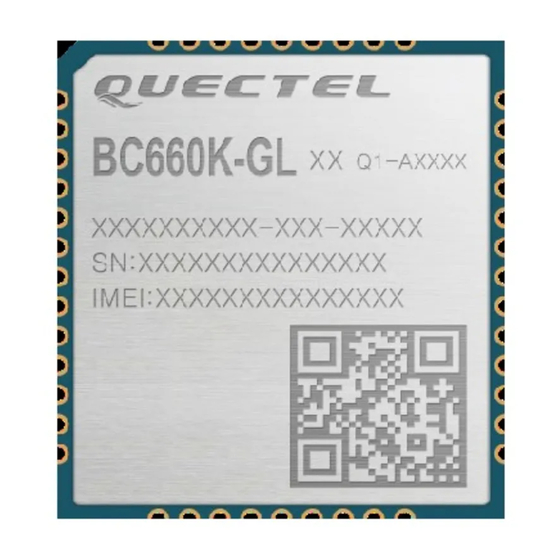
Figure 30: Top View of the Module Figure 31: Bottom View of the Module NOTE Images above are for illustration purpose only and may differ from the actual module. For authentic appearance and label, please refer to the module received from Quectel. BC660K-GL_Hardware_Design 50 / 57... -
Page 52: Storage, Manufacturing And Packaging
NB-IoT Module Series BC660K-GL Hardware Design Storage, Manufacturing and Packaging 7.1. Storage The module is provided with vacuum-sealed packaging. MSL of the module is rated as 3. The storage requirements are shown below. 1. Recommended Storage Condition: The temperature should be 23 ± 5 ° C and the relative humidity should be 35–60 %. -
Page 53: Manufacturing And Soldering
NB-IoT Module Series BC660K-GL Hardware Design NOTES This floor life is only applicable when the environment conforms to IPC/JEDEC J-STD-033. 2. To avoid blistering, layer separation and other soldering issues, it is forbidden to expose the modules to the air for a long time. If the temperature and moisture do not conform to IPC/JEDEC J-STD-033 or the relative moisture is over 60 %, it is recommended to start the solder reflow process within 24 hours after the package is removed. -
Page 54: Tape And Reel Packaging
NB-IoT Module Series BC660K-GL Hardware Design Table 28: Recommended Thermal Profile Parameters Factor Recommendation Soak Zone Max slope 1–3 ° C/s Soak time (between A and B: 150 ° C and 200 ° C) 70–120 s Reflow Zone Max slope 2–3 °... - Page 55 NB-IoT Module Series BC660K-GL Hardware Design Figure 33: Tape Dimensions (Unit: mm) Figure 34: Reel Dimensions (Unit: mm) BC660K-GL_Hardware_Design 54 / 57...
-
Page 56: Appendix References
BC660K-GL Hardware Design Appendix References Table 29: Related Documents Document Name Description Quectel_BC660K-GL-TE-B_User_Guide BC660K-GL-TE-B User Guide Quectel_BC660K-GL_AT_Commands_Manual BC660K-GL AT Commands Manual Quectel_BC660K-GL_Reference_Design BC660K-GL Reference Design Quectel_RF_Layout_Application_Note RF Layout Application Note Quectel_Module_Secondary_SMT_User_Guide Module Secondary SMT User Guide Table 30: Terms and Abbreviations... - Page 57 NB-IoT Module Series BC660K-GL Hardware Design HTTP Hyper Text Transfer Protocol HTTPS Hyper Text Transfer Protocol over Secure Socket Layer Input/Output kbps Kilo Bits Per Second Light Emitting Diode Long Term Evolution LwM2M Lightweight M2M MQTT Message Queuing Telemetry Transport...
- Page 58 NB-IoT Module Series BC660K-GL Hardware Design Transmitting Data UART Universal Asynchronous Receiver & Transmitter User Datagram Protocol User Equipment Unsolicited Result Code (U)SIM Universal Subscriber Identification Module VSWR Voltage Standing Wave Ratio Vmax Maximum Voltage Value Vnom Nominal Voltage Value...
Need help?
Do you have a question about the BC660K-GL and is the answer not in the manual?
Questions and answers