Table of Contents
Advertisement
Quick Links
Advertisement
Table of Contents

Subscribe to Our Youtube Channel
Related Manuals for Flex BMR474 ROA


Summary of Contents for Flex BMR474 ROA
- Page 1 Evaluation board BMR474 ROA 1286016 USER GUIDE...
- Page 2 The contents of this document are subject to revision without notice due to continued progress in methodology, design and manufacturing. Flex shall have no liability for any error or damage of any kind resulting from the use of this document.
-
Page 3: Table Of Contents
How to contact Flex ................4 Prerequisites ..................4 Reference Board ROA 128 6016 ............5 USB-PMBus adapter ................7 Connection of Flex KEP 910 17 USB-PMBus adapter ......7 Power-up and Power-down Instructions ..........7 Power-up instruction ................7 Power-down instruction ................8 Address and VSET Resistor .............. -
Page 4: Introduction
In order to operate the ROA 128 6016 board, the following is needed: • Power supply 6 – 15 V. • USB-PMBus adapter Flex KEP 910 17. It is only needed when the PMBus shall be used. The “Flex Power Designer” software package and a compatible Windows •... -
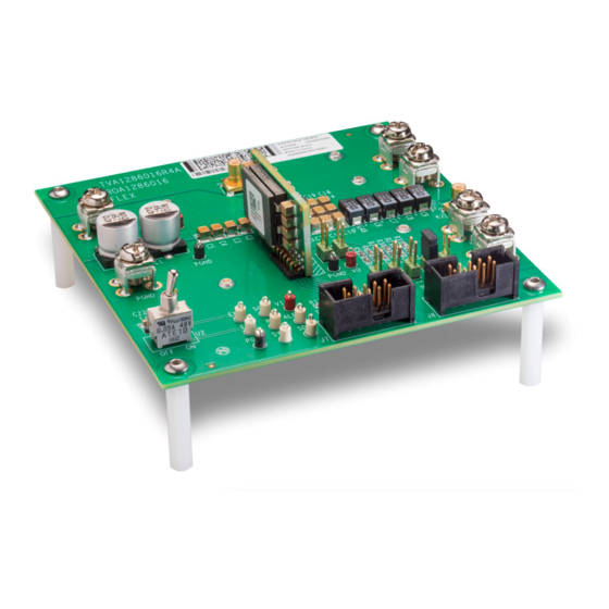
Page 5: Reference Board Roa 128 6016
Reference Board ROA 128 6016 In Figure 1a and 1b, the top and bottom sides of the ROA 128 6016 are shown. Figure 1a. ROA 128 6016 (top side) 28701-ROA1286016 Rev A 2021/4/25 5 (19) - Page 6 Output voltage probing points Position Description (Bottom Side) Output Polymer capacitors Diode for input anti-reverse protection Positions for populating Flex electronic load, ROA128 5552. Positions for additional input ceramic capacitors Positions for additional output ceramic capacitors 28701-ROA1286016 Rev A 2021/4/25...
-
Page 7: Usb-Pmbus Adapter
USB-PMBus adapter The USB-PMBus adapter used with this board is the Flex KEP 910 17. Connection of Flex KEP 910 17 USB-PMBus adapter Connect the Flex KEP 910 17 USB-PMBus adapter to the PMBus header, see position 5 in Figure 1a. -
Page 8: Power-Down Instruction
Make sure Enable switch is set to OFF position • • By default, the module is configured to set Vout with pin-strap resistors. Make sure jumper in the position 10 is populated with desired Vout. Connect power supply to connectors on position 1. •... -
Page 9: Adjustment Of Vset Resistors
R4 and R5 Figure 2 Address resistor position, R4 and R5, is shown in the picture. Adjustment of VSET resistors Populate a jumper in each “Vset” position to get the desired output voltage. The silk screen marking shows the voltage settings that can be achieved by populating jumpers. -
Page 10: Electronic Loads
additional input additional output capacitors capacitors Figure 3 Places for additional input/output capacitors. Electronic loads In order to perform load transient tests on the modules, up to 2 pcs of PuLS loads can be connected to the output of the board. The PuLS loads (ROA 128 5552) can be programmed for different transient loads and waveforms, see the technical specification for further information. -
Page 11: Bill Of Materials
Bill of Materials Designator Description CAP ALUM 470uF 20% 25V SMD C1, C47 C6,C7,C8,C9, 330uF 10% 6.3V polymer,CAPACITOR C43,C44,C45,C46,C48,C49 CAP TANT POLY 10uF 35V 2917 C23,C25 22uF 10% 1210 25V X7R,CAPACITOR C2,C3,C4,C5 C10,C11,C12,C13,C14,C15, 100uF 10% 1210 6.3V X7S,CAPACITOR C16,C17,C18,C19,C20,C21 100nF 10% 0805 25V X7R,CAPACITOR C22,C50 100nF 10% 0603 25V X7R,CAPACITOR C24,C26... -
Page 12: Layout Description
162kohm 1% 0603 0.1W,RESISTOR, -55C~155C 412kohm 1% 0603 0.1W,RESISTOR, -55C~155C 10kohm 1% 0603 0.1W,RESISTOR, -55C~155C R10,R11,R12 180ohm 1% 0603 0.1W,RESISTOR, -55C~155C R14,R15 100kohm 1% 0603 0.1W,RESISTOR, -55C~155C R17,R18 nfet_d3-g1-s2, BSS123, sot23 T1,T2 VS-43CTQ100SPBF,100V,2x20A, D2PAK(TO-263AB) Layout description The following sections describe how the layout guidelines provided in the ROA 128 6016. -
Page 13: Input Capacitance
Figure 4 Connection of power pins on top layer 11.2 Input capacitance The ceramic input capacitors should be placed as close as possible to the VIN/PGND pins to minimize the connection impedance. For the same reason, multiple vias are placed close to the capacitors’ terminals, utilizing inner layers to connect to input pins of the module. -
Page 14: Output Capacitance
11.3 Output capacitance Ceramic output capacitors are placed close to VOUT pins of the module to handle the module’s output ripple. Polymer capacitor are added to take care of load transient, see Technical Specification for load transient performance. It is important to secure low impedance connections Note there are places for additional output capacitors on the bottom side of the board, see section 7. - Page 15 Top side component layout Top layer 28701-ROA1286016 Rev A 2021/4/25 15 (19)
- Page 16 Layer 2 28701-ROA1286016 Rev A 2021/4/25 16 (19)
- Page 17 Layer 3 28701-ROA1286016 Rev A 2021/4/25 17 (19)
- Page 18 Bottom Layer 28701-ROA1286016 Rev A 2021/4/25 18 (19)
- Page 19 Bottom side component layout 28701-ROA1286016 Rev A 2021/4/25 19 (19)
Need help?
Do you have a question about the BMR474 ROA and is the answer not in the manual?
Questions and answers